Fraser Innovation FII-PRX100 User manual

V1.2
FRASER INNOVATION INC
FII-PRX100 Hardware Reference Guide

FII-PRX100 Hardware Reference Guide
Fraser Innovation Inc
1 / 53
Version Control
Version
Date
Description
1.0
07/11/2019
Initial Release
1.1
07/17/2019
Modification of HDMI and Segment Display Decoders
1.2
07/18/2019
Modification of JTAG Part

FII-PRX100 Hardware Reference Guide
Fraser Innovation Inc
2 / 53
Copyright Notice:
© 2019 Fraser Innovation Inc ALL RIGHTS RESERVED
Without written permission of Fraser Innovation Inc, no unit or individual may
extract or modify part of or all the contents of this manual. Offenders will be held
liable for their legal responsibility.
Thank you for purchasing the FPGA development board. Please read the manual
carefully before using the product and make sure that you know how to use the
product correctly. Improper operation may damage the development board. This
manual is constantly updated, and it is recommended that you download the
latest version when using.
Official Shopping Website:
https://fpgamarketing.com/FPGA-JTAG-ALTERAJTAG.htm

FII-PRX100 Hardware Reference Guide
Fraser Innovation Inc
3 / 53
Contents
1. Introduction........................................................................................................................................ 5
2. Basic Features ..................................................................................................................................10
1)FPGA.................................................................................................................................................10
2)Power Supply Interface ..............................................................................................................10
3)Segment Display Decoders....................................................................................................... 15
4)HDMI Interface..............................................................................................................................18
5)EEPROM AT24C02 .......................................................................................................................20
6)Gigabit Ethernet Interface.........................................................................................................21
7)Push Button.................................................................................................................................... 24
8)AD/DA Thermistor, Photoresistor and Potentiometer..................................................... 26
9)DIP Switch.......................................................................................................................................28
10)LED .................................................................................................................................................30
11)Configuration Chip FLASH......................................................................................................31
12)GPIO(PMOD)Expansion Interface ..................................................................................31
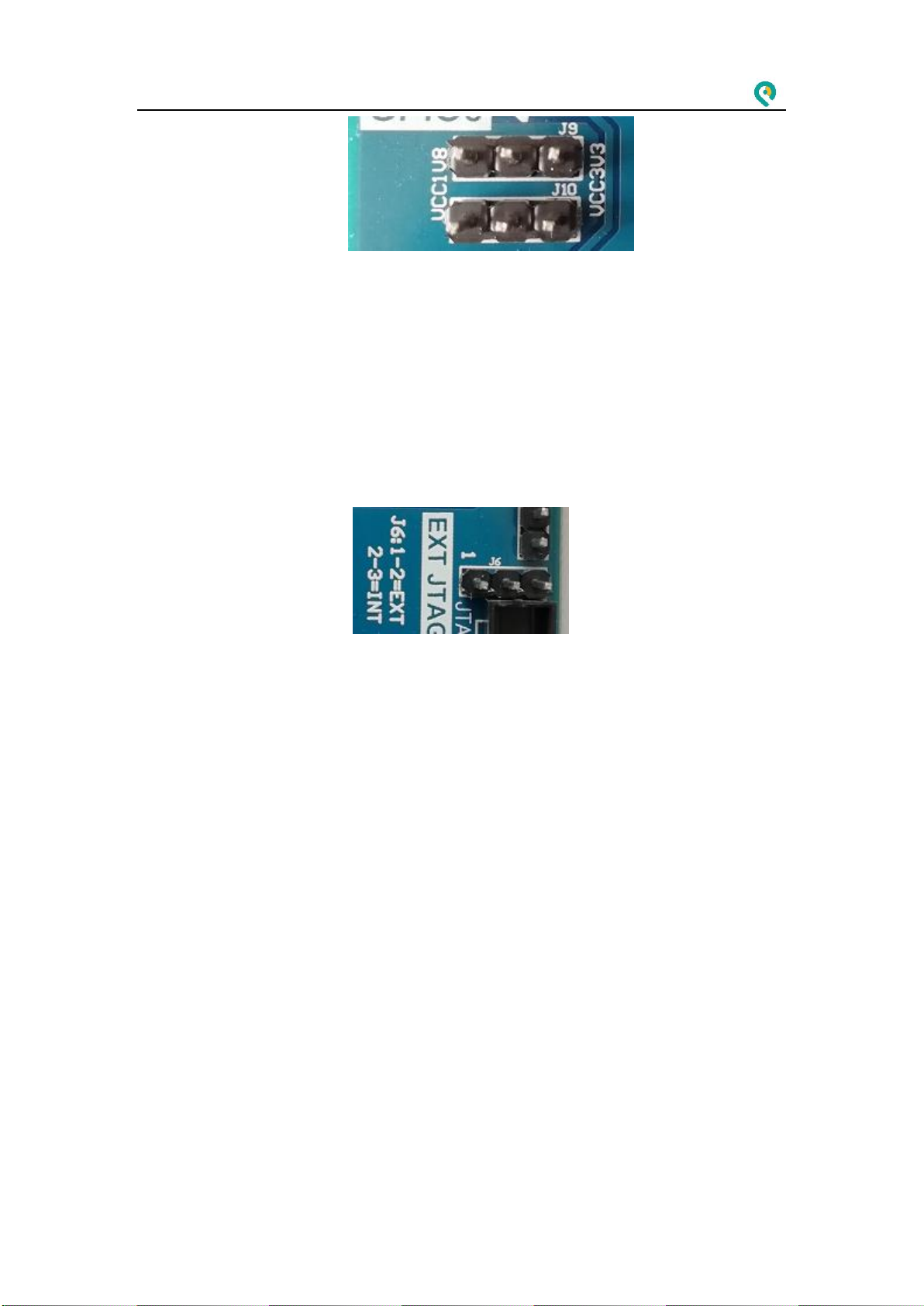
13)JTAG Interface.............................................................................................................................34
14)UART Interface............................................................................................................................ 36
15)SRAM .............................................................................................................................................38
16)Audio .............................................................................................................................................42
17)USB Keyboard and Mouse Interface ................................................................................... 43
18)TFT LCD Interface ......................................................................................................................46
19)40-pin Extended GPIO Interface ..........................................................................................48
20)High Speed Bus Connector....................................................................................................49
3. References ........................................................................................................................................53

FII-PRX100 Hardware Reference Guide
Fraser Innovation Inc
4 / 53
Fraser Innovation Inc develops FII-PRX100 based on the boards of the Xilinx
ARTIX-7 series. It was initial released in 2018. This development board is resource-
rich and high-speed, making it an ideal platform for learning and engineering
research. This development board has been spent a lot on system design, PCB
design, and function creation. It could even be said comprehensive and powerful.
PRX100 Development Board Full View

FII-PRX100 Hardware Reference Guide
Fraser Innovation Inc
5 / 53
1. Introduction
FII-PRX100 uses Xilinx's ARTIX-7 series chip, model XC7A100T-2FGG676I, which is
currently Xilinx's latest generation FPGA device.
The Artix-7 is one of the Xilinx 28nn FPGA families. It features a small form factor
package that reduces the power consumption of the Artix-7 family by half
compared to the Spartan-6 family.
PRX100 system block diagram:
Hardware resources:
•It can be powered by external 12V DC source or by “USB Power Supply
and Download Interface”. The latter also provides program download
functionality. Only one wire is to complete the power supply and download
functions;
FPGA
ARTIX-7
Gigabit
Ethernet
Interface
6 digits 7-
segment decoders
FLASH
128Mbit(Back)
Potentiometer
EEPROM
AT24C02(Back)
50M Oscillator
Power
Interface
AD/DA
(Back)
GPIO
Interface
External A/D Interface
8 LEDs
8 Switches
Reset
Figure 1 PRX100 System Block Diagram
Ethernet Chip
RTL8211E
USB1
USB2
USB3
USB4
7 Push Buttons
External I2C
Interface
USB Mouse
and
Keyboard
Control Chip
2 SRAMs
16Mbit
(Back)
GPIO Interface
GPIO Interface
Audio Input
Audio output
GPIO
Interface
PCIE
Interface
Photoresistor
Thermistor
Audio Chip
WM8978
40 bits GPIO
Interface
Power
Button
Voltage
Source
Selection
JTAG
HDMI
Video Chip
ADV7511
USB Power
Supply and
Download
Interface
USB-UART
Serial Chip
CP2102
External Serial Interface
TFTLCD Interface
32k
Oscillator

FII-PRX100 Hardware Reference Guide
Fraser Innovation Inc
6 / 53
•6-digit common anode 7-segment decoders, through dynamic scanning to
achieve data display;
•1 HDMI interface displaying color pictures or camera video;
•1 chip I2C interface EEPROM chip, model AT24C02;
•1 Gigabit Ethernet interface;
•8 push buttons, 7 for programmable buttons, 1 for reset button;
•1 photoresistor, through which it can simulate light control; 1 thermistor,
which can collect temperature or analog temperature alarm function; 1
potentiometer, which can simulate voltage change;
•1 PCF8591 AD/DA conversion chip, reserved external interface, free input
and output;
•Onboard 50MHz and 32.768kHz oscillators provide stable clock signals to
the development board;
•8-bit switch;
•8-bit LED;
•1 128Mbit Flash chip;
•4 GPIO external signal expansion interfaces, also the PMOD standard
interface;
•A 40-pin GPIO expansion interface that provides a large amount of I/O for
developers to use freely;

FII-PRX100 Hardware Reference Guide
Fraser Innovation Inc
7 / 53
•Two JTAG interfaces, one for the FPGA download debug interface (J4, J5)
and one for the RISC-V CPU JTAG debug interface(J16). Built-in RISC-V CPU
software debugger, no external RISC-V JTAG emulator required;
•1 UART asynchronous serial interface;
•2 SRAMs with a capacity of 16Mbit;
•a pair of audio input and output interfaces;
•1 PCIE interface;
•4 USB interfaces, 2 for the mouse and keyboard interface, 2 for the
universal serial interface;
•1 USB (USB-B) to UART interface for serial communication;
•1 TFTLCD touch screen interface, which can realize the display and
operation of the touch screen;

FII-PRX100 Hardware Reference Guide
Fraser Innovation Inc
8 / 53
Note: Before using development board, you need to check the following
1)Power supply jumper J23. If you are using an external power supply
interface, use a jumper cap to connect the two jumpers "EXT_5V" and
"PWR_5V". If you are using the "CPU_TAG" interface to supply power,
please connect "USB_5V" and "PWR_5V". As shown below:
Figure 1.2 External Power Supply Interface
Figure 1.3 USB Power Supply and Download Interface
Figure 1.4 Power Selection Jumper J23
2)Part of the FPGA BANK voltage is determined by selection jumpers J9, J10.
Voltage of BANK34 and BANK35 in development board, in order to adapt
to a variety of external signals, is adjustable power supply, specifically by
two common voltage options, 1.8V and 3.3V. Before the development
board works, please make sure that the jumpers of J9 and J10 are
connected. By default, you will be connected to 3.3V. As shown below:

FII-PRX100 Hardware Reference Guide
Fraser Innovation Inc
9 / 53
Figure 1.5 BANK Voltage Selection
3)The program download selection is jumper J6. Use the external
downloader to connect to the JTAG interface to download. J6 1-2
connection is downloaded when using the JTAG interface. As shown
below:
Figure 1.6 Program Download Selection Jumper J6

FII-PRX100 Hardware Reference Guide
Fraser Innovation Inc
10 / 53
2. Basic Features
The schematics quoted in this article are intended to highlight the key points, and the
circuits that are not related to the theme (such as protection circuits or filter circuits) will be
eliminated. Please pay attention to that. For the source material, please refer to the attached
schematic.
1)FPGA
As mentioned above, this development board FPGA model is XC7A100T-
2FGG676I, which is the latest generation of high-performance FPGA of Xilinx.
Figure 2.1 FPGA Physical Picture
Figure 2.2 Chip Resources
2)Power Supply Interface

FII-PRX100 Hardware Reference Guide
Fraser Innovation Inc
11 / 53
The development board has two power supply modes, one is for external 12V DC
power supply. (please use the power supply that comes with the development
board, do not use other specifications of the power supply to avoid damage to the
development board) Its power supply interface is as follows:
Figure 2.3 External Power Supply Interface
The second way is to use the USB cable to connect the "CPU_TAG" interface. See
Figure 2.4.
Figure 2.4 Internal Power Supply Interface
It should be noted that regardless of the power supply method, the power selection
jumper needs to be connected to the correct position. As shown below:
Figure 2.5 Power Supply Selection Jumpers
By the way to mention the power supply circuit of the development board
and the power supply of the FPGA. The external 12V power supply is converted to
a 5V power supply through the U19 power supply chip and connected to the pin 1

FII-PRX100 Hardware Reference Guide
Fraser Innovation Inc
12 / 53
of J23. The "PC_USB5V" power supply from the USB port is connected to the pin 3
of J23. With which of the two is connected to the 2nd pin, it powers the
development board. There is no problem when the two power supplies are
connected at the same time.
Figure 2.6 External Power Supply Schematics

FII-PRX100 Hardware Reference Guide
Fraser Innovation Inc
13 / 53
Figure 2.7 USB Power Supply Interface Schematics
We can see that after the PB8 is turned on, the power supply is connected to
the VCC5V0 level network of the development board, and then converted to the
1.0V (FPGA core voltage), 1.8V or 3.3V. Among them, 1.8V and 3.3V are the BANK
voltage of the FPGA. The two voltages are provided to meet the level standards of
various external signals. The conversion circuit is shown below.
Figure 2.8 Schematics of the 3.3V Power Supply

FII-PRX100 Hardware Reference Guide
Fraser Innovation Inc
14 / 53
Figure 2.9 Schematics of the 1.8V Power Supply
Figure 2.10 Schematics 1.0V Power Supply
If we look at the power supply of the FPGA, we can see these kinds of voltages (to
highlight the topic, the screenshot skips the irrelevant circuit):
Figure 2.11 Schematics of the FPGA Power Supply 1

FII-PRX100 Hardware Reference Guide
Fraser Innovation Inc
15 / 53
Figure 2.12 Schematics of the FPGA Power Supply 2
In Figure 2.11, 2.12, VCCO_0, VCCO_12, VCCO_13 and other pins are the BANK
power pins of the FPGA. VCCINT is the core power pin of the FPGA (the other
power supply parts of the FPGA are not listed. For more details, please refer to the
full version schematics).
3)Segment Display Decoders
Figure 3.1 Segment Decoders
One type of segment display is a semiconductor light-emitting device. The
segment display can be divided into a seven-segment display decoder and an
eight-segment display decoder. The difference is that the eight-segment display
decoder has one more unit for displaying the decimal point, the basic unit is a
light-emitting diode. The segment structure of the decoder is shown below:

FII-PRX100 Hardware Reference Guide
Fraser Innovation Inc
16 / 53
Figure 3.2 Segment Decoder Structure
Common anode decoders are used here. That is, the anodes of the LEDs are
connected.
Figure 3.3 Schematics of Common Anode Decoders
To illuminate a segment of an 8-segment decoder, the level of the
corresponding pin needs to be pulled low; when the pin is set high, the
corresponding field will not light. This development board uses a 6-in-one eight-
segment decoder. The schematics is shown below:

FII-PRX100 Hardware Reference Guide
Fraser Innovation Inc
17 / 53
Figure 3.4 Schematic of Decoders
The six-in-one decoder is a dynamic display. Due to the persistence of human
vision and the afterglow effect of the LED, although the decoders are not lit at the
same time, if the scanning speed is fast enough, the impression of human eyes is a
group of stable display data, no flickering can be noticed. The same segments of
the six-in-one decoders are connected, a total of eight pins, and with six control
signal pins, a total of 14 pins, as shown in Figure 3.4. Among them SEG_PA,
SEG_PB, SEG_PC, SEG_PD, SEG_PE, SEG_PF, SEG_PG, SEG_DP correspond to the A,
B, C, D, E, F, G, DP of decoder; SEG_3V3_D [0..5] are six control pins of the
decoders, which are also active low. When the control pin is low, the
corresponding decoder is powered, so that the LED can be lit.
Pin assignments of display decoders
Signal Name
FPGA Pin
Description
SEG PA
K26
Segment A
SEG PB
M20
Segment B
SEG PC
L20
Segment C

FII-PRX100 Hardware Reference Guide
Fraser Innovation Inc
18 / 53
SEG PD
N21
Segment D
SEG PE
N22
Segment E
SEG PF
P21
Segment F
SEG PG
P23
Segment G
SEG DP
P24
Segment DP
SEG_3V3_D0
R16
Decoder 1(from right)
SEG_3V3_D1
R17
Decoder 2(from right)
SEG_3V3_D2
N18
Decoder 3(from right)
SEG_3V3_D3
K25
Decoder 4(from right)
SEG_3V3_D4
R25
Decoder 5(from right)
SEG_3V3_D5
T24
Decoder 6(from right)
4)HDMI Interface
Image display processing has always been the focus of FPGA research. At
present, the image display mode is also constantly developing. The image display
interface is also gradually transitioning from the old VGA interface to the new DVI
or HDMI interface. HDMI is the abbreviation of High Definition Multimedia
Interface. It is a digital video/audio interface technology, which is a dedicated
digital interface for image transmission. It can transmit audio and video signals at
the same time.
The ADV7511 is a chip that converts VGA timing to HDMI timing. For details,
see the related chip manual. Among them, ADV7511_Programming_Guide and
ADV7511_Hardware_Users_Guide are the most important. You can configure the
registers of ADV7511 by viewing this document.

FII-PRX100 Hardware Reference Guide
Fraser Innovation Inc
19 / 53
Figure 4.1 HDMI Interface and ADV7511 Chip
HDMI pin assignment
Signal Name
FPGA Pin
HDMI- INT
E18
HDMI- SCL
R20
HDMI-SDA
R21
HDMI-VSYNC
A25
HDMI-HSYNC
C24
HDMI-CLK
B19
HDMI-HPD
H16
HDMI-D35
F15
HDMI-D34
E16
HDMI-D33
D16
HDMI-D32
G17
HDMI-D31
E17
HDMI-D30
F17
HDMI-D29
C17
HDMI-D28
A17
HDMI-D23
B17
HDMI-D22
C18
HDMI-D21
A18
HDMI-D20
D18
HDMI-D19
D20
HDMI-D18
A19
HDMI-D17
B20
HDMI-D16
A20
Table of contents
Popular Motherboard manuals by other brands

Silicon Laboratories
Silicon Laboratories Thunderboard EFR32BG22 user guide

ASROCK
ASROCK X570 Phantom Gaming-ITX/TB3 user manual

Yageo
Yageo KEMET USEQMSKS221600 user guide

Gigabyte
Gigabyte 8I845PE-RZ user manual

Infineon
Infineon OPTIREG PMIC TLF30682QVS01 user manual

Texas Instruments
Texas Instruments TLV62585PEVM-030 user guide