FUNAI 23C-250 User manual

SERVICE MANUAL
VIDEO CASSETTE RECORDER
Sec. 1: Main Section
●Specifications
●Preparation for Servicing
●Adjustment Procedures
●Schematic Diagrams
●CBA’ s
Sec. 2: Deck Mechanism Section
●Standard Maintenance
●Alignment for Mechanism
●Disassembly/Assembly of Mechanism
●Alignment Procedures of Mechanism
PAL
Sec. 3: Exploded views
and Parts List Section
●Exploded views
●Parts List
23C-250
23C-250A
H7700CVR

TABLE OF CONTENTS
Specifications..................................................................................................................................................... 1-1-1
Important Safety Precautions............................................................................................................................. 1-2-1
Standard Notes for Servicing............................................................................................................................. 1-3-1
Preparation for Servicing ................................................................................................................................... 1-4-1
Cabinet Disassembly Instructions...................................................................................................................... 1-5-1
Electrical Adjustment Instructions ...................................................................................................................... 1-6-1
Block Diagrams.................................................................................................................................................. 1-7-1
Function Indicator Symbols................................................................................................................................ 1-7-11
Schematic Diagrams / CBA’ s and Test Points .................................................................................................. 1-8-1
Waveforms......................................................................................................................................................... 1-9-1
Wiring Diagram .................................................................................................................................................. 1-10-1
IC Pin Function ...................................................................................................................................................1-11-1
Lead Identifications............................................................................................................................................ 1-12-1
MAIN SECTION
VIDEO CASSETTE RECORDER
23C-250 / 23C-250A
Sec. 1: Main Section
●Specifications
●Preparation for Servicing
●Adjustment Procedures
●Schematic Diagrams
●CBA’ s
H7700CVR

SPECIFICATIONS
Description Unit Minimum Nominal Maximum Remark
1. Video
1-1. Video Output (PB) Vp-p 0.8 1.0 1.2 FL6A
1-2. Video Output (R/P) Vp-p 0.8 1.0 1.2
1-3. Video S/N Y (R/P) dB 40 45 SP Mode,
W/O Burst
1-4. Video Color S/N AM (R/P) dB 37 41 SP Mode
1-5. Video Color S/N PM (R/P) dB 30 36 SP Mode
1-6. Resolution (PB) Line 230 245 SP Mode
2. Servo
2-1. Jitter Low µsec 0.07 0.12 SP Mode
2-2. Wow & Flutter % 0.3 0.5 SP Mode
3. Normal Audio
3-1. Output (PB) dBV -9 -6 -3 SP Mode
3-2. Output (R/P) dBV -9 -6 -1.5 SP Mode
3-3. S/N (R/P) dB 36 41 SP Mode
3-4. Distortion (R/P) % 1.0 4.0 SP Mode
3-5. Freq. resp (R/P) at 200Hz dB -11 -4 SP Mode
(-20dB ref. 1kHz) at 8kHz dB -14 -4 SP Mode
4. Tuner
4-1. Video output Vp-p 0.8 1.0 1.2 E-E Mode
4-2. Video S/N dB 39 42 E-E Mode
4-3. Audio output dB -10 -6 -2 E-E Mode
4-4. Audio S/N dB 40 46 E-E Mode
Note: Nominal specs represent the design specs. All units should be able to approximate these – some will exceed
and some may drop slightly below these specs. Limit specs represent the absolute worst condition that still might be
considered acceptable; In no case should a unit fail to meet limit specs.
1-1-1 H8740SP

IMPORTANT SAFETY PRECAUTIONS
Product Safety Notice
Some electrical and mechanical parts have special
safety-related characteristics which are often not evi-
dent from visual inspection, nor can the protection they
give necessarily be obtained by replacing them with
components rated for higher voltage, wattage, etc. Parts
that have special safety characteristics are identified by
a
!
on schematics and in parts lists. Use of a substi-
tute replacement that does not have the same safety
characteristics as the recommended replacement part
might create shock, fire, and/or other hazards. The
Product’s Safety is under review continuously and new
instructions are issued whenever appropriate. Prior to
shipment from the factory, our products are carefully
inspected to confirm with the recognized product safety
and electrical codes of the countries in which they are
to be sold. However, in order to maintain such compli-
ance, it is equally important to implement the following
precautions when a set is being serviced.
Precautions during Servicing
A.Parts identified by the
!
symbol are critical for
safety. Replace only with part number specified.
B.In addition to safety, other parts and assemblies are
specified for conformance with regulations applying
to spurious radiation. These must also be replaced
only with specified replacements.
Examples: RF converters, RF cables, noise block-
ing capacitors, and noise blocking filters, etc.
C.Use specified internal wiring. Note especially:
1) Wires covered with PVC tubing
2) Double insulated wires
3) High voltage leads
D.Use specified insulating materials for hazardous live
parts. Note especially:
1) Insulation tape
2) PVC tubing
3) Spacers
4) Insulators for transistors
E.When replacing AC primary side components
(transformers, power cord, etc.), wrap ends of wires
securely about the terminals before soldering.
F. Observe that the wires do not contact heat produc-
ing parts (heatsinks, oxide metal film resistors, fus-
ible resistors, etc.).
G.Check that replaced wires do not contact sharp
edges or pointed parts.
H.When a power cord has been replaced, check that
5 - 6 kg of force in any direction will not loosen it.
I.Also check areas surrounding repaired locations.
J.Use care that foreign objects (screws, solder drop-
lets, etc.) do not remain inside the set.
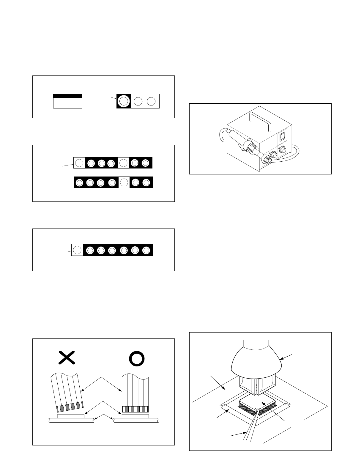
K.Crimp type wire connector
The power transformer uses crimp type connectors
which connect the power cord and the primary side
of the transformer. When replacing the transformer,
follow these steps carefully and precisely to prevent
shock hazards.
Replacement procedure
1)Remove the old connector by cutting the wires at a
point close to the connector.
Important: Do not re-use a connector. (Discard it.)
2)Strip about 15 mm of the insulation from the ends of
the wires. If the wires are stranded, twist the strands
to avoid frayed conductors.
3)Align the lengths of the wires to be connected. Insert
the wires fully into the connector.
4)Use a crimping tool to crimp the metal sleeve at its
center. Be sure to crimp fully to the complete closure
of the tool.
L.When connecting or disconnecting the internal con-
nectors, first, disconnect the AC plug from the AC
outlet.
1-2-1 H8740SFP

Safety Check after Servicing
Examine the area surrounding the repaired location for
damage or deterioration. Observe that screws, parts,
and wires have been returned to their original positions.
Afterwards, do the following tests and confirm the speci-
fied values to verify compliance with safety standards.
1. Clearance Distance
When replacing primary circuit components, confirm
specified clearance distance (d) and (d’) between sol-
dered terminals, and between terminals and surround-
ing metallic parts. (See Fig. 1)
Table 1 : Ratings for selected area
AC Line Voltage Clearance Distance (d) (d’)
230 V ≥3mm(d)
≥6 mm(d’)
Note: This table is unofficial and for reference only.
Be sure to confirm the precise values.
2. Leakage Current Test
Confirm the specified (or lower) leakage current be-
tween B (earth ground, power cord plug prongs) and
externally exposed accessible parts (RF terminals, an-
tenna terminals, video and audio input and output ter-
minals, microphone jacks, earphone jacks, etc.) is lower
than or equal to the specified value in the table below.
Measuring Method (Power ON) :
Insert load Z between B (earth ground, power cord plug
prongs) and exposed accessible parts. Use an AC
voltmeter to measure across the terminals of load Z.
See Fig. 2 and the following table.
AC Voltmeter
(High Impedance)
Exposed Accessible Part
BOne side of
Power Cord Plug Prongs
Z
Fig. 2
Table 2 : Leakage current ratings for selected areas
AC Line Voltage Load Z Leakage Current (i) One side of power cord plug
prongs (B) to:
230 V
2kΩRES.
Connected in
parallel
i≤0.7mA AC Peak
i≤2mA DC RF or
Antenna terminals
50kΩRES.
Connected in
parallel
i≤0.7mA AC Peak
i≤2mA DC A/V Input, Output
Note: This table is unofficial and for reference only. Be sure to confirm the precise values.
Chassis or Secondary Conductor
dd'
Primary Circuit Terminals
Fig. 1
1-2-2 H8740SFP

STANDARD NOTES FOR SERVICING
Circuit Board Indications
a.The output pin of the 3 pin Regulator ICs is indicated
as shown.
b.For other ICs, pin 1 and every fifth pin are indicated
as shown.
c.The 1st pin of every male connector is indicated as
shown.
Instructions for Connectors
1.When you connect or disconnect the FFC (Flexible
Foil Connector) cable, be sure to first disconnect the
AC cord.
2.FFC (Flexible Foil Connector) cable should be in-
serted parallel into the connector, not at an angle.
How to Remove / Install Flat Pack-IC
1. Removal
With Hot-Air Flat Pack-IC Desoldering Machine:
(1)Prepare the hot-air flat pack-IC desoldering ma-
chine, then apply hot air to the Flat Pack-IC (about
5 to 6 seconds). (Fig. S-1-1)
(2)Remove the flat pack-IC with tweezers while apply-
ing the hot air.
(3)Bottom of the flat pack-IC is fixed with glue to the
CBA; when removing entire flat pack-IC, first apply
soldering iron to center of the flat pack-IC and heat
up. Then remove (glue will be melted). (Fig. S-1-6)
(4)Release the flat pack-IC from the CBA using tweez-
ers. (Fig. S-1-6)
Caution:
1.Do not supply hot air to the chip parts around the flat
pack-IC for over 6 seconds because damage to the
chip parts may occur. Put masking tape around the
flat pack-IC to protect other parts from damage.
(Fig. S-1-2)
2.The flat pack-IC on the CBA is affixed with glue, so
be careful not to break or damage the foil of each
pin or the solder lands under the IC when removing
it.
Hot-air
Flat Pack-IC
Desoldering
Machine
CBA
Flat Pack-IC
Tweezers
Masking
Tape
Top View
Out In
Bottom View
Input
5
10
Pin 1
Pin 1
FFC Cable
Connector
CBA
* Be careful to avoid a short circuit.
Fig. S-1-2
Fig. S-1-1
1-3-1 NOTE_1

With Soldering Iron:
(1)Using desoldering braid, remove the solder from all
pins of the flat pack-IC. When you use solder flux
which is applied to all pins of the flat pack-IC, you
can remove it easily. (Fig. S-1-3)
(2)Lift each lead of the flat pack-IC upward one by one,
using a sharp pin or wire to which solder will not
adhere (iron wire). When heating the pins, use a fine
tip soldering iron or a hot air desoldering machine.
(Fig. S-1-4)
(3)Bottom of the flat pack-IC is fixed with glue to the
CBA; when removing entire flat pack-IC, first apply
soldering iron to center of the flat pack-IC and heat
up. Then remove (glue will be melted). (Fig. S-1-6)
(4)Release the flat pack-IC from the CBA using tweez-
ers. (Fig. S-1-6)
With Iron Wire:
(1)Using desoldering braid, remove the solder from all
pins of the flat pack-IC. When you use solder flux
which is applied to all pins of the flat pack-IC, you
can remove it easily. (Fig. S-1-3)
(2)Affix the wire to a workbench or solid mounting point,
as shown in Fig. S-1-5.
(3)While heating the pins using a fine tip soldering iron
or hot air blower, pull up the wire as the solder melts
so as to lift the IC leads from the CBA contact pads
as shown in Fig. S-1-5.
(4)Bottom of the flat pack-IC is fixed with glue to the
CBA; when removing entire flat pack-IC, first apply
soldering iron to center of the flat pack-IC and heat
up. Then remove (glue will be melted). (Fig. S-1-6)
(5)Release the flat pack-IC from the CBA using tweez-
ers. (Fig. S-1-6)
Note:
When using a soldering iron, care must be taken to
ensure that the flat pack-IC is not being held by glue.
When the flat pack-IC is removed from the CBA,
handle it gently because it may be damaged if force
is applied.
Flat Pack-IC Desoldering Braid
Soldering Iron
Fig. S-1-3
Fine Tip
Soldering Iron
Sharp
Pin
To Solid
Mounting Point
Soldering Iron
Iron Wire
or
Hot Air Blower
Fig. S-1-4
Fig. S-1-5
Fine Tip
Soldeing Iron
CBA
Flat Pack-IC
Tweezers
Fig. S-1-6
1-3-2 NOTE_1

2. Installation
(1)Using desoldering braid, remove the solder from the
foil of each pin of the flat pack-IC on the CBA so you
can install a replacement flat pack-IC more easily.
(2)The " ●" mark on the flat pack-IC indicates pin 1.
(See Fig. S-1-7.) Be sure this mark matches the 1
on the PCB when positioning for installation. Then
pre- solder the four corners of the flat pack-IC. (See
Fig. S-1-8.)
(3)Solder all pins of the flat pack-IC. Be sure that none
of the pins have solder bridges.
Instructions for Handling
Semiconductors
Electrostatic breakdown of the semiconductors may
occur due to a potential difference caused by electro-
static charge during unpacking or repair work.
1. Ground for Human Body
Be sure to wear a grounding band (1MΩ) that is properly
grounded to remove any static electricity that may be
charged on the body.
2. Ground for Workbench
Be sure to place a conductive sheet or copper plate with
proper grounding (1MΩ) on the workbench or other
surface, where the semiconductors are to be placed.
Because the static electricity charge on clothing will not
escape through the body grounding band, be careful to
avoid contacting semiconductors with your clothing.
CBA
CBA
Grounding Band
Conductive Sheet or
Copper Plate
1MΩ
1MΩ
Presolder
CBA
Flat Pack-IC
Example :
Pin 1 of the Flat Pack-IC
is indicated by a " ●" mark.
Fig. S-1-7
Fig. S-1-8
< Incorrect >
< Correct >
1-3-3 NOTE_1

PREPARATION FOR SERVICING
How to Enter the Service Mode
About Optical Sensors
Caution:
An optical sensor system is used for the Tape Start and
End Sensors on this equipment. Carefully read and
follow the instructions below. Otherwise the unit may
operate erratically.
What to do for preparation
Insert a tape into the Deck Mechanism Assembly and
press the PLAY button. The tape will be loaded into the
Deck Mechanism Assembly. Make sure the power is
on, connect TP502 (SENSOR INHIBITION) to GND.
This will stop the function of Tape Start Sensor, Tape
End Sensor and Reel Sensors. (If these TPs are con-
nected before plugging in the unit, the function of the
sensors will stay valid.) See Fig. 1.
Note: Because the Tape End Sensors are inactive, do
not run a tape all the way to the start or the end of the
tape to avoid tape damage.
About REC-Safety Switch
Caution:
The REC-Safety Switch is directly mounted on the Main
CBA. When the Deck Mechanism Assembly is removed
from the Main CBA for servicing, this switch does not
work automatically.
What to do for preparation
In order to record, press the Rec button while pushing
REC-SAFETY SW on the Main CBA. See Fig. 1.
CN251
CN501
CN504 CN506
CN503
TP502
S-INH
(REC-SAFETY SW)
SW506
Q503
Q504
Fig. 1
1-4-1 H8740PFS

CABINET DISASSEMBLY INSTRUCTIONS
1. Disassembly Flowchart
This flowchart indicates the disassembly steps to gain
access to item(s) to be serviced. When reassembling,
follow the steps in reverse order. Bend, route, and dress
the cables as they were originally.
Disassembly Method
ID/
LOC.
No. PART
REMOVAL
Fig.
No.
REMOVE/
*UNHOOK/UNLOCK/
RELEASE/UNPLUG/
DESOLDER
Note
[1] Top Case 1 6(S-1) -
[2] Front
Assembly 2 *3(L-1), *4(L-2) -
[3] Jack CBA 3 3(S-2), (CN101) -
[4] Function
CBA 2, 4 *(L-3), (CN505) 1
[5]
Deck
Assembly 5,7 6(S-3), Spacer
*(CN251, CN501,
CN503, CN504,
CN506)
2, 4
[6] Cylinder
Shield 52(S-4) -
[7] REC Arm
Assembly 5 ---------- -
[8] Main CBA 6 3(S-5), *2(L-4) 3
↓
➀↓
➁↓
➂↓
➃↓
➄
Reference Notes
CAUTION: Locking Tabs (L-1) and (L-2) are fragile. Be
careful not to break them.
1. Disconnect Connector (CN505) to remove Function
CBA. Hold Main CBA while pulling up on the Func-
tion CBA. (Fig. 4)
2. Remove six Screws (S-3) and the Spacer. Then
slowly lift the Deck Assembly up. Lifting Deck As-
sembly disconnects five Connectors (CN251,
CN501, CN503, CN504, CN506) . (Fig. 5)
3. When reassembling the unit, always reinsert Lock-
ing Tabs (L-4), and then reinstall Screws (S-5).
These screws are critical for proper shielding of the
Main CBA. (Fig. 7)
4. Before installing the Deck Assembly, be sure to
place the pin of LD-SW on Main CBA as shown in
Fig. 7. Then, install the Deck Assembly while align-
ing the hole of Cam Gear with the pin of LD-SW, the
shaft of Cam Gear with the hole of LD-SW as shown
in Fig. 7.
[2] Front Assembly
[1] Top Case
[3] Jack CBA
[4] Function CBA [5] Deck Assembly
[6] Cylinder Shield
[7] REC Arm Assembly
[8] Main CBA
1 : Identification (location) No. of parts in the figures
2 : Name of the part
3 : Figure Number for reference
4 : Identification of parts to be removed, unhooked, un-
locked, released, unplugged, unclamped, or
desoldered.
P=Spring, L=Locking Tab, S=Screw,
CN=Connector
*=Unhook, Unlock, Release, Unplug, or Desolder
e.g. 2(S-2) = two Screws (S-2),
2(L-2) = two Locking Tabs (L-2)
5 :Refer to "Reference Notes."
1-5-1 H8740DC

(S-3)
[5]Deck Assembly
[6]Cylinder
Shield
[7]REC Arm
Assembly
(S-3) (S-4)
CN501
CN504
CN251 CN506
CN503
Spacer
Fig. 5
(L-2)
(L-1) [2]Front Assembly
(L-2)
[4]Function C.B.A.
Fig. 2
(L-3)
Lift PCB up and
over tab
[4] Function CBA
CN505
[8] Main CBA
Fig. 4
[3] Jack CBA
(S-2)
(S-2)
(S-2)
CN101
Fig. 3
(S-1)
(S-1)
[1]Top Case
(S-1)
Fig. 1
1-5-2 H8740DC

[8]Main C.B.A.
SW507
LD-SW
LD-SW Pin
Hole
Hole
Shaft
Cam Gear
[8]Main C.B.A.
[5]Deck Assembly
Triangle Marks
Fig. 7
(S-5)
(L-4)
(L-4)
[8]Main C.B.A.
Fig. 6
1-5-3 H8740DC

ELECTRICAL ADJUSTMENT INSTRUCTIONS
General Note: "CBA" is an abbreviation for "Circuit
Board Assembly".
Notes:
1.Electrical adjustments are required after replacing
circuit components and certain mechanical parts. It
is important to do these adjustments only after all
repairs and replacements have been completed.
Also, do not attempt these adjustments unless the
proper equipment is available.
2.To perform these alignment / confirmation proce-
dures, make sure that the tracking control is set in
the center position: Press either channel "▼" or "▲"
button first, then the " PLAY " button (VCR’s Front
Panel only).
Test Equipment Required
1.Oscilloscope: Dual-trace with 10:1 probe, V-Range:
0.001~50V/Div., F-Frange: AC~DC-20MHz
2.Alignment Tape ( FL6A )
1. Head Switching Position
Adjustment
Purpose: To determine the Head Switching point dur-
ing playback.
Symptom of Misadjustment: May cause Head
Switching noise or vertical jitter in the picture.
Test Point Adj. Point Mode Input
TP751(V-OUT)
TP502(RF-SW)
GND VR501 (SW-P) PLAY
(SP) ----
Tape Measurement
Equipment Spec.
FL6A Oscilloscope 6.5H±1H
(412.7±60µs)
Connections of Measurement Equipment
Figure 1
Reference Note:
TP502, TP751, VR501 : Main CBA
•Play back the test tape and adjust VR501 so that the
V-sync front edge of the CH1 video output wave-
form is at the 6.5H(412.7µs) delayed position from
the rising edge of the CH2 head switching pulse
waveform.
EXT. Synchronize Trigger Point
V-Sync
0.5H1.0H
6.5H
Switching Pulse
CH2
CH1
GND
Main CBA
TP502
TP751
CH1 CH2
Oscilloscope
Trig. (+)
1-6-1 H8740EA

M
M
CN506
DRUM
MOTOR
PG
SENSOR
1LD-M(-)
2LD-M(+)
LOADING
MOTOR
CONTROL
HEAD
CN287
5 8CTL(+)
6 9CTL(-)
CN504
CN504
1C-F/R
2P-ON+5V
3
AL+15V/+12V
4C-FG
5C-POW-SW
6C-DRIVE
7
FG-GND
8CM-GND
CN503
CAPSTAN
MOTOR
CYLINDER ASSEMBLY
LOADING MOTOR ASSEMBLY
AC HEAD ASSEMBLY
MAIN CBA
CAPSTAN MOTOR
KEY-2
RF-SW
C-FG
D-FG
D-PG
PB-CTL
ST-S
T-REEL
C-CONT
C-F/R
KEY-1
V-ENV
REMOCON
REC-CTL(+)
RESET
C-ROTA
D-REC-H D-REC-H
PG-DELAY
A-MUTE-H
I2C BUS SCL-2
I2C BUS SDA-2
A-MUTE-H
RF-SW
V-ENV
I2C BUS SCL-1
I2C BUS SDA-1
C-ROTA
END-S
IC501
(SERVO/SYSTEM CONTROL)
1
53
52
54
19
REC-CTL(-)
20
51
75
68
49
34
66
55
71
17
15
70
9
10
62
60
5
73
72
RS501
REMOTE
SENSOR
LM-
FWD/REV
59
D-CONT56
AL+5V
P-ON+5V
D555
S-LED
(MEMORY)
IC505
(DRUM /LOADING MOTOR DRIVE)
IC506
IC503
Servo/System Control Block Diagram BLOCK DIAGRAMS
END-S
END-S
T-REEL
ST-S
Q503 Q504
Q501
RESET
SW508
RESET
Q506 S-REEL
50
C-POW-SW46
SW-POINT
AL+5VVR501
TIMER+5V
TP506
S-REEL
PS502
DEC-L DEC-L
79
SECAM-H 23
TRICK-H 47
SECAM-CHARA-H 2
SECAM-H
TRICK-H
SECAM-CHARA-H
I2C BUS SCL-1
I2C BUS SDA-1
I2C BUS SCL-1
I2C BUS SDA-1
TO VIDEO
BLOCK
TO AUDIO
BLOCK
I2C BUS SDA-1
I2C BUS SCL-1 TO JACK
BLOCK
2 2KEY-2
KEY
SWITCH KEY SWITCH
TP501
GND
TP507
S-INH
CN651CN505
FUNCTION CBA
1-7-1 1-7-2 H8743BLS
SCL
SDA
TU701
SCL
SDA
6
5
25
24
22
21
16
15
10
9814
17
4
2
18
14
20
LD-SW74
DRUM
MOTOR
DRIVE
DRIVE LOADING
MOTOR
CONTROL
+
-
+
-
13
12
+
-
P-ON+5V
AL+15V/+12V
SCL
SDA
4
AL+5V
SW507
LD-SW
(1/3)
TP501 CTL
G1
G4
a
e
f
g
88
85
97
93
98
92
j89
FP502
F I P
TIMER LED
CASETTE-IN LED 92
91
REC LED 87
D595 STAND-BY
D598 CAS
D597 TIMER
D596 REC
D599 P-ON
P-ON+5V
AL+5V
11
5
12
3
(DECK ASSEMBLY)
9
M
REC-SAF-SW 25
SW506
REC-SAFETY
AL+5V
Q620~Q623
DRIVE
G1
G6
a
f
g
83
88
93
98
92
j89
FP501
F I P
G1
G6
P1
P6
P7
83
88
93
98
92
P10 89
FIP501
F I P
Comparison Chart of
Models & Marks
Model Mark
VR421CAT
VR621CAT
A
B
VR421CAT
VR621CAT
A
B
1D-W
2D-V
3D-U
4D-COM
5PG-IN

VIDEO (L) HEAD
CYLINDER ASSEMBLY
VIDEO (R) HEAD
V(L)
V-COM
V(R)
CN251
1
2
3
10
Video Block Diagram
1-7-3 1-7-4 H8743BLV
(DECK ASSEMBLY)
BUFFER
Q305
BUFFER
Q308
C-SYNC C-SYNC
OSD-BB-OUT
C-ROTA
TU701
CN751
TO CN101
FROM/TO
JACK BLOCK
TP751 V-OUT
TU-VIDEO 24
26
FBC
VXO
CHARA
INS.
Y/C
MIX
PIC-CTL
ANR
KILL
B.D.
AMP
NOISE
CANCEL
M
DE EMPA
CCD 1H
DELAY
1/2 Y-LPF
CLAMP
L
R
REC FM
AGC
PB FM
AGC
FM
DEMOD.
DOUBLE
LIMIT
V/I
CONV
SUB
LPF
SERIAL
DECORDER
11
93 V-ENV
RF-SW
TO
SERVO/SYSTEM
CONTROL BLOCK
C-ROTA
ENV DET TP502 RF-SW
TO
SERVO/SYSTEM
CONTROL BLOCK
I2C BUS SDA-1
I2C BUS SCL-1
C-LPF
R P
R
P
R P
R P
R/P
B/B R
PDOC YNR Y/C COMB
ACC B-UP
AMP
MAIN
CONV
R
R
P
P
R P
SUB
CONV
4.43MHz
629KHz
21 24 2320
IC301
IC501
(Y/C PROCESS) 29 67 66 49
X302
4.43MHz
43 45 46 41
Q307
REC-VIDEO SIGNAL PB-VIDEO SIGNAL MODE: SP/REC
BUFFER
Q304
Q371
Q372
BUFFER
88
89
90
91
72715759 54 52 51 61
28
D-V SYNCD-V SYNC
25
27
21
31
30
33
OSD-CHARA-OUT
38
17
19
18
MAPBPF
BPF
D.E.
NL
EMPHA
C-COMB COMB
AMP
CCD
LPF
BPF
KIL
Q302,
Q303 PEAKING
AMP
V-OUT 7
V-IN 5
TU-VIDEO 19
32 31 EE
AGC
CLAMP
REC
FM-EQ
PB
FM-EQ
FM
MOD
DETAIL
ENH
W/D
CLIP
CLAMP
MAIN CBA
74
WF2
WF1 IC370 (PAL/SECAM DECTECOTR)
VXO/XO/OUT2 5
VIDEO-SW
3
C-PB
PAL/SECAM
DETECTOR
9
5
3
9
TRICK-H 8
REC-C OUT
10
C-SYNC 1
8
10
1
SECAM-H 77
SECAM CBA
CN370CN371
2
15
13
1
17
27
26
26
TRICK-H
TO SERVO/SYSTEM
CONTROL BLOCK
SECAM-H
TP301 C-PB WF5
BUFFER
Q311
AMP
Q310
Q309
SECAM-CHARA-H BUFFER
BUFFER

Audio Block Diagram
98
REC
AMP
7
6
AUTO
BIAS
99
P-ON+5V
P-ON+5V
Q401
BIAS
OSC
Q402
Q404 (PB=ON)
Q405
(PB=ON)
Q403
SWITCHING
D-REC-OFF
4EQ
AMP
100
1
2
LINE
AMP MUTE 96
3
PB-ON
SP/LP-ON
P
R
ALC
IC301
(AUDIO PROCESS) 76
TU701
TU-AUDIO 21
J981
A-OUT
7 A-PB/REC
CN504
6 A-COM
4 AE-H
5 FE-H
A-PB/REC 4
A-COM 3
AE-H 1
AE-H/FE-H 2
CN287
AUDIO
HEAD
AUDIO
ERASE
HEAD
ACE HEAD ASSEMBLY
FE HEAD
1 FE-H
2 FE-H-GND
CN501
1-7-5 1-7-6 H8743BLA
MAIN CBA
PB-AUDIO SIGNAL REC-AUDIO SIGNAL Mode : SP/REC
1030
D-REC-H
A-MUTE-H
I2C BUS SCL-1
I2C BUS SDA-1
TO SERVO/SYSTEM
CONTROL BLOCK
FULL
ERASE
HEAD
23 24
SERIAL
DECODER
CN751
TO CN101
TO
JACK BLOCK
TU-AUDIO 13
A-OUT 3
A-IN 1
(DECK ASSEMBLY)

2
4
16
6
7
Power Supply Block Diagram
CAUTION
FOR CONTINUED PROTECTION AGAINST FIRE HAZARD,
REPLACE ONLY WITH THE SAME TYPE T1.6AL/250V FUSE.
NOTE :
The voltage for parts in hot circuit is measured using
hot GND as a common terminal.
CAUTION !
Fixed voltage (or Auto voltage selectable ) power supply circuit is used in this unit.
If Main Fuse (F001) is blown, check to see that all components in the power supply
circuit are not defective before you connect the AC plug to the AC power supply.
Otherwise it may cause some components in the power supply circuit to fail.
H8743BLP1-7-7 1-7-8
COLD
MAIN CBA
HOT CIRCUIT. BE CAREFUL.
HOT
IC001
ERROR
VOLTAGE DET
Q002
Q003
Q001
F001
T1.6AL/250V L003
LINE
FILTER
BRIDGE
RECTIFIER
D001 - D004
1
2
3
4
Q004
(SHUNT REGULATOR)
REG
AC001
T001
P-ON+44V
12
P-ON-H
AL+15V/+12V
AL+9V
AL+12V
DEC/PB-L
D-PB+12V
C-POW-SW
AL+5V
TIMER+5V
P-ON+5V
P-DOWN-L
Q051
Q055
Q054
Q056
Q052
Q057
Q058
13
15
14
11
17
18

Jack Block Diagram
CN101TO CN751
TO VIDEO BLOCK
V-IN 5
V-OUT 7
TU-VIDEO 19
CN101TO CN751
TO SERVO/SYSTEM
CONTROL BLOCK
DEC-L 11
I2C BUS SCL-1 17
I2C BUS SDA-1 18
CN101TO CN751
TO AUDIO BLOCK
A-IN 1
TU-AUDIO 13
A-OUT 3
19
20
CLAMP CLAMP
CLAMP
CLAMP
BUF
BUF
BUF
BUF AMP
AMP
6dB
6dBDRIVE
A
B
SW1
A
SW2
B
C
A
SW3
B
C
JK101
V-OUT
V-IN
V-OUT
V-IN
DEC-L
A-OUT
A-IN
A-OUT
A-IN
A-OUT
A-IN
A-OUT
A-IN
1
2
3
6
JK101
1
2
3
6
JK102
19
20
JK102
8
JK102
IC101
INPUT/OUTPUT SELECT
(1/2)
21
20
19
23
25
14
16
18
AL+5V
Q101
26
29
31
35
36
9
5
1
A
B
SW1-L
A
SW2-L
B
C
A
SW3-L
B
C
SERIAL
CONTROL
IC101(2/2)
INPUT/OUTPUT SELECT
1-7-9 1-7-10 H8743BLJ
PB-AUDIO SIGNAL REC-VIDEO SIGNAL
REC-AUDIO SIGNAL PB-VIDEO SIGNAL
DRIVE
JACK CBA

FUNCTION INDICATOR SYMBOL
Note:
The following symbols will appear on the indicator panel to indicate the current mode or operation of the VCR.
On-Screen modes will also be momentarily displayed on the TV screen when you press the operation buttons.
Display panel
LED MODE INDICATOR ACTIVE
CASSETTE "IN"
CASSETTE "OUT" " "
" " ON
OFF
CLOCK " 88:88 " ON
COUNTER " -8:88:88 " ON
ON
OFF
POWER ON " PWR. " ON
REC " REC " ON
REC PAUSE " REC " Blinks at 0.8Hz interval
T-REC, OTR " " ON
(T-REC OFF, T-REC incomplete
Blinks at 0.8Hz interval)
When reel and capstan mechanism is not
functioning correctly " "
" No.1 " Blinks at 0.8Hz interval
When tape loading mechanism is not
functioning correctly " "
" No.2 " Blinks at 0.8Hz interval
When cassette loading mechanism is not
functioning correctly " "
" No.3 " Blinks at 0.8Hz interval
When the drum is not working properly " "
" No.4 " Blinks at 0.8Hz interval
VPS/PDC "ON"
"OFF"
P-ON Power safety detection " "
" No.5 " Blinks at 0.8Hz interval
" "
" "
" "
PWR.
AM
PM
VCR
1-7-11 H8743FIS

SCHEMATIC DIAGRAMS / CBA’S AND TEST POINTS
Standard Notes
WARNING
Many electrical and mechanical parts in this chassis
have special characteristics. These characteristics
often pass unnoticed and the protection afforded by
them cannot necessarily be obtained by using replace-
ment components rated for higher voltage, wattage, etc.
Replacement parts that have these special safety char-
acteristics are identified in this manual and its supple-
ments; electrical components having such features are
identified by the mark "
!
" in the schematic diagram
and the parts list. Before replacing any of these compo-
nents, read the parts list in this manual carefully. The
use of substitute replacement parts that do not have the
same safety characteristics as specified in the parts list
may create shock, fire, or other hazards.
Capacitor Temperature Markings
Mark Capacity
change rate Standard
temperature Temperature
range
(B) ±10% 20°C -25~+85°C
(F) +30 -80% 20°C -25~+85°C
(SR) ±15% 20°C -25~+85°C
(Z) +30 -80% 20°C -10~+70°C
Note:
1.Do not use the part number shown on these draw-
ings for ordering. The correct part number is shown
in the parts list, and may be slightly different or
amended since these drawings were prepared.
2.All resistance values are indicated in ohms (K=103,
M=106).
3.Resistor wattages are 1/4W or 1/6W unless other-
wise specified.
4.All capacitance values are indicated in µF
(P=10−6µF).
5.All voltages are DC voltages unless otherwise speci-
fied.
6.Electrical parts such as capacitors, connectors, di-
odes, IC’s, transistors, resistors, switches, and
fuses are identified by four digits. The first two digits
are not shown for each component. In each block
of the diagram, there is a note such as shown below
to indicate these abbreviated two digits.
(Top View) (Bottom View)
(Bottom View)
Electrolytic Capacitor
+
Transistor or Digital Transistor
NPN Transistor PNP Transistor
NPN Digital Transistor PNP Digital Transistor
(Top View)
(Top View)
E C B
E C B
Digital Transistor
CBA Symbols Schematic Diagram Symbols
E C B
(Top View)
(Top View)
E C B
E C B
-
Capacitors and transistors are represented by the following symbols.
1-8-1 SCPA1
This manual suits for next models
1
Table of contents
Other FUNAI VCR System manuals

FUNAI
FUNAI PV910 User manual

FUNAI
FUNAI F220LB User manual

FUNAI
FUNAI F260LA User manual

FUNAI
FUNAI 29A-650 User manual

FUNAI
FUNAI Symphonic SL240B User manual

FUNAI
FUNAI SC-690 User manual

FUNAI
FUNAI PV910A User manual

FUNAI
FUNAI 29C-854 User manual

FUNAI
FUNAI 31B-254 User manual

FUNAI
FUNAI 29D-850 User manual