GS66508B-EVBDB1
650V GaN E-HEMT Evaluation Board User’s Guide
___________________________________________________________________________________________________________________
GS66508B-EVBDB1 UG rev. 190605 © 2019 GaN Systems Inc. www.gansystems.com 2
Please refer to the Evaluation Board/Kit Important Notice on page 30
Overview
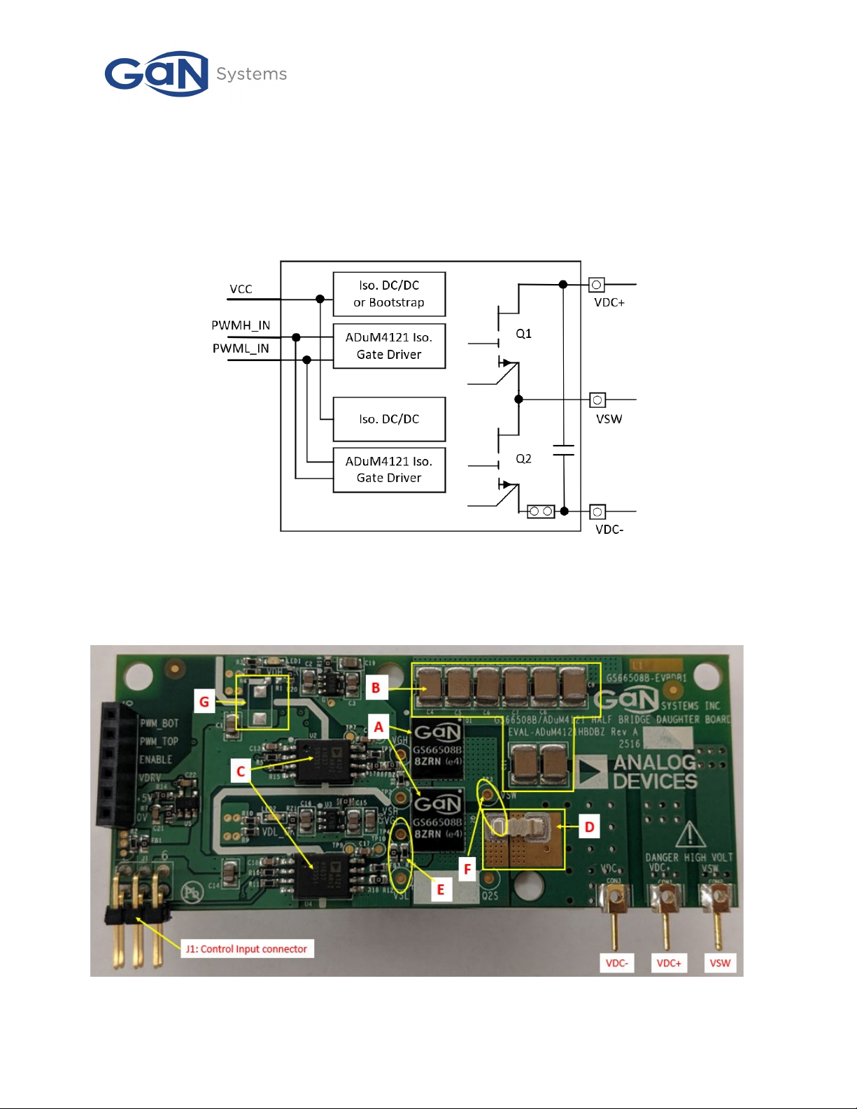
The GS66508B-EVBDB1 daughter board style evaluation kit consists of two GaN Systems 650V GaN
Enhancement-mode HEMTs (E-HEMTs) and all necessary circuits including half bridge gate drivers,
isolated power supplies and optional heatsink to form a functional half bridge power stage. It allows
users to easily evaluate the GaN E-HEMT performance in any half bridge-based topology, either with the
universal mother board (P/N: GS665MB-EVB) or for quick prototyping of a users’ own system design.
Features
•Serves as a reference design and evaluation tool as well as deployment-ready solution for easy in-
system evaluation.
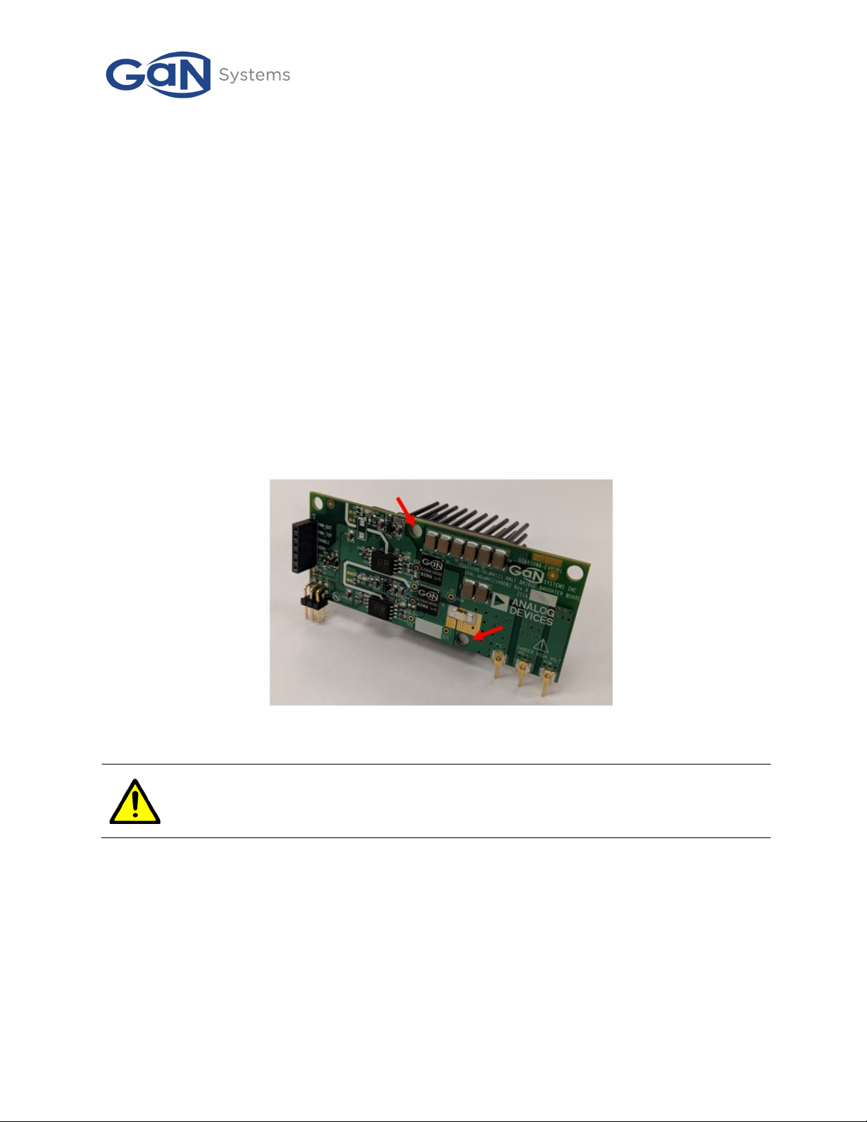
•Vertical mount style with height of 35mm, which fits in majority of 1U design and allows
evaluation of GaN E-HEMT in traditional through-hole type power supply board.
•Current shunt position for switching characterization testing
•Universal form factor and footprint for all products
The daughter board and universal mother board ordering part numbers are below:
Table 1 Ordering part numbers
Part Number GaN E-HEMT
Description
GS66508B-EVBDB1 GS66508B GaN E-HEMT bottom side cooled 650V/30A, 50mΩ
Analog Devices isolated driver ADUM4121ARZ
Universal 650V Mother Board
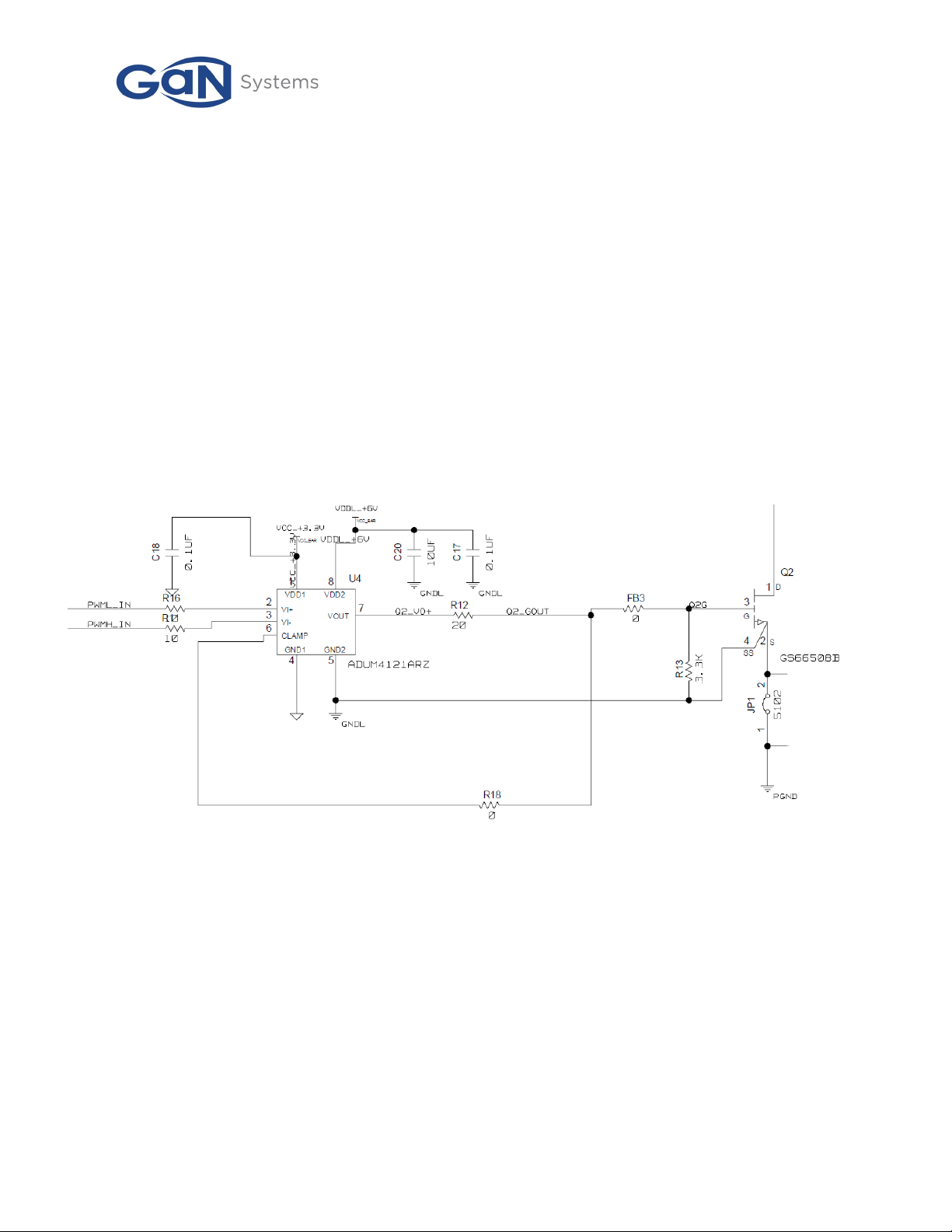
Control and Power I/Os
The daughter board GS6650B8-EVBDB1 circuit diagram is shown in Figure 1. The control logic inputs on
2x3 pin header J1 are listed below:
Table 2 Control pins
Enable input. It is internally pulled up to VCC, a low logic disables all the PWM gate
drive outputs.
VCC +5V auxillary power supply input for logic circuit and gate driver. On the daughter
board there are 2 isolated 5V to 9V DC/DC power supplies for top and bottom switches.
Optional 9V gate drive power input. This pin allows users to supply separate gate drive
power supply. By default VDRV is connected to VCC on the daughter board via a 0 ohm
jumper FB1. If bootstrap mode is used for high side gate drive, connect VDRV to 9V
High side PWM logic input for top switch Q1. It is compatible wth 3.3V and 5V
Low side PWM logic input for bottom switch Q2. It is compatible wth 3.3V and 5V
Logic inputs and gate drive power supply ground return.