GS65011-EVBEZ
EZDrive®Open Loop Boost Evaluation Board
Technical Manual
_____________________________________________________________________________________________________________________
GSWPT-EVBEZ Rev. 210307 © 2021 GaN Systems Inc. www.gansystems.com 7
Please refer to the Evaluation Board/Kit Important Notice on page 17
Circuit Description
The GS65011-EVBEZ EVB is a GaN-based open-loop DC/DC Boost converter. It is
assembled with the EZDrive®GaN driving circuit, a Si MOSFET PWM controller
(TL1454ACNSR) and a 650V 5×6 mm PDFN package GaN E-HEMT, (GS-065-011-1-L).
The PWM control signal is generated internally by the PWM controller, U2.
The EZDrive®uses a Si MOSFET controller to drive a GaN HEMT which has a lower
threshold voltage than a Si MOSFET. The EZDrive®circuit is shown in the dotted box in
Figure 2. It is a low-cost, low component-count circuit composed of two Zener diodes,
one capacitor, three resistors and one diode.
ZDEZ1, ZDEZ2 clamp the positive and negative gate drive voltages. CEZ holds a negative
voltage for GaN E-HEMT turn-off. REZ sets the minimum driving current required to
keep the GaN E-HEMT fully turned on. RGcontrols the turn-on speed and ROFF controls
the turn-off speed.
The two operation modes for EZDrive®are:
•Mode 1: Assuming the Vcc of the controller is 12V and the controller output is
ON, the driving voltage on the GaN E-HEMT is clamped to 6V by Zener diode
ZDEZ. The rest of the Vcc, 6V, is stored across the capacitor CEZ.
•Mode 2: The voltage stored in CEZ is applied to the gate in reverse, allowing the
GaN E-HEMT e to be turned off quickly.
This circuit converts the Si MOSFET PWM controller’s output voltage to the proper
voltage thresholds for driving GaN Systems’ E-HEMTs.
Cautionary Notes
A Boost converter’s output voltage is higher than the input voltage, VIN.When operating
at a high duty cycle and low load/no load operating conditions, the output voltage will
rise and has the potential of damaging the GaN device. To avoid an overvoltage on the
GaN device, two actions are recommended.
First, always apply a load at the output voltage, VOUT.
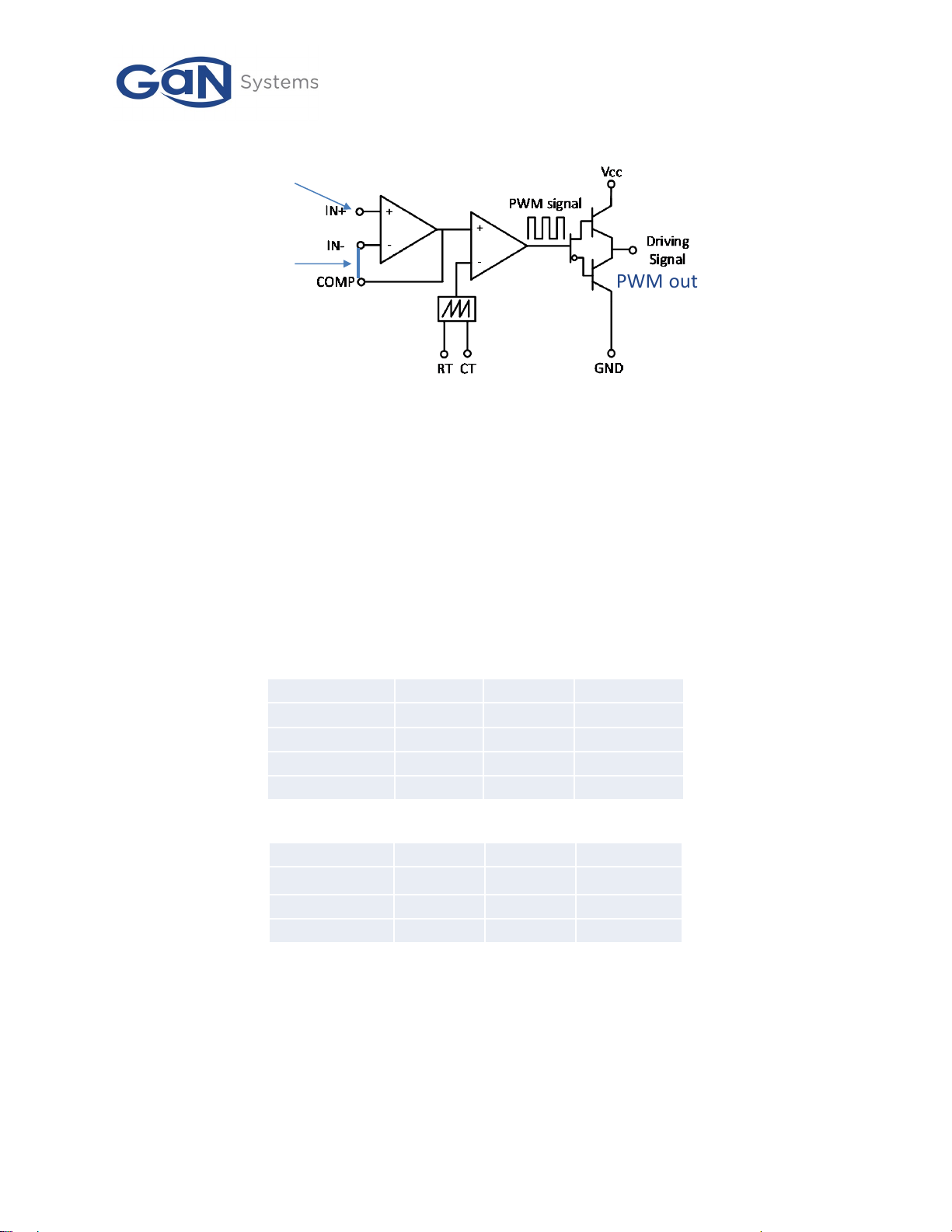
Secondly, pre-set the PWM signal before applying power to VIN. Figure 4 shows the block
diagram of PWM signal generation inside the TL1454ACNSR.