Gemalto Cinterion PLS62-W User manual

GEMALTO.COM/M2M
Getting Started with Cinterion®PLS62-W
User Guide
Version: 01
DocId: PLS62-W_startup_guide_v01

GENERAL NOTE
THE USE OF THE PRODUCT INCLUDING THE SOFTWARE AND DOCUMENTATION (THE "PROD-
UCT") IS SUBJECT TO THE RELEASE NOTE PROVIDED TOGETHER WITH PRODUCT. IN ANY
EVENT THE PROVISIONS OF THE RELEASE NOTE SHALL PREVAIL. THIS DOCUMENT CONTAINS
INFORMATION ON GEMALTO M2M PRODUCTS. THE SPECIFICATIONS IN THIS DOCUMENT ARE
SUBJECT TO CHANGE AT GEMALTO M2M'S DISCRETION. GEMALTO M2M GMBH GRANTS A NON-
EXCLUSIVE RIGHT TO USE THE PRODUCT. THE RECIPIENT SHALL NOT TRANSFER, COPY,
MODIFY, TRANSLATE, REVERSE ENGINEER, CREATE DERIVATIVE WORKS; DISASSEMBLE OR
DECOMPILE THE PRODUCT OR OTHERWISE USE THE PRODUCT EXCEPT AS SPECIFICALLY
AUTHORIZED. THE PRODUCT AND THIS DOCUMENT ARE PROVIDED ON AN "AS IS" BASIS ONLY
AND MAY CONTAIN DEFICIENCIES OR INADEQUACIES. TO THE MAXIMUM EXTENT PERMITTED
BY APPLICABLE LAW, GEMALTO M2M GMBH DISCLAIMS ALL WARRANTIES AND LIABILITIES.
THE RECIPIENT UNDERTAKES FOR AN UNLIMITED PERIOD OF TIME TO OBSERVE SECRECY
REGARDING ANY INFORMATION AND DATA PROVIDED TO HIM IN THE CONTEXT OF THE DELIV-
ERY OF THE PRODUCT. THIS GENERAL NOTE SHALL BE GOVERNED AND CONSTRUED
ACCORDING TO GERMAN LAW.
Copyright
Transmittal, reproduction, dissemination and/or editing of this document as well as utilization of its con-
tents and communication thereof to others without express authorization are prohibited. Offenders will be
held liable for payment of damages. All rights created by patent grant or registration of a utility model or
design patent are reserved.
Copyright © 2018, Gemalto M2M GmbH, a Gemalto Company
Trademark Notice
Gemalto, the Gemalto logo, are trademarks and service marks of Gemalto and are registered in certain
countries. Microsoft and Windows are either registered trademarks or trademarks of Microsoft Corpora-
tion in the United States and/or other countries. All other registered trademarks or trademarks mentioned
in this document are property of their respective owners.
PLS62-W_startup_guide_v01 2018-05-17
Confidential / Released
Getting Started with Cinterion®PLS62-W
2
Page 2 of 17
User Guide: Getting Started with Cinterion®PLS62-W
Version: 01
Date: 2018-05-17
DocId: PLS62-W_startup_guide_v01
Status: Confidential / Released

Getting Started with Cinterion®PLS62-W
Contents
17
PLS62-W_startup_guide_v01 2018-05-17
Confidential / Released
Page 3 of 17
Contents
0 Document History ...................................................................................................... 4
1 Introduction ................................................................................................................. 5
1.1 Supported Products ........................................................................................... 5
1.2 Related Documents ........................................................................................... 6
2 Getting Started with PLS62-W ................................................................................... 7
2.1 Technical Requirements for Using PLS62-W Modules...................................... 7
2.2 Connecting the PLS62-W Evaluation Module to the DSB75 ............................. 8
2.3 Start Up the Module ......................................................................................... 11
3 Appendix: DSB75 Adapter ....................................................................................... 13
4 Appendix: Circuit Diagrams for Evaluation Module Board................................... 15

Getting Started with Cinterion®PLS62-W
1 Introduction
12
PLS62-W_startup_guide_v01 2018-05-17
Confidential / Released
Page 5 of 17
1 Introduction
This document describes a ready-to-use development and test environment for the Cinterion®
PLS62-W SMT modules.
The development and test environment comprises the following hardware components
• PLS62-W evaluation module (for supported products see Section 1.1)
The PLS62-W evaluation module consists of the actual PLS62-W SMT module soldered
onto a PCB with a board-to-board connector and an U.FL antenna connector. For PLS62-
W evaluation module board schematics see Chapter 4.
• DSB75 Development Support Board
The PLS62-W evaluation module needs to connect to an adequate host device such as the
DSB75. A detailed DSB75 hardware interface description and operating instructions can be
found in [3].
• DSB75 Adapter.
The DSB75 Adapter is used to mount the PLS62-W evaluation module to the DSB75.
The purpose of this document1is to guide you through the process of connecting the hardware,
installing the supplied drivers on a Microsoft®Windows 7 (or Windows 8) system and getting
started with PLS62-W.
Note: The hardware components listed above as part of a development and test environment
are also mentioned in [2] as part of the comprehensive reference equipment used by Gemalto
M2M for type approval. For general development and test purposes however, there is alterna-
tive equipment available: The DSB75 may be replaced by the DSB-Mini (for details see [5]),
the DSB75 Adapter by the Starter Kit B80, either plugged onto the DSB-Mini or as a stand-
alone device (for more information see [6]).
1.1 Supported Products
This document applies to the following Gemalto M2M modules:
•Cinterion
®PLS62-W
1. The document is effective only if listed in the appropriate Release Notes as part of the technical docu-
mentation delivered with your Gemalto M2M wireless module.

Getting Started with Cinterion®PLS62-W
1.2 Related Documents
12
PLS62-W_startup_guide_v01 2018-05-17
Confidential / Released
Page 6 of 17
1.2 Related Documents
[1] PLS62-W AT Command Set
[2] PLS62-W Hardware Interface Description
[3] DSB75 Development Support Board Hardware Interface Description
[4] Java User‘s Guide
[5] DSB-Mini User Guide
[6] Starter Kit B80 User Guide

Getting Started with Cinterion®PLS62-W
2 Getting Started with PLS62-W
12
PLS62-W_startup_guide_v01 2018-05-17
Confidential / Released
Page 7 of 17
2 Getting Started with PLS62-W
2.1 Technical Requirements for Using PLS62-W Modules
• PLS62-W evaluation module2. For PLS62-W evaluation module schematics see Appendix:
Circuit Diagrams for Evaluation Module Board.
• PLS62-W USB driver package
• Computer running Windows 7 (or Windows 8), USB 2.0 High Speed compatible
• Local administrator privileges on the particular Windows computer to install and uninstall
the drivers
• DSB75 Development Support Board (for details see [3])
• DSB75 Adapter required for mounting the evaluation module to the DSB75. For more infor-
mation about the DSB75 Adapter please refer to Appendix: DSB75 Adapter.
• Accessories:
- Small 50 Ohms antenna adapter cables with SMT connectors to connect the U-FL con-
nectors on the PLS62-W evaluation module to the U.FL connectors on DSB75 Adapter
(e.g. a Hirose - Hirose cable such as delivered with each DSB75) - 1 for GSM/UMTS/LTE
main antenna connection, 1 for UMTS/LTE Rx Diversity antenna connection.
- External 50 Ohms RF antenna with SMA connector to connect the SMA connector on the
DSB75 Adapter (e.g. a SMARTEQ MiniMag antenna such as delivered with each
DSB75) - 1 for GSM/UMTS/LTE main antenna connection, 1 for UMTS/LTE Rx Diversity
antenna connection.
- 9 to 15 Volts power supply adapter applied at the DSB75 for powering up the DSB75 and
the connected PLS62-W evaluation module (not supplied by Gemalto M2M)
- RS-232 cables for the module's asynchronous serial interfaces ASC0 and ASC1 (not
supplied by Gemalto M2M)
- USB cable with mini-USB plug (not supplied by Gemalto M2M)
• Appropriate application for controlling the module from within a PC’s operating system. For
Windows, e.g. Windows Hyperterminal.
2. For ordering information see [2].

Getting Started with Cinterion®PLS62-W
2.2 Connecting the PLS62-W Evaluation Module to the DSB75
12
PLS62-W_startup_guide_v01 2018-05-17
Confidential / Released
Page 8 of 17
2.2 Connecting the PLS62-W Evaluation Module to the DSB75
To properly connect the PLS62-W evaluation module and all accessories to the DSB75 please
complete the steps listed below. The complete setup with the evaluation module mounted onto
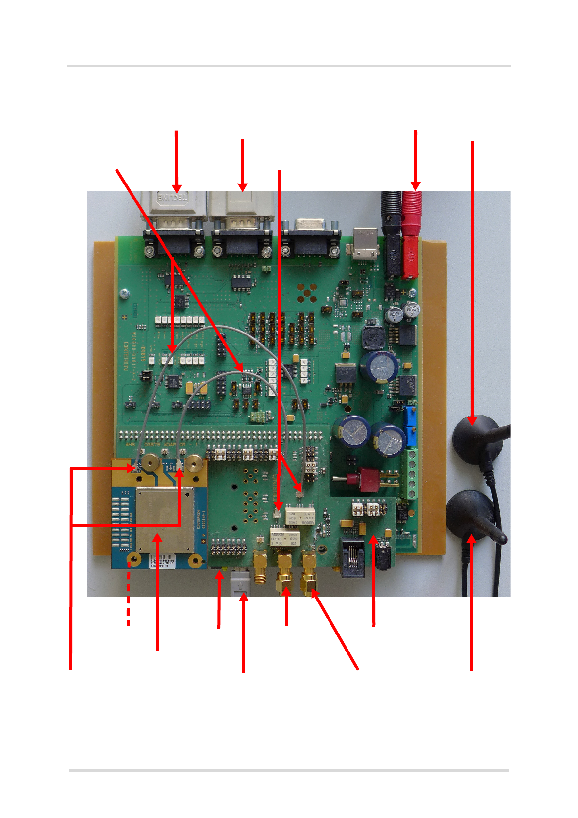
the DSB75 Adapter and the DSB75 Adapter connected to the DSB75 is shown in Figure 2.
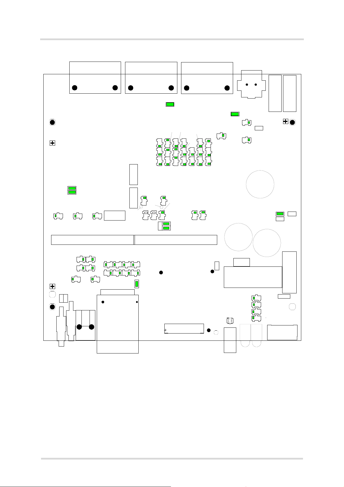
• Ensure that all jumpers and slide switches on the DSB75 are set to their default positions
as shown in Figure 1 and in [3].
• Attach the 80-pin header of the DSB75 Adapter to the 2x40-pin connector (X101/X202)
located on the DSB75. Take gentle care that all pins are aligned correctly, then press down
evenly on the adapter until it is firmly seated.
• Remove the knurled nuts from the DSB75 Adapter.
• Mount the PLS62-W evaluation module onto the 80-pin board-to-board connector X120 of
the DSB75 Adapter.
• Fasten the knurled nuts to secure the module to the DSB75 Adapter.
• Use the small antenna cables to connect the U.FL GSM/UMTS/LTE main antenna connec-
tor and the U.FL UMTS/LTE Rx Diversity antenna connector on the PLS62-W evaluation
module to the U.FL-R SMT connectors on the DSB75 Adapter:
- for GSM/UMTS/LTE main antenna connect to X350
- for UMTS/LTE Rx Diversity antenna connect to X352
• Screw the external antennas to the appropriate SMA connectors on the DSB75 Adapter:
- GSM/UMTS/LTE main antenna to X353
- UMTS/LTE Rx Diversity antenna connect to X351
• Insert the SIM card into the card reader located at the DSB75 Adapter.
Note: Do not use the SIM card reader of the DSB75 Support Board.
• To employ the module’s USB interface, plug the USB 2.0 Mini-B5 connector of the USB
cable to the Mini-B5 USB jack at the DSB75 Adapter. The other end of the USB cable con-
nects to a Windows PC.
Note: Do not use the USB connector located on the DSB75 Support Board.
• To employ the module’s asynchronous serial interfaces ASC0 and/or ASC1, connect the 9-
pin SubD connectors on the DSB75 to the PC’s UART COM ports using the RS-232 cables.
Use COM1 (X201) for the first serial interface ASC0 and/or COM2 (X202) for second serial
interface ASC1.
• Make sure that the power supply adapter delivers a minimum of 12 Volts, and connect the
power cables to the red (X400 = BATT+) and black (X401 = Ground) connectors of the
DSB75 Support Board.
After connecting the PLS62-W evaluation module to the DSB75, the module can be switched
on. The initial startup and possible USB driver installation are described in Section 2.3.

Getting Started with Cinterion®PLS62-W
2.2 Connecting the PLS62-W Evaluation Module to the DSB75
12
PLS62-W_startup_guide_v01 2018-05-17
Confidential / Released
Page 9 of 17
Figure 1: DSB75 configuration
X202 X201 X205
X400X401
X110
X120
S112
S110
X121
S111
C413
X410
X411
X405
C415
C414
X510
X511
X551X552
X122
S601
X602
X710 TP105
X700
S714
S715
S710
S711
V430V431
X505
X506
TP106
X100
X503X502
X501
X500
S307
S305S303S301
S300 S302 S 304 S306
S713 S712
S717 S716
S730
S731
S420
TP104
X420 X421
X101 X102
S201 S200
X554
X703
X561
X560
X562
S504
S503
S502
TP501
TP502
S501S500
S457S452
S456
S455
S453
S454
S450
S460
S451
S461
S462
S464
S465
S463
S466
S469
S459
S467
S458 S468
1
2
31
2
31
2
3
1
10
1
2
3
1
2
3
1
2
3
12
3
1
2
3
1
2
3
39
40
1
2
1
2
31
2
3
1
2
31
2
3
1
2
31
2
3
3
2
13
2
13
2
13
2
1
3
2
13
2
13
2
13
2
1
1
2
3
4
8
456 7
12 3
18
1
11
1
2
3
13
13
13
1
12
1
1
5
1
1
2
3
1
1
1
2
3
1
2
3
1
2
3
1
2
3
1
2
3
1
2
3
1
2
3
1
2
3
1
2
3
1
2
3
1
2
3
1
2
3
1
2
3
1
2
3
1
2
3
1
2
3
1
2
3
1
2
3
1
2
3
1
2
3
1
2
3
1
2
3
1
2
3
1
1
11
1
11
1 4 2 3
15
69
15
69
15
69
39
40
1
2
1
1
1
2
2
910
910
2
9
123
456
X203
1
X206
X204
1
1
X600
1
DSB75
S421
(X701 bottom side)

Getting Started with Cinterion®PLS62-W
2.2 Connecting the PLS62-W Evaluation Module to the DSB75
12
PLS62-W_startup_guide_v01 2018-05-17
Confidential / Released
Page 10 of 17
Figure 2: Module mounted onto DSB75 Adapter and connected to DSB75
PLS62-W
IGT switch
SMA connector (X353)
DSB75
USB cable at mini USB
RS-232 cable at
COM2 (X202) for
ASC1
Power supply
(X400/X401)
50 Ohms
U.FL -R SMT connector (X350/X391)
GSM/UMTS/LTE
Antenna cables
linking U.FL
antenna connectors
connector on DSB75 Adapter
SMA connector
GSM/UMTS/LTE
for GSM/UMTS/LTE main antenna
UMTS/LTE Rx
50 Ohms
RS-232 cable at
COM1 (X201) for
ASC0
UMTS/LTE Rx
U.FL connectors
LTE Rx
and UMTS/LTE Rx Diversity antenna
main antenna
Diversity antenna
Diversity antenna
Diversity
Main
Antenna
Antenna
(X351)
Main antenna
SIM Card
Holder
Evaluation module
Adapter

Getting Started with Cinterion®PLS62-W
2.3 Start Up the Module
12
PLS62-W_startup_guide_v01 2018-05-17
Confidential / Released
Page 11 of 17
2.3 Start Up the Module
After connecting the PLS62-W evaluation module to the DSB75 as described in Section 2.2,
the module can be switched on.
Note: If the USB interface is to be employed, the USB drivers provided by Gemalto M2M need
to be available. Copy the supplied driver files to a folder on the Windows computer. Be sure to
use the latest USB driver software supplied by Gemalto M2M.
Also, if the module‘s Java functionality is to be employed, the Cinterion Mobility Toolkit (CMTK)
as distributed on the Java CD install package needs to be installed. For more information on
the CMTK (including installation) please refer to [4].
• Start the Windows PC.
• Press the ignition switch S421 on the DSB75. The ignition switch
is located on the component side of the DSB75 as shown in Fig-
ure 2.
• If the USB cable was plugged as described above, and the USB
drivers provided by Gemalto M2M were not yet installed on the
computer, you will be prompted to install them:
- On Windows 7 (or Windows 8), wait a few seconds until all
USB devices show up in the Windows Device Manager under
“Other devices” as devices without installed drivers. Then -
from top to bottom - right-click each “ELSx” device, select the option "Update Driver Soft-
ware...", browse to the folder you copied the Gemalto USB drivers to, and select this
folder to update the driver software from.
- In any case, cancel any Windows instructions to update the software automatically. For
each USB device take care to browse to the folder containing the unzipped driver soft-
ware.
After successful USB driver installation the installed USB devices are listed in the Windows
Device Manager under "Modems", “Network adapters”, and "Ports (COM & LPT)" as shown
in Figure 3.
Figure 3: Installed USB devices
IGT switch

Getting Started with Cinterion®PLS62-W
2.3 Start Up the Module
12
PLS62-W_startup_guide_v01 2018-05-17
Confidential / Released
Page 12 of 17
• To connect to the PLS62-W evaluation module via USB interface, check the properties of
the enumerated USB devices for the configured COM ports, for example the "Cinterion
PLSx USB Modem", call a terminal program on the PC and connect to the configured COM
port. Type the AT command ATI to display module identification information.
Figure 4: Connection via USB interface (USB modem)
• To connect to the PLS62-W evaluation module via asynchronous serial interface, for exam-
ple ASC0, check for the port that is connected to the DSB75’s COM1 X201 via RS-232
cable, call a terminal program on the PC and connect to the PLS62-W evaluation module
using the following initial settings:
- Bits per seconds: 115200
- Data bits: 8
- Parity: None
- Stop bits:1
- Flow control: Hardware
Type the AT command ATI to display module identification information.
Figure 5: Connection via ASC0 interface
For a complete AT Command Set description see [1]. This includes AT commands to con-
figure the communication interfaces.

Getting Started with Cinterion®PLS62-W
3 Appendix: DSB75 Adapter
16
PLS62-W_startup_guide_v01 2018-05-17
Confidential / Released
Page 13 of 17
3 Appendix: DSB75 Adapter
The PLS62-W Evaluation Module connects to the 80-pin board-to-board connector X120 on
top of the DSB75 Adapter. The 2x40-pin header X101/X102 of the DSB75 Support Board con-
nects to the 80-pin female connector X135 located on the back of the DSB75 Adapter.
By default, when shipped from factory, all jumpers on the DSB75 Adapter are set for use with
PLS62-W, even though not all of them are required - see Figure 7.
The adapter is illustrated in Figure 6 and Figure 7.
Figure 6: DSB75 Adapter with default jumper positions
X135 (test points on top
and connector on bottom)
X308/X309
X305
X311
Handset jack X310
TTY jack X307
SMA antenna connectors
X390, X351, X353
USB 2.0 Mini-B5 connector X306
SIM interface X171
SIM card reader X170
80-pin board-to-board connector X120
X350
X352
X391

Getting Started with Cinterion®PLS62-W
3 Appendix: DSB75 Adapter
16
PLS62-W_startup_guide_v01 2018-05-17
Confidential / Released
Page 14 of 17
Figure 7: DSB75 Adapter - connectors, jumpers
X311
Relais
Relais
X391
X390 X 351 X353
X171
2
1
14
13
X310 X307
2
1
X352
1
41
40
2
X350
1
2
79
80
X135
MICN1D
MICP1D
MICN1
EPN1
EPP1
MICP1D
EPP1
MICN1D_I
MICP1D_I
MICP1
EPN1_I
EPP1_I
MICP1 _TTY
EPP1_TTY
CCIO
CCRST
GND
GND
CCV CC
CCCLK
CCIN
DCD0
ON
BATT+ 1 2 GND
BATT+ 5 6 GND
BATT+ 3 4 GND
BATT+ 7 8 GND
BATT+ 9 10 GND
11 12
RING0 13 14
DSR0 15 16 VDDLP
RTS0 17 18 TXD0
DTR0 19 20 TXD1
RTS1 21 22 RXD0
CTS0 23 24 RXD1
CTS1 25 26 STATUS_LED
DCD0 27 28
EMERG_RST 29 30 TXDDAI
ON 31 32 RXDDAI
33 34 TFSDAI
35 36 SCLK
39 40
37 38_GPIO14
41 42
43 44
45 46
47 48
49 50
51 52
53 54
55 56 GPIO15
57 58
59 60
61 62
63 64
65 66
67 68
69 70
71 72
73 74 GND
PWR_IND 75 76
77 78
GND 79 80 GND
13
14
SIM card reader
X170
USB jack
X306
at bottom side
SMA SMA SMA
Audio TTY
Audio
B2B connector X 120
ANT3 ANT2
UMTS/LTE
Rx Diversity
ANT1
Main GSM/
UMTS/LTE
X305
X309
X317
21
1413
ADC1_IN
X318 X319
X320 X321 X322
X308
Do not use
Do not use
GND
VBUS
VBUS
LS_EN
Do not use
Do not use
GPIO7
GPIO5
GPIO6
GPIO13
GPIO11
Do not use
Do not use
Do not use
V3 00
V5 00
VUSB_IN
PWR_IND
Do not use
Do not use
Do not use
Do not use
GPIO8
GPIO4
GPIO12
AD1
Do not use
V180
BATT+
MS
VMIC
Do not use
ADC1_AD
Do not use
Do not use
VCC
AGND
Do not use
Do not use
Pogo
pins
2
1
14
13
2
113
14
1
40
B2B connector X120
2
41
JJ
JJ
JJ
JJ
JJJJ
AUTO_ON
I2CDAT_A
I2CCLK_A
I2CDAT
I2CCLK
Note: Default jumpers marked yellow at X308/X309/X311 are not required for PLS62-W.

Getting Started with Cinterion®PLS62-W
4 Appendix: Circuit Diagrams for Evaluation Module Board
16
PLS62-W_startup_guide_v01 2018-05-17
Confidential / Released
Page 15 of 17
4 Appendix: Circuit Diagrams for Evaluation Module Board
Figure 8: Schematic sheet 1
TP_ANT_DRX
TP_DRX_GND1
TP_DRX_GND2
GND
DIV_RX_ANT_IN_1
X107
23
1
0R
R101
GND
GND
22n
L100
ANT_GPS
SDIO_CMD
RF_OUT
VGPS
TP_ANT_GPS
X105
23
1
TP_GPS_GND2
MICN1
X106
23
1
TP_GPS_GND1
0R
R100
0R
R102
2p2
C103
0R
R103
2p2
C105
GND
GND
GND
EPP1
FrqCtrl
AGND
GND
SDIO1
CMIM_VCC
GND
G16
G15
G14
G13
G4
G3
G2
G1
F16
F15
F14
F13
F4
F3
F2
F1
E16
E15
E14
E13
E12
E5
E4
E3
E2
E1
D16
D15
D14
D13
D12
D11
D10
D9
D8
D7
D6
D5
D4
D3
D2
D1
C15
C14
C13
C12
C11
C10
C9
C8
C7
C6
C5
C4
C3
C2
B14
B13
B12
B11
B10
B9
B8
B7
B6
B5
B4
B3
A13
A12
A11
A10
A9
A8
A7
A6
A5
A4
H1
H2
H3
H4
H13
H14
H15
H16
J1
J2
J3
J4
J13
J14
J15
J16
K1
K2
K3
K4
K5
K12
K13
K14
K15
K16
L1
L2
L3
L4
L5
L6
L7
L8
L9
L10
L11
L12
L13
L14
L15
L16
M2
M3
M4
M5
M6
M7
M8
M9
M10
M11
M12
M13
M14
M15
N3
N4
N5
N6
N7
N8
N9
N10
N11
N12
N13
N14
P4
P5
P6
P7
P8
P9
P10
P11
P12
P13
ALS3_Copper
XG100
G16
G15
G14
G13
G4
G3
G2
G1
F16
F15
F14
F13
F4
F3
F2
F1
E16
E15
E14
E13
E12
E5
E4
E3
E2
E1
D16
D15
D14
D13
D12
D11
D10
D9
D8
D7
D6
D5
D4
D3
D2
D1
C15
C14
C13
C12
C11
C10
C9
C8
C7
C6
C5
C4
C3
C2
B14
B13
B12
B11
B10
B9
B8
B7
B6
B5
B4
B3
A13
A12
A11
A10
A9
A8
A7
A6
A5
A4
H1
H2
H3
H4
H13
H14
H15
H16
J1
J2
J3
J4
J13
J14
J15
J16
K1
K2
K3
K4
K5
K12
K13
K14
K15
K16
L1
L2
L3
L4
L5
L6
L7
L8
L9
L10
L11
L12
L13
L14
L15
L16
M2
M3
M4
M5
M6
M7
M8
M9
M10
M11
M12
M13
M14
M15
N3
N4
N5
N6
N7
N8
N9
N10
N11
N12
N13
N14
P4
P5
P6
P7
P8
P9
P10
P11
P12
P13
TP_ANT_WGSM
ANT_GPS
1p
C100
TP_WGSM_GND2
TP_WGSM_GND1
GND
TX_Act
0R
R104
GND
GND
GND
GND
EPN1
VMIC
22n
L101
MICP1
ANT_GPS_DC
PWM1/SDIO2/GPIO7
I2CDAT
CC2IO_I
GPIO11
CC2RST_I
COUNTER/SDIO3/GPIO8
CC2IN
DIV_RX_ANT_IN_1
I2CCLK
STATUS/SDIO_CLK/GPIO5
GPIO25
CC2CLK_I
RXD0
GPIO14
TXDDAI/GPIO20
SIM_SW/GPIO26
DSR0/SPI_CLK/GPIO3
EMERG_OFF
VMMC
VUSB
RF_OUT
TFSDAI/GPIO22
GPIO13
RING0/GPIO24
GPIO6/PWM2
CCCLK_I
RXD1/SPI_MOSI/GPIO16
USB_DP
IGT
RXDDAI/GPIO21
GPIO15
CTS0
VSIM_I
CCIO_I
TXD1/SPI_MISO/GPIO17
USB_DN
CCRST_I
ADC1
RTS0
V180
PWR_IND
FAB_TP1
RTS1/GPIO18
GPIO4/FAST_SHDN
GPIO12
BATT_PWR
CCIN
DTR0/SDIO_CD/GPIO1
TXD0
SCLK/GPIO23
EMERG_RST
DCD0/SDIO0/GPIO2
VSIM2_I
CTS1/SPI_CS/GPIO19
VRTC
0R
R111
CC2CLK
CC2IO_I
CC2IO
220n
C107
SIMSEL
0R
R115
4k7
R112
CC2RSTCC2RST_I
CC2CLK
GND
CCRST_I
0R
R114
CCCLK
VSIM2
GND
VSIM_I
CCIO_I
0R
R113
CCRST
CC2IO
GND
GND
2DAT
VCC
NC
SEL
VSIM
RST
CLK
DAT
HEATPAD
1DAT
2CLK
1CLK
1RST
2RST
2VSIM
1VSIM
FSA2567
U101
1
15
5
3
9
7
13
11
14
6
10
2
16
4
8
12
17
CC2RST
CCCLK_I
VSIM2_I
CCIO
1u
C106
BATT_PWR
CC2CLK_I
VSIM2
VSIM
220n
C108
1n
C109
CCIO
NC
GND
CCCLK
CCRST
CCVCC
X103
6
5
4
3
2
1
GND
CC2IO
CC2CLK
CC2RST
GND
VSIM2
GND
VSIMVSIM_I
CCIO
0R
R106
0R
R110
CCCLK
4k7
R107
CCIO_I
0R
R109
CCRST
0R
R108
CCCLK_I
CCRST_I
BATT+_DSB
0R
R116
0R
R117
BATT_RFPA
GND
47u
C111
BATT_PWR
100u
C110
2u2
C116
GND GND
2u2
C117
330k
R120
0R
R118
BATT_RFPA
100k
R119
GND
100u
C113
GNDGND
100u
C112
BATT_PWR
GND
22u
C114
22u
C115
BATT_RFPA
GND
VSIM2
CC2IO
0R
R123
0R
R126
CC2CLK
0R
R125
CC2RST
0R
R124
0R
R122
220n
C119
220n
C120
220n
C121
GND
GND
GND GND
SDIO1
PWM1/SDIO2/GPIO7
DTR0/SDIO_CD/GPIO1
SDIO_CMD
STATUS/SDIO_CLK/GPIO5
GND
220n
C123
VMMC
PLS62-W
X102
CD
VSS
D1
D0
CLK
VDD
CMD
D3
D2
X104
6
5
4
3
2
1
7
8
9
10 11 12 13
GND
0R
R121
22p
C122
BATT_PWR
0R
R127
10k
R130
10k
R131
10k
R132
10k
R133
V180
COUNTER/SDIO3/GPIO8
DCD0/SDIO0/GPIO2
VMMC
10k
R134
470R
R128
10k
R129
0R
R135
BATT_RFPA
BATT_RFPA
BATT_RFPA
22p
C124
22p
C125
4u7
C126
10u
C127
GND
LGA-CONNECTOR
printed part
(Input:2.8~4.5V)
Note: Circuit elements
marked blue are not (yet)
populated on the PLS62
evaluation module
boards, and thus re-
served for future use.

Getting Started with Cinterion®PLS62-W
4 Appendix: Circuit Diagrams for Evaluation Module Board
16
PLS62-W_startup_guide_v01 2018-05-17
Confidential / Released
Page 16 of 17
Figure 9: Schematic sheet 2
100k
R203
BATT+_DSB
22p
C200
V180
RING0/GPIO24
GND
GND
TS5A23166
D200
A1 NO1
B1 COM1
C1 IN2
D1 GND D2
NO2
C2
COM2
B2
IN1
A2
VCC
V180
V180
PWM1/SDIO2/GPIO7
ADC1
AD2
ESDA6V1-5P6
V200
2
1
34
5
6
220n
C201
VSIM
GND
CCIN
CCCLK
CCIO
GND
100k
R209
GND
GND
X202
10
1
9
8
7
6
5
4
3
2
11
20
19
18
17
16
15
14
13
12
100k
R223
GND
10k
R221
TFSDAI/GPIO22
RXD0
RXDDAI/GPIO21
RTS1/GPIO18
RTS0
DSR0/SPI_CLK/GPIO3
CCRST
TXD0
VRTC
GND
RXD1/SPI_MOSI/GPIO16
10k
R220
CTS1/SPI_CS/GPIO19
EMERG_RST
AGND
DTR0/SDIO_CD/GPIO1 TXD1/SPI_MISO/GPIO17
DCD0/SDIO0/GPIO2
MICP1
MICN1 SCLK/GPIO23
STATUS/SDIO_CLK/GPIO5
CTS0
IGT
TXDDAI/GPIO20
100k
R226
GND
0R
R227
51R
R234
51R
R235
51R
R236
51R
R238
51R
R239
51R
R240
51R
R241
51R
R246
51R
R247
51R
R248
22p
C214
51R
R249
51R
R250
22p
C217
22p
C218
22p
C220
22p
C221
22p
C222
22p
C223
51R
R252
51R
R253
51R
R254
51R
R255
120R
L202
51R
R259
22p
C229
GND
0R
R268
0R
R224
470R
R237
10k
R218
10k
R219
100n
C312
100n
C313
0R
R213
22p
C230
22p
C215
51R
R243
GPIO4/FAST_SHDN
GND
GND
CCRST
AD2
51R
R242
-1 - 1 %
220k
R228
V180
GND
GND GND
GPIO6/PWM2
GND
2k2
R225
GND
22p
C231
GND
TMS
EPP1
CCCLK
CCIO
GND GND
51R
R257
51R
R244
22p
C232
GND
SIM_SW/GPIO26
22p
C202
51R
R258
VSIM
1k
R201
22p
C224
GND
PWR_IND
22p
C203
22p
C206
22p
C228
GND
GND
GND
22p
C205
2k2
R211
-1 - 1 %
220k
R229
GND
PWM1/SDIO2/GPIO7
GND
22p
C204
GND
22p
C212
EPN1
GND
V180
EMERG_RST
GND
22p
C225
TDO
SIMSEL
CC2CLK
120R
L203
GPIO15
I2CDAT
CC2IO
COUNTER/SDIO3/GPIO8
GPIO14
22p
C227
ESDA6V1-5P6
V201
2
1
34
5
6
VMIC
CC2RST
GND
V180
GND
GND
22p
C211
TRST
10k
R204
GPIO13
CCIN
22k
R283
22p
C207
GND
GND
GND
GND
22p
C216
GND
USB_DN
GND
GND
CC2IN
GND
SIM_SW/GPIO26
GND
GND
BATT_PWR
22p
C226
AD1
I2CCLK
22p
C251
KINGSTON
TDI
AD1
RTCK
VUSB
51R
R279
51R
R256
TCK
GND
51R
R284
GND
51R
R245
GND
120R
L201
USB_DP
22p
C210
100k
R200
BC847
V202
2
B1B2
5
C1
6
3
C2
E1
1
E2
4
GND
22p
C233
GND
X201
1
10
11
12
13
14
15
16
17
18
19
2
20
21
22
23
24
25
26
27
28
29
3
30
31
32
33
34
35
36
37
38
39
4
4041
42
43
44
45
46
47
48
49
5
50
51
52
53
54
55
56
57
58
59
6
60
61
62
63
64
65
66
67
68
69
7
70
71
72
73
74
75
76
77
78
79
8
80
9
EMERG_OFF
0R
R280
0R
R281
GPIO12
VSIM2
51R
R282
22p
C234
GND
FAB_TP1
1u
C281
100n
C282
VGPS
GND
GND
Si1023X
V280
1
2
6
0R
R287
Si1023X
V280
4
5
3
3k3
R291
GND
ANT_GPS_DC
GPIO25
0R
R292
GND
GND
10k
R290
1R
R288
GND
10k
R289
Load
GND
NC Iout
NC
Vin
FAN4010
N280
6
5
43
2
1
GND
220n
C208
GPIO25
GPIO11
TX_Act
0R
R286
22p
C252
51R
R285
GND
LP3985IM5X-2.9
U280
4
BYPASS
2
GND
3
VEN
VIN
1
5
VOUT
GNDGND GND
10n
C283
1u
C284
0R
R293
VMMCBATT_PWR
Note: Circuit elements
marked blue are not (yet)
populated on the PLS62
evaluation module
boards, and thus re-
served for future use.

17
GEMALTO.COM/M2M
About Gemalto
Since 1996, Gemalto has been pioneering groundbreaking M2M and IoT products that keep our
customers on the leading edge of innovation.
We work closely with global mobile network operators to ensure that Cinterion®modules evolve
in sync with wireless networks, providing a seamless migration path to protect your IoT technology
investment.
Cinterion products integrate seamlessly with Gemalto identity modules, security solutions and licensing
and monetization solutions, to streamline development timelines and provide cost efficiencies that
improve the bottom line.
As an experienced software provider, we help customers manage connectivity, security and
quality of service for the long lifecycle of IoT solutions.
For more information please visit
www.gemalto.com/m2m, www.facebook.com/gemalto, or Follow@gemaltoIoT on Twitter.
Gemalto M2M GmbH
Werinherstrasse 81
81541 Munich
Germany
© Gemalto 2018. All rights reserved. Gemalto, the Gemalto logo, are trademarks and service marks of Gemalto and are registered in certain countries.
Table of contents