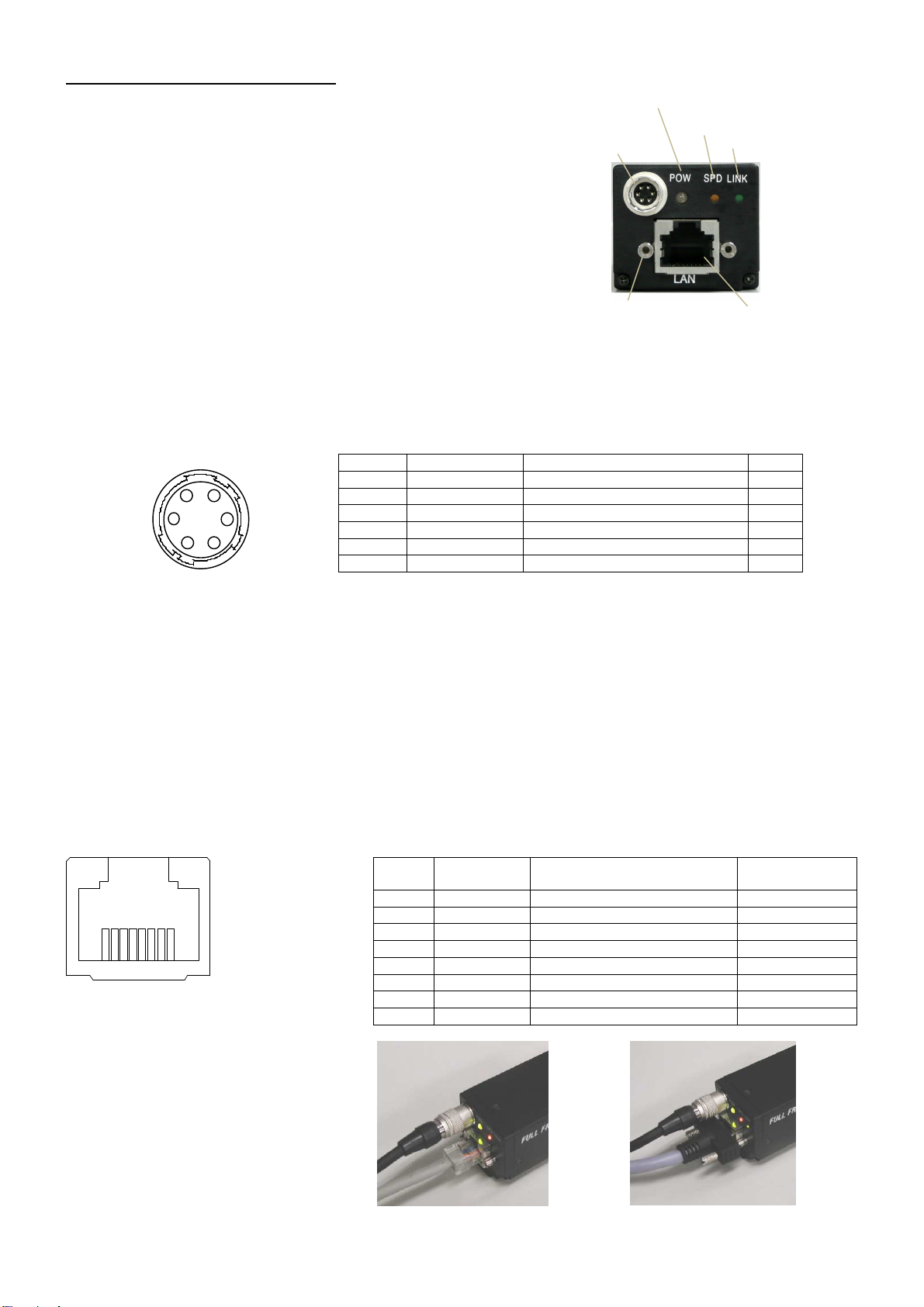
M11517;9/57
- 9 -
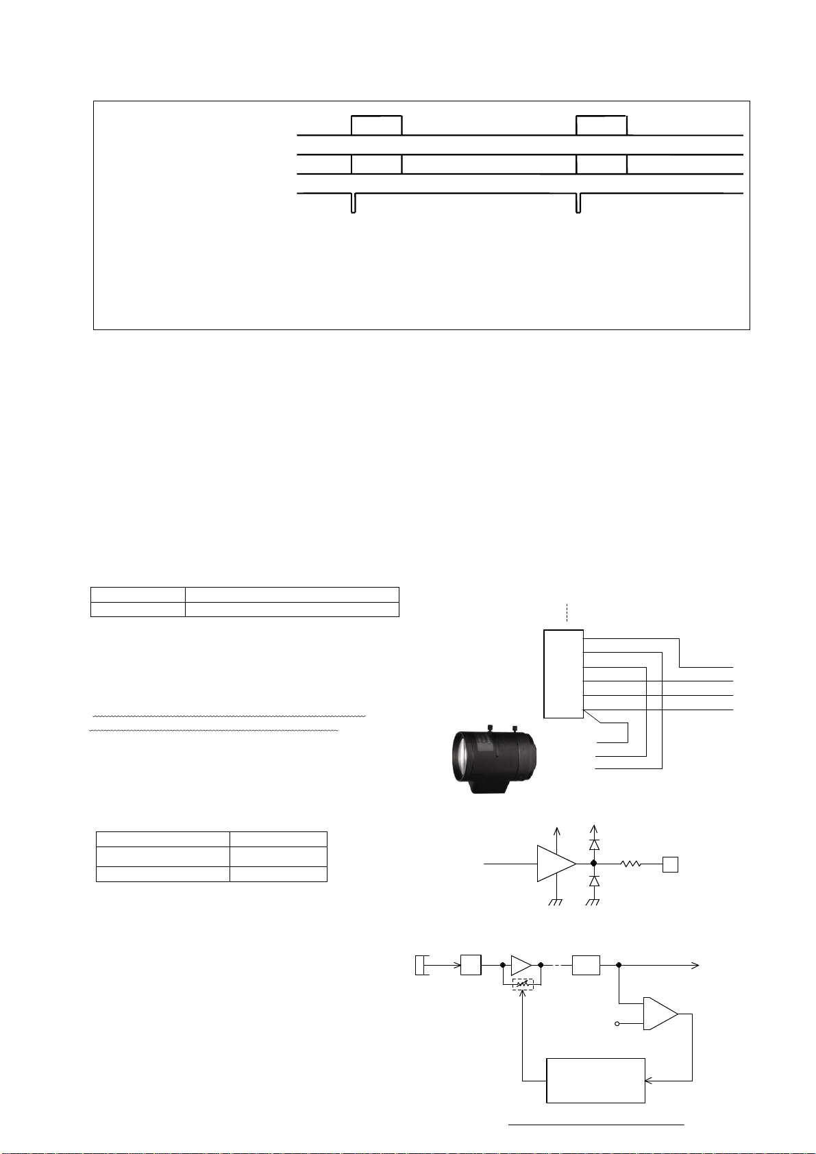
●Recommended timing of asynchronous shutter trigger signal (Vinit signal) for preset shutter/pulse width control
For the case of preset shutter mode
, the negative logic pulse is
applied within the width range from 1 H (1 horizontal synchronous
interval) to 1ms as described below.
For this
operation starts in synchronization with the trailing edge
the internal HD pulse
(the leading edge of pixel clock in the
case of H-reset mode)
after and closest to the trailing edge
timing of the applied pulse.
For the case of the pulse width control exposure mode,
value of
the L level interval of the input Vinit pulse (shown as Tvinit
in the figure) is retrieved in synchronization with the trailing edge
of the internal HD pulse (the leading
edge of pixel clock in the
case of H-reset mode)
, and the integer multiple number of H (1
horizontal synchronous interval) that is closest to the retrieved
Vinit pulse duration is transmitted as nH
number of pixel clock in the case of H-reset mode)
the camera. Then the shutter speed
is determined in response to
the time nH.
Vinit
Tvinit
[For the case of preset shutter mode]
1H ≤Tvinit ≤1ms
(The exposure time is independent of the Vinit width.)
[For the case of pulse width control mode]
(Where PWC=ENABLED, shutter switch = 9)
nH ≤Tvinit <(n+1)H (n is 1 or larger integer.)
(This is the pulse width where shutter exposure time =nH)
Recommended Vinit signal timing waveform
(Note) In the pulse width control, the shutter exposure time is almost equal to the integral multiple number of the
horizontal synchronous time (H) that is closest to the Vinit pulse duration. More specifically, however, the
shutter exposure time is indefinite for the time period corresponding to 1H width in the case of normal external
trigger input (or the case where the Vinit signal is not in synchronization with the horizontal synchronous
timing of the camera). It is improved by being employed in “with H-reset” mode
→Refer to the timing chart described in another section for the details.
(Note) When the shutter exposure time is too long in the pulse width control mode, the S/N ratio of the image will
be degraded due to the reduction of dynamic range of CCD, accumulation of thermal noise components of
CCD image sensor in proportion to the shutter speed and other factors. Therefore, if a long exposure time is
employed, it is recommended to conduct experiments using realistic exposure times in actual conditions to
check for the appropriateness.
●Example of drive circuit for Vinit input circuit
* The Vinit signal should not include unnecessary noise components such as chattering.
[Input voltage range]
H level 2.5 to 5.5 V
L level -0.5 to 0.5 V
*
T
he voltage of the terminal end on camera side is required to be within the above voltage range with the camera being connected.
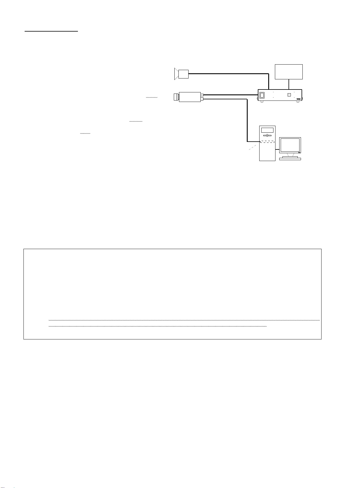
(4-5) Strobe signal (STRB)
It is able to adjust the light emitting timing of external strobe light to the exposure time of the camera.
This signal can be output in the continuous shutter mode as well as in the asynchronous shutter mode.
●Strobe signal output circuit
The signal output terminal is used both for strobe signal (STRB)
and busy (BUSY) signal.
Select any of OFF (Default: H level fixed), STRB and BUSY in
configuration setting.
→Refer to (7-5) Internal flag register and configuration register
The internal output circuit is shown in the right figure.
[output voltage range]
H level 3.0V (at 0mA) to 2.0 V (at 10mA)
L level 0.2V (at 0mA) to 0.5 V (at 10mA)
(!) The factory default is set to OFF for this camera.
It is required to set STRBC0 flag and STRBC1 flag when outputting STRB or BUSY signal,
●Output signal switching at strobe signal terminal
The signal from this terminal is set to OFF
as a factory default value.
This can be changed to STRB (Strobe timing
signal) or BUSY state by way of rewriting the
configuration register(CR) with serial
communication commands.
(CR5) and (CR6) correspond to STRBC0 and STRBC1, respectively.
(STRBC1,STRBC0)
Signal name Remarks
(0,0) OFF Always H level(Default)
(0,1) STRB Strobe timing
(1,0) BUSY Asynchronous shutter busy
100
5
STRB signal
or equivalent
internal circuit
Camera
connector
4
Vi ni t1 IN
VCC
4 7p
3.3 V
1 0k
T C7SH 14 FU o r equ ivalen t
To in te rn al c irc ui t
6.8V Z D
Trig ge r sign al v ia s eria l c o m m unic ation
Trig ger signal of inte rnal CPU origin
V C C is + 3.3V to +5 V
others
[Ex am p le of us e r circ u it]
Ins id e o f c am e ra