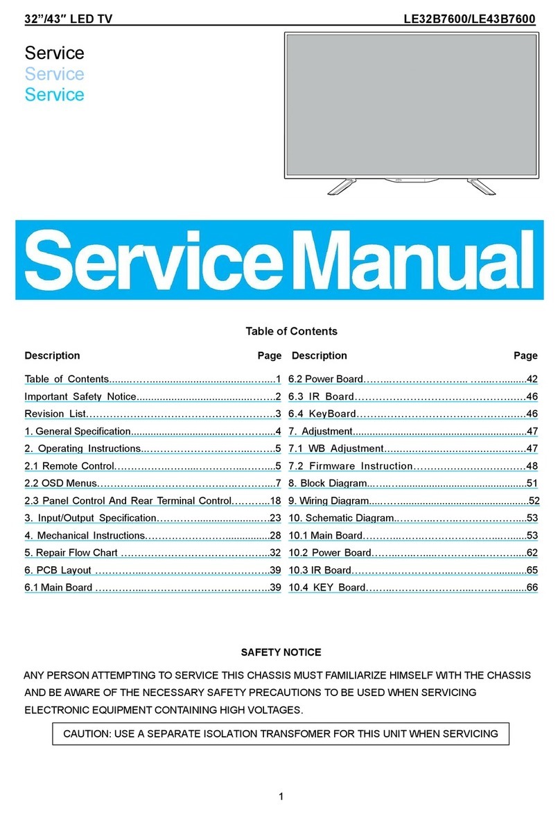
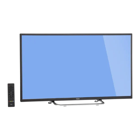
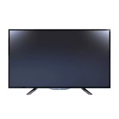
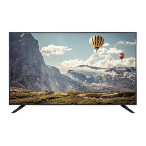
Haier LE39B8550T User manual

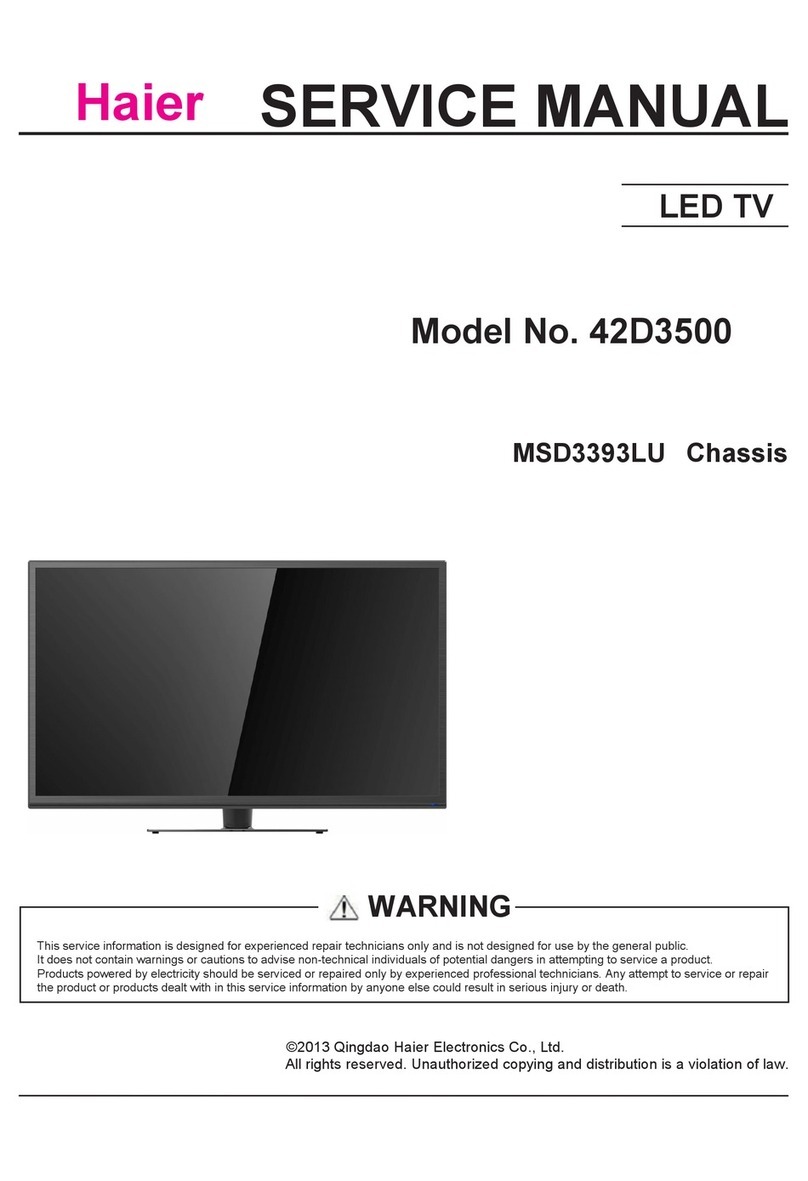
SERVICE MANUAL
LED TV
Chassis
MSD34631
This service information is designed for experienced repair technicians only and is not designed for use by the general public.
It does not contain warnings or cautions to advise non-technical individuals of potential dangers in attempting to service a product.
Products powered by electricity should be serviced or repaired only by experienced professional technicians. Any attempt to
service or repair the product or products dealt with in this service information by anyone else could result in serious injury or death.
WARNING
LE39B8550T
Model No.

1-1. Table of Contents
1. General Information...........................................................................
1-1. Table of Contents
1-3. Important Notice
1
Chapter 1: General Information
1
3
1-2. General Guidelines
1-4. How to Read this Service Manual
3
5
6SHFL¿FDWLRQV....................................................................................
Service Manual
Model No.:
- 01 -
3. Location of Controls and Components...........................................
3-1. Board Location
3-2. Main Board
4. Disassemble and Assemble..........................................................
4-1 Remove the Stand Base
6
7
7
7
11
11
4-2 Remove the Back Cover 11
4-3 Remove the Adhesive Tape 11
4-4 Remove the Main Board 12
4-5 Remove the Speaker 12
4-6 Remove the Remote Control Board 13
5. Installation Instructions..…....………………...........………….........14
5-1 External Equipment Connections 14
6. Electrical Parts…....………………...........…………......................... 15
6-2. Circuit Diagram
6-3. Wiring Connection Diagram
16
25
3-3. LED Panel 9
6-1. Block Diagram 15
7
3-4. Connector Definition 10
7. Trouble Shooting....………………...........…………....................... 26
7-1. Simple Check 26
7-2. Mainboard failure check 27
7-3. Panel Failure 35

1-2. General Guidelines
When servicing, observe the original lead dress. If a short circuit is found, replace all parts
which have been overheated or damaged by the short circuit.
After servicing, see to it that all the protective devices such as insulation barriers, insulation
papers shields are properly installed.
After servicing, make the following leakage current checks to prevent the customer from
being exposed to shock hazards.
1) Leakage Current Cold Check
2) Leakage Current Hot Check
3) Prevention of Electro Static Discharge (ESD) to Electrostatically Sensitive
1-3. Important Notice
1-3-1. Follow the regulations and warnings
Most important thing is to list up the potential hazard or risk for the service personnel to
open the units and disassemble the units. For example, we need to describe properly
how to avoid the possibility to get electrical shock from the live power supply or charged
electrical parts (even the power is off).
This symbol indicates that high voltage is present inside.It is dangerous to
make any king of contact with any inside part of this product.
This symbol indicates that there are important operating and maintenance
instructions in the literture accompanying the appliance.
1-3-2. Be careful to the electrical shock
7RSUHYHQWGDPDJHZKLFKPLJKWUHVXOWLQHOHFWULFVKRFNRU¿UHGRQRWH[SRVHWKLV79VHW
to rain or excessive moisture. This TV must not be exposed to dripping or splashing water,
DQGREMHFWV¿OOHGZLWKOLTXLGVXFKDVYDVHVPXVWQRWEHSODFHGRQWRSRIRUDERYHWKH79
1-3-3. Electro static discharge (ESD)
Some semiconductor (solid state) devices can be damaged easily by static electricity. Such
components commonly are called Electrostatically Sensitive (ES) Devices. The following
techniques should be used to help reduce the incidence of component damage caused by
electros static discharge (ESD).
1-3-4. About lead free solder (PbF)
This product is manufactured using lead-free solder as a part of a movement within the
consumer products industry at large to be environmentally responsible. Lead-free solder
must be used in the servicing and repairing of this product.
8VHWKHJHQHZLQJSDUWVVSHFL¿HGSDUWV
Special parts which have purposes of fire retardant (resistors), high-quality sound
(capacitors), low noise (resistors), etc. are used.
When replacing any of components, be sure to use only manufacture's specified parts
shown in the parts list.
Safety Component
Ɣ&RPSRQHQWVLGHQWL¿HGE\PDUNKDYHVSHFLDOFKDUDFWHULVWLFVLPSRUWDQWIRUVDIHW\
Service Manual
Model No.:
- 02 -

1-3-6 Safety Check after Repairment
- 03 -
Service Manual
Model No.:
&RQ¿UPWKDWWKHVFUHZVSDUWVDQGZLULQJZKLFKZHUHUHPRYHGLQRUGHUWRVHUYLFHDUHSXW
in the original positions, or whether there are the positions which are deteriorated around
the serviced places serviced or not. Check the insulation between the antenna terminal or
external metal and the AC cord plug blades. And be sure the safety of that.
General Servicing Precautions
1. Always unplug the receiver AC power cord from the AC power source before;
a. Removing or reinstalling any component, circuit board module or any other receiver
assembly.
b. Disconnecting or reconnecting any receiver electrical plug or other electrical
connection.
c. Connecting a test substitute in parallel with an electrolytic capacitor in the receiver.
CAUTION: A wrong part substitution or incorrect polarity installation of electrolytic
capacitors may result in an explosion hazard.
2. Test high voltage only by measuring it with an appropriate high voltage meter or other
voltage measuring device (DVM, FETVOM, etc) equipped with a suitable high voltage
probe.
Do not test high voltage by "drawing an arc".
5. Do not defeat any plug/socket B+ voltage interlocks with which receivers covered by this
service manual might be equipped.
8VHZLWKWKLVUHFHLYHURQO\WKHWHVW¿[WXUHVVSHFL¿HGLQWKLVVHUYLFHPDQXDO
CAUTION: 'RQRWFRQQHFWWKHWHVW¿[WXUHJURXQGVWUDSWRDQ\KHDWVLQNLQWKLVUHFeiver.
3. Do not spray chemicals on or near this receiver or any of its assemblies.
4. Unless specified otherwise in this service manual, clean electrical contacts only by
applying the following mixture to the contacts with a pipe cleaner, cotton-tipped stick or
comparable non-abrasive applicator; 10% (by volume) Acetone and 90% (by volume)
isopropyl alcohol (90%-99% strength).
CAUTION:7KLVLVDÀDPPDEOHPL[WXUH
8QOHVVVSHFL¿HGRWKHUZLVHLQWKLVVHUYLFHPDQXDOOXEULFDWLRQRIFRQWDFWVLVQRWUHTXLUHG
Capacitors may result in an explosion hazard.
6. Do not apply AC power to this instrument and/or any of its electrical assemblies unless
all solid-state device heat sinks are correctly installed.
7. Always connect the test receiver ground lead to the receiver chassis ground before
connecting the test receiver positive lead.
Always remove the test receiver ground lead last. Capacitors may result in an explosion
hazard.
9. Remove the antenna terminal on TV and turn on the TV.
10. Insulation resistance between the cord plug terminals and the eternal exposure metal
should be more than Mohm by using the 500V insulation resistance meter.
11. If the insulation resistance is less than M ohm, the inspection repair should be required.
If you have not the 500V insulation resistance meter, use a Tester. External exposure
metal: Antenna terminal Headphone jack
Service Manual
Model No.:
- 04 -
Electrostatically Sensitive (ES) Devices
1-3-7. Ordering Spare Parts
1. Immediately before handling any semiconductor component or semiconductor-
equipped assembly, drain off any electrostatic charge on your body by touching a known
earth ground. Alternatively, obtain and wear a commercially available discharging wrist
strap device, which should be removed to prevent potential shock reasons prior to applying
power to the unit under test.
2. After removing an electrical assembly equipped with ES devices, place the assembly
on a conductive surface such as aluminum foil, to prevent electrostatic charge buildup or
exposure of the assembly.
'RQRWXVHIUHRQSURSHOOHGFKHPLFDOV7KHVHFDQJHQHUDWHHOHFWULFDOFKDUJHVVXI¿FLHQW
to damage ES devices.
7. Immediately before removing the protective material from the leads of a replacement
ES device, touch the protective material to the chassis or circuit assembly into which the
device will be installed.
CAUTION: Be sure no power is applied to the chassis or circuit, and observe all other
safety precautions.
3. Use only a grounded-tip soldering iron to solder or unsolder ES devices.
Some semiconductor (solid-state) devices can be damaged easily by static electricity.
Such components commonly are called Electrostatically Sensitive (ES) Devices.
Examples of typical ES devices are integrated circuits and some field-effect transistors
and semiconductor "chip" components. The following techniques should be used to help
reduce the ncidence of component damage caused by static by static electricity.
4. Use only an anti-static type solder removal device. Some solder removal devices not
FODVVL¿HGDVDQWLVWDWLFFDQJHQHUDWHHOHFWULFDOFKDUJHVVXI¿FLHQWWRGDPDJH(6GHYLFHV
6. Do not remove a replacement ES device from its protective package until immediately
before you are ready to install it.
(Most replacement ES devices are packaged with leads electrically shorted together by
conductive foam, aluminum foil or comparable conductive material).
8. Minimize bodily motions when handling unpackaged replacement ES devices.
(Otherwise harmless motion such as the brushing together of your clothes fabric or the
OLIWLQJRI\RXUIRRWIURPDFDUSHWHGÀRRUFDQJHQHUDWHVWDWLFHOHFWULFLW\VXI¿FLHQWWRGDPDJH
an ES device.)
Please include the following informations when you order parts. (Particularly the Version
letter)
1. Model number, Serial number and Software Version
The model number and Serial number can be found on the back of each product and the
Software Version can be found at the Spare Parts List.
2. Spare Part No. and Description
<RXFDQ¿QGWKHPLQWKH6SDUH3DUWV/LVW

- 05 -
Service Manual
Model No.:
1-3-8. Photo used in this manual
The illustration and photos used in this Manual may not base on the final design of
products, which may differ from your products in some way.
1-4. How to Read this Service Manual
Using Icons:
,FRQVDUHXVHGWRDWWUDFWWKHDWWHQWLRQRIWKHUHDGHUWRVSHFL¿FLQIRUPDWLRQ7KHPHDQLQJRI
each icon is described in the table below:
Note:
A “note” provides information that is not indispensable, but may nevertheless be valuable
to the reader, such as tips and tricks.
Caution:
A “caution” is used when there is danger that the reader, through incorrect manipulation,
may damage equipment, loose data, get an unexpected result or has to restart(part of) a
procedure.
Warning:
A “warning” is used when there is danger of personal injury.
Reference:
A “reference” guides the reader to other places in this binder or in this manual, where he/
VKHZLOO¿QGDGGLWLRQDOLQIRUPDWLRQRQDVSHFL¿FWRSLF

Service Manual
Model No.:
- 06 -
6SHFL¿FDWLRQV
Model LE39B8550T
Screen Size31.5 inch
Aspect Ratio 16:9
Resolution 1366*768
Response Time (ms) (GRAY TO
GRAY)
Angel ofView
Color Display16.7M
No. ofPreset Channels
OSD LanguageEn
Color SystemPAL/SECAM
Audio SystemDK, BG, I
Audio Output Power
(Built-in) (W) 8W×2
Audio Output Power
(outer) (W) No
Total Power Input (W) 45W
Voltage Range (V)
Power Frequency (Hz) 50~60Hz
AC 100-240V
500(DTV);100(ATV)
160°/150°
20
glish, Russian

- 07 -
Service Manual
Model No.:
3. Location of Controls and Components
3-1 Board Location
No. Description
ABoard Integration Mainboard
3-2 Main Board
ABoard

Service Manual
Model No.:
- 08 -
3-2-1 Function Description:
Main Board
Process signal which incept from exterior equipment then translate into signal that panel
can display.
&RQQHFWRUGH¿QLWLRQ
Main board connector
Pin number Signal name Description
1 RSPK+ RSPK+
2 RSPK- RSPK-
3 LSPK- LSPK-
4 LSPK+ LSPK+
Keypad and remote connector ( CN201 )
3LQQXPEHU 6LJQDOQDPH 'HVFULSWLRQ
/('B5 /$035('
/('B* /$03*5((1
,5 5(027(&21752/
*1' *1'
9 32:(5)255(027(
1&
.(<
*1'
9
1&
STANDBY
Speaker connector (CN601)

3-3. LED Panel
- 09 -
Service Manual
Model No.:
SAM LSC320AN09-H

Service Manual
Model No.:
- 10 -
3-4.Connector Definition

4. Disassemble and assemble
Remove the adhesive tape indicated on the
¿JXUHDERYH
/D\GRZQWKHXQLWVRWKDWUHDUFRYHU
faces upward
5HPRYHWKHVFUHZIURPWKH
UHDUFRYHULQGLFDWHGZLWKż
7KHQUHPRYHWKHSHGHVWDO
4-2 Remove the Back Cover
5HPRYHWKHVHVFUHZLQGLFDWHGRQ
¿JXUHDERYHE\ż
7KHQUHPRYHWKHEDFNFRYHUIURPWKH
unit.
Service Manual
Model No.:
- 11 -
4-1 Remove the Stand Base
4-3. Remove the adhesive tape

4-4 Remove the Main board
5HPRYHWKH0DLQERDUG
Service Manual
Model No.:
- 12 -
'LVFRQQHFWHGWKHFRXSOHU
4-5 Remove the speaker
Take out the speaker

4-6 Remove the remote control board
take out the remote control
board
Service Manual
Model No.:
- 13 -

5. Installation Instructions
5-1 External Equipment Connections
Service Manual
Model No.:
- 14 -
Accessories
Remote control refers to user manual.Remote control refers to user manual.

5
5
4
4
3
3
2
2
1
1
D D
C C
B B
A A
YUV
AMP
MHL
+3.3V/670MA
DVD_L/R
PU2
UD8 Q101
11Ω-4A-0603
UD7
U107
DD401
QD6
UD3 +12V/1.65A
SCARTX1 SCART
CI
SPDIF
AV OUT
100V~240V
AC POWER IN
EARPHONE
L
R
BL
+24VB
MOS 3401 +3.3V_Normal/150MA
+12VB
HDMI1(ARC)
MSD3463GS
HDMI2
HDMI
输入
X2
YUVI
输入
X1
VGA
输入
X1 VGA
AVAV
输入
X1
TUNE
输入
USB1
USB
输入
X1
VGA_L/R
YUV_L/R
SCART_L/R
音频输入
X2 AV
音视频
输出
AV_OUT
L/R_OUT
遥控接收、键控板
光感接收、指示板
PANLELVDS
IF1
IF2
IF
MP7751
L
R
L_OUT
R_OUT
SPI FLASH
16MBITS
+12V_Normal/3A
+12VB
TPS563201/3A +5V_Standby/3A
+12VB
OB6220/TPA3136
TPS563201/3A +1.2V_VDDC/3A
TLV62565/1.5A +3.3V_Standby/320MA
+1.5V_DDR/220MA
TLV62565/1.5A
MOS
AO3407 VCC_Pannel /1.5A
MSD3463GS
L511
3.3V_TUNER/200MA
FUSE 5V_USB/1A
PWR_ON/OFF
PWR_ON/OFF
PWR_ON/OFF
+12VB
POWER BOARD
NAND_FLASH
1GBITS
Title
Size Document Number Rev
Date: Sheet of
Change list
1.0
MSD3643GSA
Custom
110Tuesday, October 11, 2016
Title
Size Document Number Rev
Date: Sheet of
Change list
1.0
MSD3643GSA
Custom
110Tuesday, October 11, 2016
Title
Size Document Number Rev
Date: Sheet of
Change list
1.0
MSD3643GSA
Custom
110Tuesday, October 11, 2016
MTC-34631-SCH
6-1. Block Diagram6-1. Block Diagram

5
5
4
4
3
3
2
2
1
1
D D
C C
B B
A
A
新增
5V Max@DTV(with out CI,USB,DVD,panel)490mA
5V Stb(with out ci card)23mA
CI card module max 200mA
新增
down
up
V =0.768X(1+R /R )
out
2012-11-6
改善低温
-10oC
不启动
D809
由
1N4007
改为
FR107
2013-5-11
LF800
长虹要求
EMC 6dB
余量
单独修改
M29
组件
2012-8-1
RV1
位置
DCN
统一改为
561
2012-10-25
欧规组件统一改为
450V
耐压
2013-5-23
美国市场改为
400V
耐压
C1053
跟公板
BOM
不对
公板
BOM 10uF/50
老化端口
H:ON
L:OFF
Vout=2×
(
PR45+PR47
)
/PR47
一般需要固定
R826
,只改
PR47
,
否则会影响到输出功率。
TO INVERTER
额定电流
/
工作电流
4A/1.08A
额定电流
/
工作电流
4A/1.08A
工作频率
477Khz
占空比
43%
工作电流
1.1A,
实测电压
5.16V,
纹波
100mV
ON/BK
+12V
+5V_Standby
24V
24V
+12V
24V
LED+
ON/BK
OVP
DRV
LED+
DRV
+12V
CS
FB FB1
FB
FB1
+12V_PD3
OVP
EN
BL-ADJUST
LED1
LED+
BL-ADJUST
BKLON
ON/BK
BL-ADJUST
BKLONBKLON
BKLONBKLONBKLON
5Vstb
+12V
+5V_Standby
+3.3V_Normal
+3.3V_Normal
+12V_Normal
+12V_Normal
+3.3V_Standby
+5V_Normal
+5V_Standby
+12V_Normal
VBL_CTRL 4
BRI_ADJ4
PWR_ON/OFF 10,3,4
OP_ON/OFF
10,3
Title
Size Document Number Rev
Date: Sheet of
Change list
1.0
MSD3643GSA
Custom
210Friday, December 02, 2016
Title
Size Document Number Rev
Date: Sheet of
Change list
1.0
MSD3643GSA
Custom
210Friday, December 02, 2016
Title
Size Document Number Rev
Date: Sheet of
Change list
1.0
MSD3643GSA
Custom
210Friday, December 02, 2016
32
1
102PF-1KV
+
2 1
1
2
3
+
2 1
2 1
12
+
1
2
+
1
2
+
12
NP2
NP1
NB1
NB2
NP2
12V 6
5V 2
12V 7
5V 3
GND 5
10
10
NC
11
12
12
8
8
9
9
GND 4
NC 1
12
43
+
12
GATE
2
VIN
1
GND
3
CS
4FB 5
CMP 6
OVP 7
PWM 8
1
2
GND
1
RI
3
CS 4
VDD 5
GATE 6
FB
2
CD94
10uF/6.3V/X5R/0603
1
2
3
4
1
2
+
22
1
1
3
3
+
22
1
1
3
3
NP2
NP1
NB1
NB2
NP2
12V 7
12V 9
GND 8
3
3
2
2
1
1
5
5
6
6
24V 10
+
1
2
3
TPS563201
SOT23-6
GND
1
LX 2
VIN
3
FB 4
EN
5
BS 6
+
4
2 1
3
+
1
2
MTC-34631-SCH
6-2. Circuit Diagram6-2. Circuit Diagram

5
5
4
4
3
3
2
2
1
1
D D
C C
B B
A A
Vpp=100mV
PANEL POWER
1.2V 3A for VDDC
down
up
V =0.768X(1+R /R )
out
811MA
1.5V Power for DDR3
<1A 5V Input--->Output 1.5V
<1A 5V Input--->Output 3.3V
410MA
3.3V DC-DC
电流
390mA 3.28V
3.3V Normal Power MARK
工作频率
1.398Mhz
占空比
30%
工作电流
234mA,
实测电压
1.54V,
纹波
50mV
工作频率
474Khz
占空比
10%
工作电流
800mA,
实测电压
1.16V
,纹波
35mV
工作频率
1.352Mhz
占空比
65%
工作电流
498mA,
实测电压
1.32V,
纹波
24mV
PWR_ON/OFF
OP_ON/OFF
+12V_Normal
+5V_Normal
VCC-PanelVCCLCDFN
VCCLCDFN
1.2V_VDDC
+12V_Normal
+5V_Normal
+1.5V_DDR
+5V_Standby
+3.3V_Standby
+3.3V_Standby
+3.3V_Normal
+5V_Standby
1.2V_VDDC
+3.3V_Normal
PANEL_ON/OFF4
PWR_ON/OFF 10,2,4
OP_ON/OFF 10,2
Title
Size Document Number Rev
Date: Sheet of
Change list
1.0
MSD3643GSA
Custom
310Tuesday, October 11, 2016
Title
Size Document Number Rev
Date: Sheet of
Change list
1.0
MSD3643GSA
Custom
310Tuesday, October 11, 2016
Title
Size Document Number Rev
Date: Sheet of
Change list
1.0
MSD3643GSA
Custom
310Tuesday, October 11, 2016
RD60
10K
C150 10uF/6.3V/X5R/0603
CD101 10uF/6.3V/X5R/0603
RD59 NC/0R/0805
R135
47K/1%
TLV62561
UD7
IC-DCDC/TLV62565/1.5A,5.5V,
降压
/SOT23-5
GND
2
LX 3
VIN
4
OUT/FB 5
EN
1
C118 10uF/25V/X5R/0805
RD64
4.7K
RD141
120K/1%
RD63
4.7K
C107 0.1uF/16V/X7R
TLV62561
UD8
IC-DCDC/TLV62565/1.5A,5.5V,
降压
/SOT23-5
GND
2
LX 3
VIN
4
OUT/FB 5
EN
1
C111 10uF/25V/X5R/0805
C126
1000PF/50V/X7R
CD102 10uF/6.3V/X5R/0603
RD66
4.7K
RD65
4.7K
C151 0.1uF/16V/X7R
R103
68K
RD56 0R/0805
R3
2.2K-0603
LD21
2.2uH_2A
C117
10nF/50V/X7R
RD62 270K
QD6 A03407
C106 10uF/6.3V/X5R/0603
H2
NC
1
2
3
4
5
6
7
8
9
CD86 0.1uF/16V/X7R
L101 2.2uH-2.5A
C122 33PF/50V/NPO
CD104
100pF/50V/NPO
LD22 2.2uH_2A
RD145
75K/1%
T1
NC
1
2
3
4
5
6
7
8
9
RD144
100K/1%
C113 10uF/6.3V/X5R/0603
C105 10uF/6.3V/X5R/0603
R108
100K
C134 10uF/6.3V/X5R/0603
CD103
100pF/50V/NPO
R112 68K
C125 1uF/25V/X5R/0603
Q101
MOS-P/KO3401, 4.2A,30V,±12V,SOT-23 KEXIN
C138 10uF/6.3V/X5R/0603
R134
10K/1% CD96
10uF/6.3V/X5R/0603
CD88 0.1uF/16V/X7R
C124
NC/33PF
R136
100K/1%
R109 220R/0603
CD97 NC/10uF/6.3V/X5R/0603
CD93 NC/10uF/6.3V/X5R/0603
CD87 10uF/6.3V/X5R/0603
+
EC105 NC/220uF/10V
QD10
3904
3
1
2
CD91 10uF/6.3V/X5R/0603
CD85
10uF/6.3V/X5R/0603
CD53
0.22uF/16V/X5R
C123 NC/33PF
QD7
3904
3
1
2
H3
NC
1
2
3
4
5
6
7
8
9
RD136
220K/1%
C112
0.1uF/16V/X7R
RD140
100K
TPS563201
SOT23-6
U107
IC-DCDC/TPS563201,3A,17V,SOT23-6
,
0.75V TI
GND
1
LX 2
VIN
3
FB 4
EN
5
BS 6
RD135
100K/1%
RD139
51K/1%
H1
NC
1
2
3
4
5
6
7
8
9
MTC-34631-SCH

5
5
4
4
3
3
2
2
1
1
D D
C C
B B
A A
MHL Port
SAR1-->
SC-HSYNC
Transport Stream
CORE POWER DDR3 POWER
Standby Power 3.3V
SPI NOR FLASH
RESET
IC Configuration Selection
Audio Line OUT
AV/SCART
共用声音输出
Audio Line Out
Audio Line IN
YPBPR/AV/VGA
共用声音输入
VGA
SCART
YPBPR
AV
AUDIO LINE IN
CVBS OUT
SPDIF OUT
HDMI
PCMCIA
LVDS
OTHER
CHIP_CONFIG[1:0]
{PAD_PWM1, PAD_PWM0}
2'b01 Boot from SPI_NOR Flash
2'b10 Boot from ROM
Close to MSTAR IC
with width trace
IF AGC
不能省掉!
close to IC
EEPROM
IC
根据实际电源
上电时序调整
KEYBOARD
FOR TEST
System XTAL
NOTE:
晶体频偏需要小于
30PPM
删除
1M
电阻!
公板为
100MHZ/150mA/1K
LED DEBUG_UART
MUST pull high to 5VSTB
ISP AND VGA EDID
D201
改用复位
IC
:
314SGM81001
,
相应变更:
1.
删除
R244,R247,Q201,C247
2.C276
,
R253
贴
0Ω__2016.07.09
HDMI_CEC
HDMI2_CLKN
HDMI2_HPDIN
HDMI2_RX0N
HDMI2_RX2P
HDMI2_RX1N
HDMI2_RX2N
HDMI2_RX1P
HDMI2_SDA
HDMI2_SCL
HDMI2_CLKP
HDMI2_RX0P
HDMI2_SDA
HDMI2_SCL
PCM_IOWR_N
PCM_OE_N
PCM_IORD_N
PCM_REG_N
PCM_CD_N
PCM_WE_N
PCM_IRQA_N
PCM_WAIT_N
PCM_CE_N
PCM_RESET
SPI_SDO#
UART-RX
UART-TX
SC-HSYNC
MHL_CABLE-DET
KEY0_IN
RXE2-
RXO1+
RXE1+
RXEC+
RXE3-
RXE4+
RXO4+
RXO0-
RXE0-
RXO4-
RXO3+
RXO0+
RXE0+
RXE2+
RXO1-
RXE1-
RXEC-
RXE3+
RXO2-
RXE4-
RXO2+
RXO3-
SPDIF-OUT
SC-CVBS-IN
SC-VSYNC
HDMI2_HPDIN
AVDD5V_MHL
ARC
HDMI_CEC
AMP-MUTE
HDMI1_SCL
HDMI1_SDA
HDMI1_HPDIN
HDMI1_RX2P
HDMI1_RX1N
HDMI1_RX2N
HDMI1_RX1P
HDMI1_CLKN
HDMI1_CLKP
HDMI1_RX0P
HDMI1_RX0N
VGA_VS
BIN0
RIN2
RIN0
GIN0M
GIN0P
VGA_HS
CVBS_OUT0
VCOM0
GIN2P
GIN2M
BIN2
CVBS0
HDMI2_CLKN
HDMI2_RX2P
HDMI2_RX1N
HDMI2_RX2N
HDMI2_RX1P
HDMI2_CLKP
HDMI2_RX0P
HDMI2_RX0N
PANEL_ON/OFF
VIFM
IFAGC_T
PWR_ON/OFF
PANEL_ON/OFF
TUNER_SCL
TUNER_SDA
BRI_ADJ-PWM0
IFAGC_S
TS0_SYNC
TS1_VLD
TS0_CLK
TS1_CLK
TS0_VLD
TS1_SYNC
TS1_D4
TS1_D5
TS1_D6
TS1_D7
TS1_D1
TS1_D2
TS1_D3
TS1_D0
GIN1M
BIN1
GIN1P
RIN1
VIFM
VIFP
IFAGC-T
XTALI
XTALO
IFAGC-S
MHL_CABLE-DET
ARC
IFAGC-T IFAGC_T
PCM_A14
PCM_A1
PCM_A6
PCM_A3
PCM_A2
PCM_A7
PCM_A4
PCM_A0
PCM_A5
PCM_A13
PCM_A9
PCM_A10
PCM_A11
PCM_A8
PCM_A12
TS0_D4
TS0_D6
TS0_D7
TS0_D1
TS0_D0
TS0_D5
TS0_D2
TS0_D3
PCM_D0
PCM_D2
PCM_D1
PCM_D7
PCM_D6
PCM_D5
PCM_D4
PCM_D3
AV-LINEOUTL
AV-LINEOUTR
IM_S
IP_S
DISEQC
VBL_CTRL
IFAGC-S IFAGC_S
VCOM0
CVBS0
SC-CVBS-IN
RIN2
BIN0
GIN0M
GIN0P
RIN0
VGA_HS
VGA_VS
GIN2P
GIN2M
BIN2
SC-HSYNC
SC-VSYNC
GIN1M
GIN1P
RIN1
BIN1
AV
CVBS_OUT0
AUR3
AUL3
AUR4
AUL4
SPDIF-OUT
AUVRM
AUVAG
VIFP
QP_S
IP_S
USB1_DP
USB1_DM
AUVRM
AUVAG
AUR4
AUR3
AUL3
AUL4
HDMI1_DEC
M-SCL
M-SDA
PCM_A14
PCM_A6
PCM_A1
PCM_A7
PCM_A2
PCM_A3
PCM_A5
PCM_A4
PCM_A9
PCM_A13
PCM_A8
PCM_A11
PCM_A10
PCM_A12
PCM_D3
PCM_D7
PCM_D6
PCM_D5
PCM_D4
PCM_D0
PCM_D2
PCM_D1
M-SDA
M-SCL
PWR_ON/OFF
HDMI1_DEC
DISEQC
PCM_IORD_N
PCM_OE_N
PCM_IOWR_N
PCM_WAIT_N
PCM_IRQA_N
PCM_REG_N
PCM_WE_N
PCM_CD_N
PCM_RESET
PCM_CE_N
VBL_CTRL
PCM_A0
TS0_D7
TS0_D6
TS0_D4
TS0_D0
TS0_D1
TS0_D3
TS0_D2
TS0_D5
AMP-MUTE
TS0_SYNC
TS1_SYNC
TS0_CLK
TS1_VLD
TS0_VLD
TS1_CLK
TS1_D4
TS1_D5
TS1_D6
TS1_D0
TS1_D1
TS1_D7
TS1_D2
TS1_D3
RXE3+
RXE3-
RXEC-
USB1_DP
USB1_DM
RXEC+
RXO4-
RXO4+
RXO0+
RXE1-
RXO0-
RXO1-
RXO1+
RXE2-
RXE0+
RXE0-
RXE1+
RXO2-
RXE2+
RXO2+
RXO3-
RXO3+
RXE4-
RXE4+
IR_SYNC
SPI_SDI#
SPI_CSN#
AV_ON-PWM1
System-RST
BRI_ADJ-PWM0
TUNER_SCL
TUNER_SDA
AMP-AUOUTL
AMP-AUOUTR
AV-LINEOUTR
AV-LINEOUTL
AMP-AUOUTR
AMP-AUOUTL
TS0_D[7:0]
TS1_D[7:0]
PCM_A[14:0] PCM_D[7:0]
BRI_ADJ-PWM0
AV_ON-PWM1
System-RST
IRIN
KEY0_INKEY0KEY0KEY0KEY0KEY0KEY0KEY0KEY0KEY0KEY0KEY0KEY0KEY0KEY0KEY0KEY0 KEY1-in
IRINIRIN
LED_R
LED_G
IR_SYNC
SPI_SCK
SPI_CSN SPI_CSN#
#F_WP
SPI_SDO
SPI_CSN
TP2
SPI_SCK
SPI_SDI
+3.3V_Standby
SPI_SDI#
SPI_SDO#
SPI_SDI
SPI_SDO
#F_WP
SPI_CSN
SPI_SDI
SPI_SCK
TP2
SPI_SDO
XTALOXTALI
MHL_VBUS-EN
MHL_VBUS-EN
QM_S
QP_S
AV_ON-PWM1
TP2
KEY1-in
HDMI1_SDA
HDMI1_SCL
HDMI1_HPDIN
HDMI1_CLKP
HDMI1_CLKN
HDMI1_RX0N
HDMI1_RX0P
HDMI1_RX1N
HDMI1_RX1P
HDMI1_RX2N
HDMI1_RX2P
PHDETEC
PHDETEC
SPI_SCK#
SPI_SCK#
AUR2
AUL2
AUL2
AUR2
LED_R
LED-G LED_G
LED-R
LED-R
LED-G
UART_RX UART-RX
UART-TXUART_TX
HDMI2-SDA
HDMI2-SCL
UART_RX HDMI2-SCL
UART_TXHDMI2-SDA
LCD_OP
LCD_OP
AVDD_EAR33
VDDC
VDDC
AVDD_MOD1
DVDD_DDR
AVDDL_DVI
AVDD_MOD
AVDD3P3_ADC
AVDD_DDR_DATA
AVDD_DDR_CMD
AVDD_DMPLL
VDDC
AVDD_DADC
AVDD_ETH
1.2V_VDDC AVDDL_DVI DVDD_DDRVDDC +1.5V_DDR AVDD_DDR_CMD AVDD_DDR_DATA
AVDD_MOD1
+3.3V_Standby AVDD_MOD
AVDD_AU33AVDD_EAR33 AVDD_DADC
+3.3V_Standby
AVDD3P3_ADC
AVDD_DMPLL
+3.3V_Standby
+3.3V_Standby
+3.3V_Normal
AVDD5V_MHL
+3.3V_Normal
AVDD_ETH
+3.3V_Standby
AVDD_AU33
AVDD_MOD
AVDD_DDR_CMD
VDDC
VDDC
AVDD_MOD
VDDC
+3.3V_Normal
+5V_Standby
+5V_Standby
+5V_Standby
+3.3V_Standby
+3.3V_Standby
+3.3V_Standby
+3.3V_Standby
+3.3V_Standby
+5V_Standby
HDMI2/5V
+5V_Standby
HDMI2_SCL 6
HDMI2_HPDIN 6
HDMI2_CLKN 6
HDMI2_SDA 6
HDMI_CEC 6
HDMI2_RX0P 6
HDMI2_RX1N 6
HDMI2_RX1P 6
HDMI2_RX0N 6
HDMI1_ARC 6
PCM_IOWR_N 9
PCM_OE_N 9
PCM_WAIT_N 9
PCM_CD_N 9
PCM_IORD_N 9
PCM_RESET 9
PCM_A[14:0]
11,9
PCM_IRQA_N 9
PCM_WE_N 9
PCM_CE_N 9
PCM_REG_N 9
PCM_D[7:0]
9
PWR_ON/OFF 10,2,3
RXE_0+ 5
RXE_0- 5
IFAGC_S 8
RXE_2- 5
RXE_1+ 5
RXE_1- 5
RXE_C+ 5
RXE_C- 5
RXE_2+ 5
RXE_4- 5
RXE_3+ 5
RXE_3- 5
RXE_4+ 5
RXO_0+ 5
RXO_0- 5
RXO_2- 5
RXO_1+ 5
RXO_1- 5
RXO_3- 5
RXO_2+ 5
RXO_4+ 5
RXO_4- 5
RXO_3+ 5
AMP_MUTE 7
MHL_CABLE_DET
6
MHL_VBUS_EN 6
HDMI1_RX0N 6
HDMI1_RX0P 6
HDMI1_RX2P 6
HDMI1_RX1N 6
HDMI1_RX1P 6
HDMI1_CLKN 6
HDMI1_CLKP 6
HDMI1_RX2N 6
HDMI1_SDA 6
HDMI1_SCL 6
HDMI1_HPDIN 6
VIFM 8
VIFP 8
BRI_ADJ 2
PANEL_ON/OFF 3
TUNER_SCL 8
TS1_D[7:0] 9
TS0_D[7:0] 9
TS1_CLK 9
TS0_SYNC 9
TS0_VLD 9
TS0_CLK 9
TS1_SYNC 9
TS1_VLD 9
IFAGC_T 8
HDMI2_CLKP 6
HDMI2_RX2N 6
HDMI2_RX2P 6
AMP_AUR 7
AV-AUOUTR0 10
AV-AUOUTL0 10
QP_S_1 8
IP_S_1 8
DISEQC 8
VBL_CTRL 2
AV 10
YPbPr-PB 10
YPbPr-PR 10
SCART-AV-IN 10
SCART-FB 10
SCART-FS 10
YPbPr-Y 10
SCART-G 10
SCART-R 10
SCART-B 10
VGA-HSYNC 10
VGA-VSYNC 10
VGA-B 10
VGA-G 10
VGA-R 10
CVBS_OUT0 10
AV-LIN 10
AV-RIN 10
SCART-RIN 10
SCART-LIN 10
SPDIF_OUT 10
TUNER_SDA 8
USB1_DP 10
USB1_DM 10
AMP_AUL 7
HDMI1_DEC 6
AV_ON-PWM1 10
HP_DET 8
VGA-Rin_AU 10
VGA-Lin_AU 10
HDMI2_SDA 10,5
HDMI2_SCL 10,5
UART_TX
10
UART_RX
10
LCD_OP 5
Title
Size Document Number Rev
Date: Sheet of
Change list
1.0
MSD3643GSA
Custom
410Tuesday, October 11, 2016
Title
Size Document Number Rev
Date: Sheet of
Change list
1.0
MSD3643GSA
Custom
410Tuesday, October 11, 2016
Title
Size Document Number Rev
Date: Sheet of
Change list
1.0
MSD3643GSA
Custom
410Tuesday, October 11, 2016
C244
0.1uF
FB205
0R
C221 2.2uF
CD50
100pF/50V/NPO
Q6
3904
1
23
R237 NC/1M
R248 1K
C220 2.2uF
R229 0R
R226 NC/1K
C280
0.1uF
R242
27R-1206
C209 47nF
C241
0.1uF
R216 180R
R234 10K
C276
2.2uF
FB207
100MHZ/300mA/600R
C144 10P
C108
NC/10uF/6.3V/X5R/0603
C206 47nF
C225
1nF
7531
8642
RP40 56RX4
C234
10uF
C245
2.2uF
C259
2.2uF
C263
22nF
C288
0.1uF
C322
0.1uF
C228 2.2uF
R261
NC/4.7K
R220 430R
C205 47nF
C202 47nF
RD185
4.7K
R262
NC/4.7K
C277
1nF
CN201
10PIN-2.0
1
12
23
34
45
56
67
78
89
910
10
R210 33R
R203 33R
C246
0.1uF
R236 0R
R207 33R
C204 47nF
C252
0.1uF
R253
0/NC
C262
22nF
RD49 1K
C216 47nF
C323
0.1uF
R223 10K
R201 33R
C208 47nF
R204 33R
C239
0.1uF
C110
NC/10uF/6.3V/X5R/0603
R2
4.7K
UD1
1
2
C275
0.1uF(X7R)
R275 2.2K
C147 0.1uF(X7R)
R282 2.2K
R249
100K
C266
12pF/50V/NPO
C289
0.1uF
C232
0.1uF
RD44
4.7K
C291
0.1uF
R246
NC/4.7K
C201 47nF
C207 47nF
R215 150R
FB209
100MHZ/300mA/600R
C243
0.1uF
FB212 0R
R221
4.7K
C223 2.2uF
C251
0.1uF
R251
4.7K
C238
0.1uF
R244
470K
R205 33R
R211 33R
R206 68R
R264
NC/10K
C249
10uF
FB201
150mA/1K
R213 33R
TF1
TP
TF1
1TF2
2TF3
3TF4
4TF5 5
TF6 6
TF7 7
TF8 8
Q201
3906
1
3 2
C214 47nF
C141
0.1uF(X7R)
R217 100R
RD53 1K
C253
0.1uF
C290
0.1uF
R219 4.7K
R209 68R
Q5
3904
1
2 3
C278
0.1uF
C267
12pF/50V/NPO
FB211
100MHZ/300mA/600R
U201
MX25L6405DMI-12G
(
SOP-8
)
CE#
1
SO
2
WP#
3
VSS
4SI 5
SCK 6
HOLD# 7
VDD 8
R247 10K
C235
0.1uF
C279
0.1uF
C2560.1uF
C274
10uF
R214 150R
R208 33R
R218 100R
C224 2.2uF
C226
1nF
R202 68R
FB202
100MHZ/300mA/600R
C143
10P
R263
NC/10K
C247
2.2uF
C236
10uF
Q7
3904
1
23
R227 10K
R224 NC/1K
CD47
33P
D201
BAV99
3
1
2
Y1
24MHz/DIP
RD184
4.7K
C212 47nF
C2580.1uF
C203 47nF
C213 47nF
C211 47nF
C240
0.1uF
MSD3463GSA
U202 MSD3463GSA
EPAD 217
RX0N_B
1
RX0P_B
2
RX1N_B
3
RX1P_B
4
RX2N_B
5
RX2P_B
6
AVDD_MOD
7
RXCN_A
8
RXCP_A
9
RX0N_A
10
RX0P_A
11
RX1N_A
12
RX1P_A
13
RX2N_A
14
RX2P_A
15
HSYNC0
16
BIN0P
17
GIN0P
18
GIN0M
19
RIN0P
20
VSYNC0
21
AVDD3P3_ADC
22
BIN1P
23
GIN1P
24
GIN1M
25
RIN1P
26
CVBS0
33
CVBS1
34
VCOM
35
CVBS_OUT1
36
VDDC
38
LINEIN_L2
42
LINEIN_R2
43
AUVRM
40
VAG
41
LINEIN_L4
46
LINEIN_R4
47
AVDD_AU33
39
LINEOUTR3
48
LINEOUTL3
49
EARPHONE_OUTL
50
EARPHONE_OUTR
51
AVDD33_EAR
52
QP_S
53
QM_S
54
AVDD3P3_DADC
55
IP_S
56
IM_S
57
IFAGC_S
58
IFAGC_T
59
IP_T
60
IM_T
61
AVDD3P3_DMPLL
62
XIN
63
XOUT
64
VDDC
66
GPIO44/TX1
67
GPIO45/RX1
68
PWR_ON/OFF
69
GPIO48/DISEQC
71
VDDIO_CMD
73
VDDC
74
AVDD_MOD
75
PCM_RESET/EJ_RSTZ
76
PCM_IRQA_N
77
PCM_CD_N
78
PCM_REG_N
79
PCM_CE_N
80
PCM_OE_N
81
PCM_WE_N
82
PCM_WAIT_N
83
PCM_IORD_N
84
PCM_IOWR_N
85
PCM_D0
86
PCM_D1
87
PCM_D2
88
PCM_D3
89
VDDC 166
PWM1165
PWM0164
RESET 163
IRIN 162
R_ODD[5]/LVB0- 157
R_ODD[4]/LVB0+ 156
AVDD_MOD 155
R_ODD[3]/LVB1- 154
R_ODD[2]/LVB1+ 153
R_ODD[1]/LVB2- 152
R_ODD[0]/LVB2+ 151
G_ODD[7]/LVB3- 150
G_ODD[6]/LVB3+ 149
G_ODD[5]/LVB4- 148
G_ODD[4]/LVB4+ 147
G_ODD[3]/LVA0- 146
G_ODD[2]/LVA0+ 145
G_ODD[1]/LVA1- 144
G_ODD[0]/LVA1+ 143
B_ODD[7]/LVA2- 142
B_ODD[6]/LVA2+ 141
B_ODD[5]/LVACLK- 140
B_ODD[4]/LVACLK+ 139
B_ODD[3]/LVA3- 138
B_ODD[2]/LVA3+ 137
B_ODD[1]/LVA4- 136
B_ODD[0]/LVA4+ 135
DP_P0 134
DM_P0 133
DP_P1 132
DM_P1 131
PCM_A0
108
RXCP_B 216
RXCN_B215
RX2P_D 214
RX2N_D 213
RX1P_D 212
RX1N_D 211
RX0P_D 210
RX0N_D 209
RXCP_D 208
RXCN_D207
VDDC/AVDDL_DVI 206
ARC 205
AVDD_5V 204
HOTPLUG_A 203
HOTPLUG_B 202
HOTPLUG_D 201
CEC 200
GND-EFUSE 195
VDDIO_DRAM 189
VDDIO_DATA 185
AVDD_MOD 184
DVDD_DDR_DATA 183
SAR1 182
SAR0 181
MHL_DET 178
DDCA_CK 177
DDCA_DA 176
VDDC 174
SPI_DO/SPI-NAND_DO/NANAD_RBZ 173
SPI_CK/SPI-NAND_CK/NAND_ALE 172
SPI-NAND_HOLDN/NAND_WEZ 170
SPI_DI/SPI-NAND_DI/NAND_REZ 169
VSYNC1
27
BIN2P
28
GIN2P
29
GIN2M
30
RIN2P
31
PANEL_ON/OFF
32
CVBS_OUT2
37
LINEIN_L3
44
LINEIN_R3
45
SPI-NAND_WP/NAND_WP 171
GPIO68/MHL_VBS
65
VBL_CTRL
70
GPIO49/I2S_OUT_WS
72
PCM_D4/EJ_TCK
90
PCM_D5/EJ_TDO
91
PCM_D6/EJ_TDI
92
PCM_D7/EJ_TRSTN
93
PCM_A14
94
PCM_A13
95
PCM_A12/EJ_DINT
96
PCM_A11
97
PCM_A10
98
PCM_A9
99
PCM_A8
100
PCM_A7
101
PCM_A6/EJ_TMS
102
PCM_A5
103
PCM_A4
104
PCM_A3
105
PCM_A2
106
PCM_A1
107
TS1_D0 130
TS1_D1 129
TS1_D2 128
TS1_D3 127
TS1_D4 126
TS1_D5 125
TS1_D6 124
TS1_D7 123
TS1_VLD 122
TS1_SYNC 121
TS1_CLK 120
TS0_D0 119
TS0_D1 118
TS0_D2 117
TS0_D3 116
TS0_D4 115
TS0_D5 114
TS0_D6 113
TS0_D7 112
TSO_VLD 111
TS0_SYNC 110
TS0_CLK 109
AVDDL_MOD/VDDC 158
GPIO0/TX2/I2S_OUT_MCK 161
GPIO2/RX2/I2S_OUT_BCK 160
GPIO56/I2S_OUT_SD 159
NAND_CLE 168
SPI_CS/SPI-NAND_CS/NAND_CEZ 167
GPIO96/SPDIF_OUT 175
DDCDD_CLK179
DDCDD_SDA 180
GND 186
VDDIO_DATA 187
VDDIO_DRAM 188
AVDD_ETH 190
RN 191
TP 194
TN 193
RP 192
DDCDB_CLK 197
DDCDB_DAT 196
DDCDA_CLK 199
DDCDA_DAT 198
GND 218
C215 47nF
R228 10K
R93
10K
R250
NC/4.7K
C227 2.2uF
RD4247K
MTC-34631-SCH

5
5
4
4
3
3
2
2
1
1
D D
C C
B B
A A
LVDS CONNECTOR
LCD_OP
RXE4+
RXO4+ RXO4-
RXE4-
RXE1-
RXE0-
RXEC-
RXE2-
RXE3-
RXE1+
RXE3+
RXEC+
RXE2+
RXE0+
RXO2-
RXO0-
RXO1-
RXOC-
RXO3-
RXO1+
RXOC+
RXO2+
RXO0+
RXO3+
PANEL_ON OVERDRIVER
OVERDRIVER
PANEL_ON
RXO4+
RXO4-
RXO1+
RXO1-
RXO2-
RXOC+
RXO3-
RXOC-
RXO0+
RXO3+
RXO2+
RXO0-
RXE4+
RXE4-
RXE1+
RXE1-
RXE2-
RXEC+
RXE3-
RXEC-
RXE0+
RXE3+
RXE2+
RXE0-
LCD_OP
VCC-Panel
+3.3V_Normal
VCC-Panel
RXO_2+ 4
RXO_3- 4
RXO_3+ 4
RXO_0-
RXO_1- 4
RXO_4- 4
RXO_0+ 4
RXO_1+ 4
RXO_4+ 4
RXO_2- 4
RXE_C+ 4,5
RXE_C- 4,5
RXE_C+ 4,5
RXE_C- 4,5
RXE_2+ 4
RXE_3- 4
RXE_3+ 4
RXE_0- 4
RXE_1- 4
RXE_4- 4
RXE_0+ 4
RXE_1+ 4
RXE_4+ 4
RXE_2- 4
TUNER_SCL
4
TUNER_SDA4
LCD_OP 4
Title
Size Document Number Rev
Date: Sheet of
Change list
1.0
MSD3643GSA
Custom
510Tuesday, October 11, 2016
Title
Size Document Number Rev
Date: Sheet of
Change list
1.0
MSD3643GSA
Custom
510Tuesday, October 11, 2016
Title
Size Document Number Rev
Date: Sheet of
Change list
1.0
MSD3643GSA
Custom
510Tuesday, October 11, 2016
R266 NC/100R
R256
1K
R270
NC
R267 NC/100R
R273
NC
R268
NC
CN202
2*20Pin-2.0mm
GND 1
GND
2
RO0- 3
RO0+
4
RO1- 5
RO1+
6
RO2- 7
RO2+
8
ROC- 9
ROC+
10
RO3- 11
RO3+
12
RO4- 13
RO4+
14
GND 15
GND
16
RE0- 17
RE0+
18
RE1- 19
RE1+
20
RE2- 21
RE2+
22
REC- 23
REC+
24
RE3- 25
RE3+
26
RE4- 27
RE4+
28
GND 29
GND
30
LCDOP 31
GND
32
VCC 33
VCC
34
VCC 35
VCC
36
VCC 37
VCC
38
OP1 39
OP2
40
MTC-34631-SCH
Table of contents
Other Haier LED TV manuals

Haier
Haier LE39F2280 User manual

Haier
Haier LE19C1320 User manual

Haier
Haier LE40U5000TF User manual

Haier
Haier 32D3005 User manual

Haier
Haier HLC24XLP User manual

Haier
Haier LE46B1381 Assembly instructions

Haier
Haier 55UFC2500 User manual

Haier
Haier 40D3500M User manual

Haier
Haier LE75U9000SA User manual

Haier
Haier LE22C1380 User manual

Haier
Haier LT19Z6 User manual

Haier
Haier 75UF5550B User manual

Haier
Haier 48D3500A User manual

Haier
Haier LE32K6000 User manual

Haier
Haier 55 Smart TV S7 User manual

Haier
Haier LE32C13200 User manual

Haier
Haier LE22C700F User manual

Haier
Haier LE40C13800 User manual

Haier
Haier LE55B9500U User manual

Haier
Haier 50UG6550G User manual