HF PackerAmp V4 Instructions for use

HFPA V4 R6 CONSTRUCTION MANUA
L
HF PACKER –AMP VERSION 4 REV 6
www.hfprojects.com vstamps@comcast.net 281-467-9424 Revised 10/10/15
Rev 6 of the HF PackerAmp V4 includes LED indication for
the band of operation plus all the features of Rev 5. The
amp circuit board (R5) remains unchanged but there are
significant additions warranting the Rev 6 designation for
the project. Changes are:
1. The Low Pass Filter Module (LPF) is revised to
include an interface cable for the LED module (HFPA-
FILTER-12 R1).
2. A new LED Module (LEDM-100 R0) including an
interconnecting cable between the LED and the LPF.
3. The chassis revised to include the holes for the
LED module.
4. The front panel silk screen was revised for better
clarity.
HF Packer-Amp V4 R6
Revised 10/10/2015

Contents
Circuit Details......................................................................5
Performance........................................................................6
Terms used in the descriptions............................................6
Preparation..........................................................................7
Construction Techniques.....................................................7
Good Soldering Technique..................................................7
Suggested Tools .................................................................8
Included Speciality Tools.....................................................8
Component Installation........................................................8
Care of the IRF-510 MOSFET's...........................................9
Other Construction Notes....................................................9
Section Two – Amplifier Module Construction.......................10
Assembly Steps.................................................................10
Spacer Assembly ..............................................................12
Fabrication and Assembly of T2 ........................................13
Fabrication and Assembly of T3 ........................................14
Fabrication and Assembly of L1 and L3.............................14
Fabrication and Assembly of L2.........................................15
Assembly of RFM2............................................................15
Clean and Inspect the Board.............................................16
Section 3 -Low Pass Filter Module Assembly......................17
Organize for Assembly ......................................................17
Install Relays and Diodes .................................................17
Capacitor Assembly..........................................................17
Core Winding Table..........................................................18
Core Winding Technique ..................................................18
Core Installation................................................................19
Switch Assembly...............................................................19
Connector Assembly.........................................................19
In-Circuit Tuning Adjustments...........................................20
.........................................................................................20
Selector Switch Stop Pins Installation...............................20
.........................................................................................20
Amplifier Cable Connections Error! Bookmark not defined.
Section 4 – Case and Chassis Assemblies...........................23
Case Preparation..............................................................23
Heat Sink Assembly..........................................................23
RF Input Cable..................................................................23
RF Output Cable...............................................................24
Low Pass Filter Input Cable Fabrication............................25
Low Pass Filter Output Cable Fabrication.........................26
On/Bypass Switch and LED Wiring...................................27
Power Pole Physical Installation .......................................28
Power Wiring Connections................................................29
Install Rear Panel Power Switch.......................................29
Install Wiring for Power.....................................................29

TO-220 THERMASIL III with adhesive back......................30
IRF510 MOSFET Lead Bend.............................................30
MOSFET Attachment to the Circuit Board.........................31
Circuit Board and Case Assembly Procedure....................31
MOSFET Alignment over Heat Sink Holes ........................31
LT1270A, U4 Attachment to the heat sink .........................32
PINET 100-PI Option Module................................................33
100-PI Assembly...............................................................33
100-PI Cable Fabrication...................................................33
Attach the Model PI-100 Module........................................35
Cable Connections on the Model PI-100 Module...............35
Set the Jumper at the 3-pin header J3 on the PI-100 Module
..........................................................................................35
100-PI Theory of Operation...............................................36
Section Five – Adjustment and Testing.................................37
Ohmmeter Test .................................................................37
Basic Current Test.............................................................37
RF Signal Testing..............................................................38
DC Current Test and Bias Adjustment...............................38
Voltage Test......................................................................38
LPF RF Testing.................................................................39
LT1270ACT Alert Notice....................................................39
RF Power Testing..............................................................40
PTT Connections FLEX 1500 and FT817..........................41
Section SIX – Specifications and Operation .........................42
Specifications....................................................................42
Operation..........................................................................42
Do’s and Don’ts for Successful Operation.........................43
Maintenance Issues..........................................................43
CW/SSB Auto Selection....................................................43
Section 7 Theory of Operation and Troubleshooting.............44
Power Supply Unit ............................................................44
Power Input...................................................................44
Reverse Voltage Protection...........................................44
DC-DC Converter, U4....................................................45
Timing Sequence of Control Signals..............................45
U4 Control.....................................................................46
Fully Protected High Side Power MOSFET Switch, U5..46
CONTROL HFPA 10.....................................................46
Big Picture.....................................................................46
U6 .................................................................................46
K2, K3 and J4................................................................46
TX Signal Generation....................................................47
PTT Control...................................................................47
CW or SSB option.........................................................47
TEST Jumper, H3..........................................................47
FAN Option J6...............................................................48
5V Regulator.................................................................48

Panel LED......................................................................48
MOSFET AMP HFPA 10 Schematic ..............................48
Pi-resistive Network.......................................................48
L2 and T3.......................................................................48
T2..................................................................................49
T1..................................................................................49
BIAS ..............................................................................49
BIAS Adjustment............................................................49
Heat Sinking the MOSFETs...........................................49
HFPA FILTER MODULE 12 ..............................................50
J1, Filter Input................................................................50
J2, Filter Output .............................................................50
MANUAL CHANGES.........................................................50

Section One - Introduction
Welcome all builders to the homebrew Hfpacker-Amp
V4 R6 Project. This project parts and your efforts will
eventually provide you with a compact 5 watt input to 30-35
watt output linear amplifier for use with QRP SSB/CW
transmitters on the amateur bands 160 through 10 meters and
which can be powered from a 12 volt DC supply. In this
section, you are introduced to the building of the HF Packer
Amp. The design is a good balance between output power,
physical size and battery power consumption. The completed
amplifier will reward the builder with a clean, more powerful
output signal for a QRP rig when radio conditions become
marginal.
This project is not a beginner's project and requires a
medium skill level to complete it successfully. You can take
advantage of some fabricated options available to you.
•Fabricated Coil Set
•Fabricated Cable Set
•Fabricate and install Amp circuit board
Inductors
Builders require soldering, hand tool, basic electronics
and component identification skills. This project manual is not
included with the kit in order to keep kit costs to a minimum. All
builders will receive the construction manual in a pdf format.
You can also download from the hfprojects site:
http://groups.yahoo.com/group/hfprojects/ Membership is free.
The manual is produced in landscape format to allow more
readable text per screen. This manual provides all you will
need to successfully complete the amplifier project, however,
some additional PDF files are provided at the above website
for those interested in seeing more pictures of the project at
various stages of construction.
The genesis of the basic amp circuit is fully described
in the 2001 ARRL Handbook and in reprint articles from the
ARRL. If you are an ARRL member, you can view the amplifier
articles on-line. Full amplifier circuit design credit is given to
Mike Kossor, WA2EBY. The amplifier module is mounted to
the inside bottom of the chassis box and its MOSFETs are
attached to a heat sink. The power supply unit is an integral
part of the amplifier module while the filter board is mounted
above the amplifier module.
Circuit Details
The amplifier module is a push-pull design, biased for
Class AB linear operation and uses low-cost power MOSFETs
in its output stage. Maximum efficiency is at 10 MHz and
develops over 50 watts output. QRP transmitter RF input is
first sensed, which trips a relay, feeding RF through an RF
attenuator pad. The signal is then applied to the primary of T3
via an input impedance-matching network consisting of L2. T3
is a 1:1 balun that splits the RF signal into two outputs 180
degrees out of phase. One of these signals is applied by C3 to
Q1's gate. The other signal is routed via C7 to Q2's gate. The
drains of Q1 and Q2 are connected to the primary of output

transformer T1, where the two signals are recombined in
phase to produce a single output. T1 also provides impedance
transformation from the low output impedance of the
MOSFETs to the 50Ω antenna port. DC power is provided to
the drains of Q1 and Q2 by phase-reversal choke, T2. This is
a very effective method to provide power to Q1 and Q2 while
presenting a high impedance to the RF signal over a broad
range of frequencies. The drain chokes for Q1 and Q2 are
wound on the same core, and the phase of one of the chokes
is reversed. C5 increases the bandwidth of impedance
transformation provided by T1, especially at 21 MHz. The 5 V
bias supply voltage is derived from a 78L05 regulator. Bypass
capacitors C4, C6, C8 and C1 remove RF voltages from the
bias supply voltage. Gate bias for Q1 and Q2 is controlled
independently. VR1 adjusts Q1's gate-bias voltage via R1 and
L1. VR2 works similarly for Q2 via R2 and L3. At low
frequencies, the amplifier's input impedance is essentially
equal to the series value of R1 and R2. L1 and L3 improve the
input-impedance match at higher frequencies. The low value
of series resistance provided by R1 and R2 also reduces the
Q. A Resistive Pi Network comprised of R3, R7 and R8
provide a 50 ohm impedance to the transceiver and to the
AMP. The standard network attenuates the RF Input by 9dB
which is a 8:1 power ratio. The maximum RF input of 5W is
reduced to 0.63W to the gates of the MOSFETs. The
attenuation matches the popular FT817 power setting of 5W.
The maximum of 0.63W is below the distortion level of the
MOSFETs. This is important for distortion free SSB operation.
The bias current is 100mA per MOSFET while transmitting.
The switch-mode power supply circuits boost the
nominal 12 VDC input to 29 VDC at 3-4 amperes during voice
peaks. The power supply is normally off unless commanded to
be on by the Controller IC, U2. During receive or standby
current is very low. There is an approximate 26 mA current
draw when power supply is off, and 95 mA current draw when
power supply is on and 3-10A current draw when the amplifier
is keyed by a transceiver.
Performance
The chart shows the typical gain vs frequency you can
expect from the HF Packer-Amp. The average power out is
approximately 35W. The fall off in performance at 30MHz is
due to the MOSFET characteristics. This chart was made with
a constant RF drive input.
The Controller , U2 is a Microchip PIC16F688 device.
RF input at J3 is tapped by U6, RFM2 Module to provide a
signal to the controller for Carrier Operated Sensing. This
signal causes the controller to sequence the PSU signal, the
IPS signal and TX signal for correct operation. The PTT input
may also be used to activate the amp independent of RF
sensing. The TX signal (Q6) operates the T/R relays K2 and
K3 to switch from the RX state to the TX state. The controller
is asleep during receive mode to inhibit controller noise..
Terms used in the descriptions
•PSU – Power Supply Unit
•IPS – Intelligent Power Switch
•PTT – Push To Talk
•AMP – Amplifier

•TX - Transmit
•On/Standby – TX Enable
•LPF – Low Pass Filter
•XCVR - Transceiver
The IPS signal passes the PSU voltage to the
MOSFETs through the IPS electronic switch U5. The PSU
signal activates the DC-DC converter on from a standby state.
The IPS device acts as a power switch and a over-current
sensor to protect the DC-DC converter IC, U4. The U5 device
purposely heats up rapidly to provide a thermal time constant
circuit breaker if the current exceeds 5A. After the U5 device
cools, the circuit breaker automatically resets.
A TEST jack, H3, provides a means to set the bias
current. A jumper is provided to activate during calibration. CW
and SSB post delay time is an automatic function. If the amp
senses you are operating SSB, the post delay time is
optimized for SSB. Revert to CW mode by cycling power. A
front panel switch through J5 sets the AMP for ON/STANDBY.
In STANDBY, the transceiver signals are routed directly to the
antenna jack via J4.
Preparation
You may have purchased a fabricated cable set or the
fabricated coil set. Skip over the sections that don’t apply. The
most important preparation step before building is to
completely and thoroughly read this section of the manual.
This will familiarize you with the circuitry, building requirements
and components.
After reading this document and prior to assembly you
should do an inventory of parts (Appendix A-C). In the unlikely
event that you appear to have missing parts, duplicates or
wrong parts please first double check for the parts in all bags,
recheck the inventory and if this fails please contact the project
organizers. This might also be the time to re-acquaint yourself
with how to identify resistors and capacitors by the standard
coding (Appendix E), if you have forgotten.
Construction Techniques
It is a fact that 90-95% of problems with completed
electronics/radio kits are due to either component
misplacement or soldering faults. We cannot stress highly
enough the importance of double checking component
installation before soldering and then good soldering technique
in order to have a working amplifier at the end of this project.
Other builder faults are active component damage due to over-
heating and damage to circuit board pads and tracks caused
by poor de-soldering, too high a wattage of soldering iron or
carelessness. It is very rare to have initially faulty components
or printed circuit boards (PCBs).
Good Soldering Technique
use a 12-25 watt soldering iron with a clean, non-
corroded, well-tinned, fine tip
keep the tip clean by frequently rubbing it along a wet
sponge
keep the tip tinned

ensure all circuit board pads and component leads are
clean (not a problem with this project because boards
and components are new)
ensure the soldering iron tip is at its working
temperature and is in contact simultaneously with both
surfaces to be soldered (the pad and the component)
let the contact zones heat before applying only
electronics grade rosin cored solder (usually 3-6
seconds will do)
apply the solder to the two surfaces (not the iron tip)
and only enough solder to coat both surfaces
ensure that the joint does not move after you remove
the soldering iron tip and until the solder has solidified
the resultant good solder joint should be shiny, in perfect
contact with pad and wire and often has a concave upwards
appearance
toroids and inductors you will wind and solder in this project
use enamel coated magnet wire. The enamel wire used is
designed to be stripped by a soldering iron at 750 deg F.
This makes it much easier to tin the wire before insertion
into the circuit board holes. The project provides 2 sizes of
magnetic wire #22 AWG (thickest), 24 AWG (thinnest).
Suggested Tools
12-25 watt electronics soldering iron, electronics grade
solder, iron stand and sponge
De-soldering braid and/or desoldering pump or bulb
fine needle nose pliers, small fine wire cutters, wire stripper
small screwdrivers including jewelers screwdrivers, small
file
multi-meter
LCR meter (used to measure inductance and capacitance)
Crimp tools for Molex pins and Power Pole Terminals
Included Speciality Tools
1/16 and 7/64 Hex Head tool
Component Installation
For each component, our word “Install” always means:
Pick the correct part to start with – in the assembly notes
that follow we often provide a part number only. You must
match this part number with the correct component using
the parts lists (Appendix A).
Insert the component into the correct PCB position. Refer to
the PCB component outline (silkscreen). Orient it correctly,
following the PC board outline. This is vital for active
components, electrolytic and tantalum capacitors and
diodes. Also, it is good practice to mount resistors and
capacitors in identical orientations (for resistors normally
read color code left to right in same direction as the
silkscreen on the PC board). This makes component
checks easier.
Arrange the resistors on the table before you from left to
right with the lowest values on the left progressing to higher
values on the right. Use the multi-meter to confirm the
resistor values.

Install all low profile components first: usually resistors,
capacitors, diodes, then electrolytics and active
components.
Resistors should be mounted flush to the board.
Mount all capacitors, relays and connectors as flush to the
board as possible.
Bend the wires of the components at the bottom side
slightly outwards in order to hold the component in place for
soldering.
Solder as per techniques described above.
Flush cut excess wire leads and reflow the solder
connection for assurance and a better looking solder joint.
Mark off each installation step in sequence as you complete it, in the
box provided (e.g. ).
Warnings and important points are posted with a symbol.
Care of the IRF-510 MOSFET's
MOSFETs are susceptible to electrostatic discharge
damage (ESD). It is important to use proper grounding
techniques while handling the amp circuit board and the
MOSFETs in particular. While working with MOSFETs you
should wear a grounding strap and have an antistatic mat at
your feet. At the very least you should frequently ground your
hands to the nearest ground point. The IRF510 is a good
compromise MOSFET that will work up to 30 MHz but has
poor thermal characteristics of 3.5°C/Watt. When used in
intermittent SSB and CW service forced-air cooling is not
required. Tuning time with full power should be limited to less
than 30 seconds with 1-2 minutes between cycles to prevent
overheating. Operating at 29VDC does not press the MOSFET
to their limits. The Sil-Pad TO220 mounting kit has excellent
thermal performance and provides a greaseless thermal
interface between the MOSFET and the heat sink. Users
report that this amplifier can be safely used for contest CW
operation without further cooling. For PSK/RTTY forced air
cooling is necessary or a reduction of power by reducing the
input drive.
Other Construction Notes
1. Follow the sequence given to locate the next
component in a series to install.
2. The header parts are installed by matching the part to
the outline. Start by soldering one pin and then while
reheating, align the part flush and perpendicular to the
board. Solder the remaining pins.
3. The IPS511S, U5 component is pre-mounted since it is
a surface mount part.
4. The reference numbers used are not in sequence and
some references are skipped.
5. The circuit boards should be cleaned after soldering to
remove solder flux residue. I recommend “TechSpray
BLUE SHOWER” available in a can: 1630-16S. Use in
a ventilated area following instructions on the can.
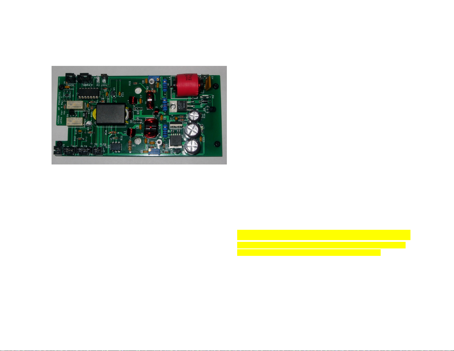
Section Two – Amplifier Module Construction
Circuit Board ID is HFPA-2013 V 4 R5
Circuit Board Assembly, HFPA V5
Assembly Steps
•Install 0.1 uF capacitors (104): C22, C4, C1, C9, C2,
C6, C8, C3, C7, C23 Install
•Install 47 pF (470J): C5
•Install 0.01 uF capacitors (103): C11, C10, C12
•Install 1000 pF capacitor (102): C13 Install
•Install 1 uF capacitor (105): C17. The long lead is (+)
and goes in square pad marked (+)
•Insert 1N4007 diode at D2 (smaller of two axial
components with cathode stripe at one end). Bend
leads very close to the body to match the component
outline on the board. Make sure cathode bar on the
part matches the cathode symbol on the silk screen
outline.Install
•Insert RL251 diode at D5. The leads are bent
approximately 1/8 inch away from the body to fit the
component outline on the board. Make sure cathode
bar on the part matches the cathode symbol on the silk
screen outline. Install
•Install six 1K 1/8W resistors (BRN BLK RED): R14,
R20, R15, R10, R21 and R12. Install
•Insert two 4.7K 1/8W resistors (YEL VIO RED): R17,
R19. Install
•Insert two 27 ohm ½ w resistors (RED VIO BLK):
R1,R2 Install
•Insert three 10K 1/8w resistor (BRN BLK ORN): R5,R6
and R4 Install (R5 partial symbol on board)
•Insert one 27K 1/8w resistor (RED VIO ORN): R13.
Install
•Insert one 3K 1/4W resistor (ORN BLK RED): R18.
Install
•Insert two 1.2K 1/8W resistor (BRN RED RED): R16,
R22. Install
•Insert one 1M 1/8w resistor (BRN BLK GRN): R11
Install
Note: if you did not purchase the PINET 100-PI Option Module,
install R3, R7 and R8 next. Otherwise wait until instructed to install
alternate values for R3, R7 and R8 in the 100-PI section.
•Insert two 100 ohm 2W resistors at R7 and R8. Install
•Insert one 62 ohm 2W resistor at R3. Install

•Insert one 78L05 regulator (3 pin TO92 package) at
U1. Match the outline.
•Insert four 2N5089 transistors (3 pin TO92 package) at
Q3, Q4, Q5, Q6 Match the outline. Install
•Insert two 2-pin headers (no rib back) at H3, H4. Install
•Insert Diode D3, 1N4148 at the D3 location. Install
•Insert three 2-pin headers at J1, J3, J6. Install
•Insert one 3-pin header at J4. Install
•Insert two 4-pin headers at J2 and J5. Install
•Insert two Power Tabs at H1 and H2. Solder one pin,
reheat and align perpendicular. Solder both pins of
each tab Install
•Insert one Circuit breaker, CB1. Leave leads long.
Insert just the tips through the board. Install
•Insert Inductor (Red 50 uh coil) at L4. Note that L4
leads are adjusted to fit the hole pattern. The ends are
not symmetrical. Install the bent lead to the right as
shown. Press the component flat on the circuit board.
Solder the pins, flush cut and re-solder the
connections. Install
•Insert two 10K- potentiometers, VR1 and VR2, on the
board. The lead under the adjustment screw is inserted
in the square pad in the circuit outline. Do not bend the
leads. Solder one pin, reheat and align part
perpendicular and flat on the board. Solder all pins
Install
•Turn the 25-turn potentiometers CCW at least 20 turns.
You will not hear a click and there is no mechanical
stop.
•Install the 14 pin DIP socket for U2. Align the notch on
the socket with the notch shown on the component
outline. Solder one corner pin. Reflow connection while
pressing the socket flat. Solder the other corner pin.
Reflow the pin while pressing the socket flush. Solder
the remaining pins. Install
•Insert U2, PIC16F688 Integrated Circuit in the socket
Install
•Insert two relays at K2, K3. Do not bend or cut the
leads. Solder one corner pin. Reflow while pressing the
relay flat to the board. Solder the other corner pin.
Reheat pin as necessary to make the relay flat to the
board. Solder all pins Install
•Insert two 330 uF Capacitor at C21 and C16. The long
lead (+) goes to the square pad of outline near the (+)
symbol on the board. Solder one pin, reflow and align
part flush. Solder other pin repeating reflow and
alignment. Flush cut leads and reflow. Install
•Insert one 100 uF Capacitor at C15. The long lead (+)
goes to the square pad of outline near the (+) symbol
on the board. Solder one pin, reflow and align part
flush. Solder other pin repeating reflow and alignment.
Flush cut leads and reflow. Install
•Insert a MBR1060G diode (2 pin package) in the
outline for D4. The part is mounted vertically. Press the
part down until the body is resting on the circuit board.
Install
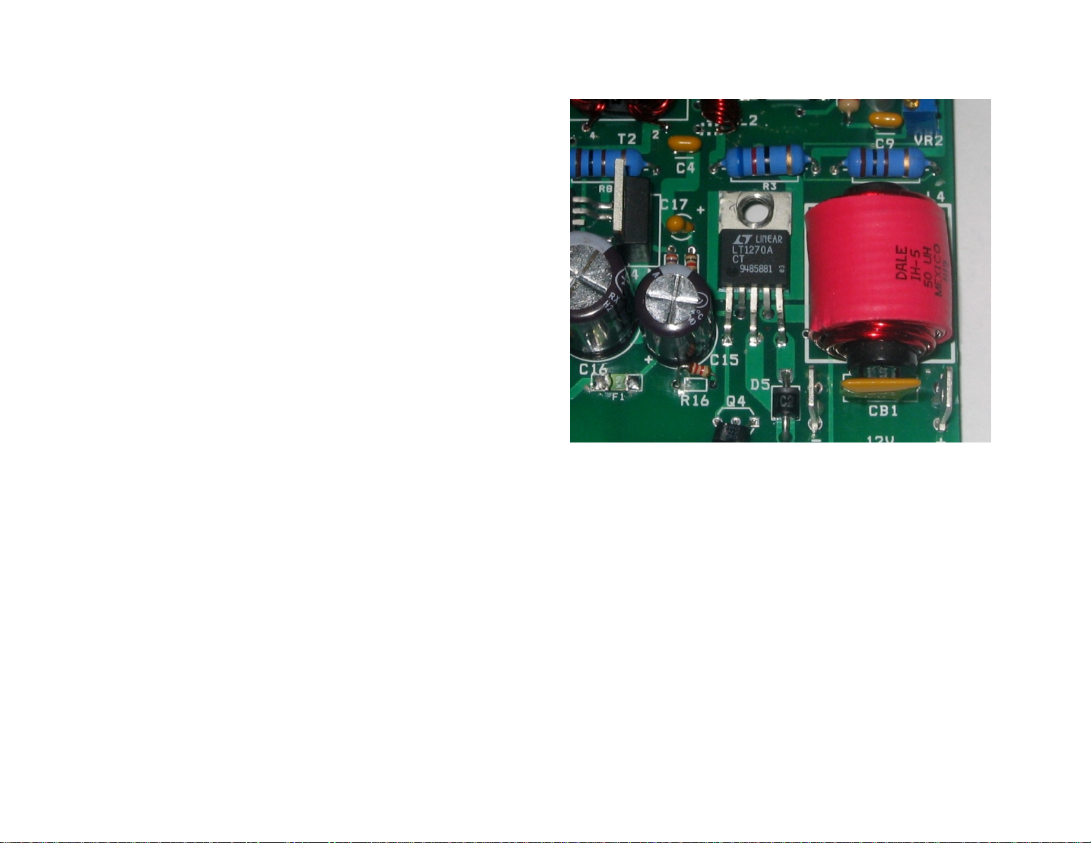
•Insert a LT1270A Switching Regulator U4 is mounted
horizontal into the 5 holes on the circuit board outline
for U4. First bend the legs straight. Bend to match
pattern while keeping the mounting hole centered. You
will later screw this component down to a stud
projecting from the heat sink below.
LT1270ACT Lead Insertion Detail
•Install 4N33, 6-pin IC at U3. Make sure the round
depression dot on the package is closest to the notch
in the component outline. Install
Spacer Assembly
•Locate four 4-40 x ¼ inch threaded hex spacers and
four 4-40 x 3/16 inch length screws.
•Install the spacers on the bottom side of the circuit
board. Tighten the screws extra snug so they will not

come loose when removing the circuit board from the
case in the future.
•Locate two 4-40 x ¾ inch threaded round spacer and
two 4-40 x ¼ inch length screws.
•Install the spacers on the top side of the circuit board
near VR1 and VR2. Tighten the screws extra snug so
they will not come loose when removing the filter
module in the future.
Note: Identify the correct size wire for T2 and T3
Fabrication and Assembly of T2
•Two stacked FT50-43 torroid cores are used for this
transformer. Cut two #22 AWG wire (0.026 inch diameter)
15 inches long. Do not twist the wires. To prevent chaffing
of the wire on the edge of ceramic cores, insert a common
soda straw (same length as the thickness of the two
stacked cores). Through the stacked cores, insert the two
parallel wires. Bend the wires into a U-shape. Holding the
two wires together in one hand with the cores at the bottom
of the U-Shape, grasp the wires in the rear and insert the
wires on front right side through the core four additional
times. Pull each wrap snug keeping the wires parallel
without crossovers. After completion of the loops on the
right side, pass the remaining wires through the cores on
the front left side 5 times. Pull each wrap snug keeping the
wires parallel without crossovers. You will now have 10
turns passing through the core.
•Separate and scrape the ends of the wires so you can
measure continuity and isolation to determine the start and
finish of each wire.
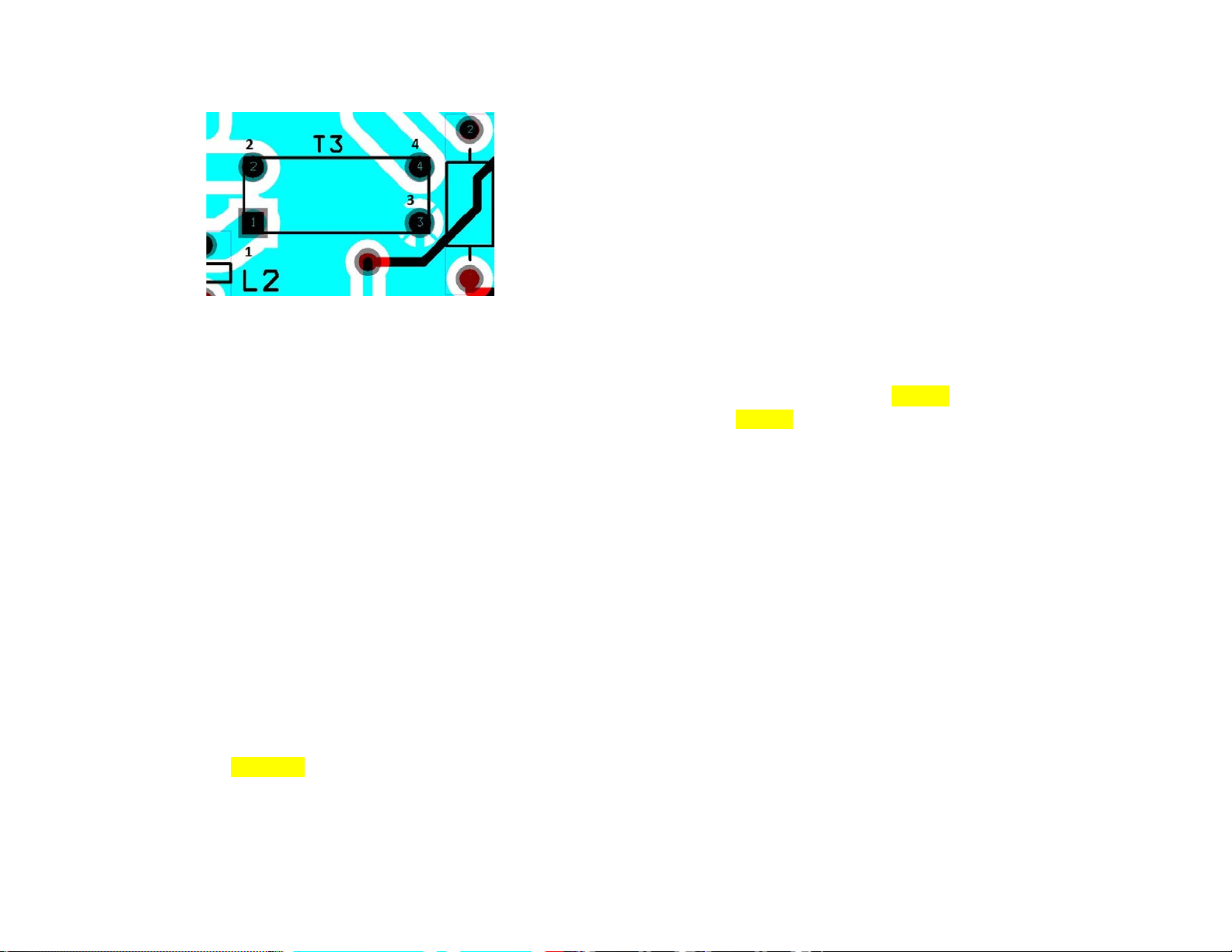
Circuit board showing cores with wire exits for T2 and T3
•Winding # 1 goes to pins 1 and 2. Winding #2 goes to
pins 3 and 4.
•Insert the wires through the appropriate holes and pull
snug to form the leads in the shape required.
•Remove T2 from the mounting holes and use a
soldering iron to heat the insulation at the points where
you will be soldering to the board. You need at least
750 degrees F to remove the insulation. Tin the leads
removing insulation and excess solder.
•Re-insert T2 on the board at the T2 outline. Pull the
leads tight and solder in place. Install
•Trim the excess lead length and reflow connections.
•This is a typical spot where you can have a poor solder
connection. Inspect and re-solder if necessary.
Adjust the wire spacing to match the picture. The top and
bottom of the core should be clear so T2 and T3 will be
minimum height to not create a clearance problem with the
board above.
Fabrication and Assembly of T3
•One FT50-43 torroid core is used for this transformer.
Cut two #24 AWG wire (0.022 inch diameter) 11 inches
long . No twist is required or desired. Insert the two
wires through the core. Bend the wires into a U-shape.
Holding the two wires together in one hand with the
cores at the bottom of the U-Shape, grasp the wire in
the rear and insert the wires on the front right side
through the core four additional times. Pull each wrap
snug. Avoid crossover of the leads.
•After completion of the loops on the right side, pass
the remaining wires through the core on the front left
side 5 times. Pull each wrap snug. You will now have
10 turns passing through the core.
•Separate and scrape the ends of the wires so you can
determine the start and finish of each wire. Use the
multi-meter to measure continuity.
•Winding # 1 goes to pins 1 and 2. Winding #2 goes to
pins 3 and 4.
•Insert the wires through the appropriate holes and pull
snug to form the leads in the shape required.
•Pull T3 from the mounting holes and use a soldering
iron to heat the insulation at the points where you will
be soldering to the board. You need at least 750
degrees F to remove the insulation. Tin the leads
removing excess accumulated Install
•Re-insert T3 on the board at the T3 outline. Pull the
leads tight and solder. Install
•Trim the excess lead length and reflow connections.
Fabrication and Assembly of L1 and L3
•L1 and L3 are identical and require 12 inches each of
the remaining #24AWG wire.

•Use a ¼ inch drill bit as a winding form and wrap 10
complete turns of the wire tightly around the drill bit.
•Trim the excess lead length to ½ inch and tin the leads.
•Insert L1 and L3 into the L1 and L3 positions on the
circuit board. Install
•Use the end of a ball point pen to push into the end of
the air coils slightly to reform the wires should they
become deformed during soldering.
Fabrication and Assembly of L2
Note: If you purchased the PINET 100-PI Module with
your Amp, it is not necessary to install L2. Leave the holes
clear. Instead, refer to the page for the PINET 100-PI Module
option.
•L2 require 4 inches of the #24AWG remaining wire.
•Use a 3/16 inch drill bit as a winding form and wrap 4
complete turns of the wire tightly around the drill bit.
•Trim the excess lead length to ½ inch and tin the leads.
•Insert L2 into the L2 position on the circuit board. Install
•Use the end of a ball point pen to push into the end of
the air coils slightly to reform the wires should they
become deformed during soldering.
Assembly of RFM2
•Insert the RFM-2 Module in the U6 location.
•The square pad (pin 1) on PCB aligns with the square
pad on the RFM-2 Module. (see bottom right in pix
below)
RFM-2 just below U2 above
•T1 is fabricated using a Binocular core with a primary
and secondary winding.
•The primary is a 7 inch yellow #20AWG Teflon coated
wire. There will be 2 loops through the cores.
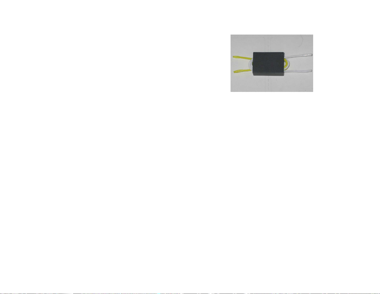
•The secondary is a 10 inch white #20 AWG Teflon
coated wire. There will be 3 loops through the cores.
•Make a U shape of the 7 inch yellow wire and insert
into the two tubes. Equal distance the wires.
•Make a U shape of the 10 inch white wire and insert
into the same end of the two tubes. Equal distance the
wires. At this point, you have 2 yellow and two white
wires coming out the same end.
•Push one of the yellow wire leads through the adjacent
tube. Push the other yellow wire lead through the other
adjacent tube. Pull the leads tight. You are finished
with the yellow wire.
•Push the white wires through in the same manner. Pull
the wires tight. Push the white wires through a final
time through the adjacent tubes. You now have the
yellow wire leads on one end and the white wire leads
on the other.
•You are done winding the core.
•Trim about 3/8 inch length off each lead. Strip each
wire about 3/8 inch and lightly tin the tip. You are now
ready to install the transformer into the board. The
yellow primary (input) and white secondary (output).
•Insert the primary wires at holes 1 and 2. Pin 1 is the
square pad.
•Insert the secondary into holes 3 and 4
•Pull leads snug and solder. Install
T1 with Yellow Primary, White Secondary
Clean and Inspect the Board
•Remove the flux from the circuit board with a flux
removal spray in a ventilated space.
•Inspect the solder joints for the entire board
This completes assembly of this module. The MOSFETs will
be installed in a later assembly.
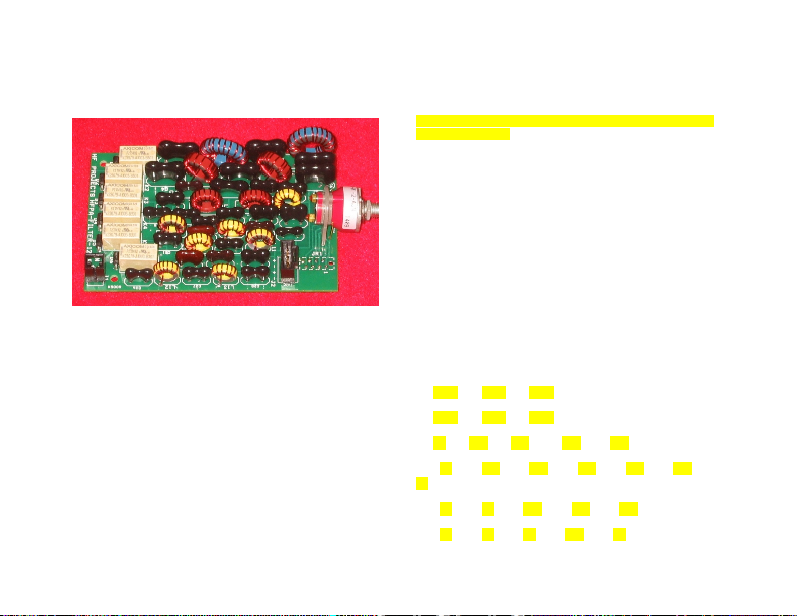
Section 3 - Low Pass Filter Module Assembly
This is the 10‐Band Filter Module HFPA‐FILTER‐12
Size: 3.8 x 2.4 inch; Bands: 160‐10M Power Rating: 50W; Control:
Front panel switch
Design: Four‐Layer Ground Plane with greater than ‐40dB
rejection in the stop band;
Relay Front End controlled by front panel switch, LED display.
Organize for Assembly
Place on the table in front of you all the capacitors ranging
from smallest value to largest value from left to right.
Organize the cores and relays into like groups.
Two Blue Cores – T68-1
Two Larger Red Cores – T50-2
Two Smaller Red Cores – T44-2
Seven Yellow Small Cores – T37-6
Wind the cores referring to the core winding table
"REALLY CHECK THE POLARITY OF THE DIODES FOR THE RELAYS
ON THE LPF BOARD"
Install Relays and Diodes
Install the six diodes on the circuit board observing that the
stripe on the diode matches the board silkscreen for the part.
Be careful that your tools do not damage the circuit board. The
diodes require that the leads are bent very close to the body of
the diode. Before installing, scrape the leads near the body to
remove any oxidation on the leads. Install
Install six relays. Solder one pin, reheat and align flat. Install
Capacitor Assembly
Install the capacitors in the sequence given and soldering
when called for. The part may be oversized for the insertion
holes. Form the leads for a best fit. Double check your work.
C1 1500, C2 2700, C3 1500 Install
C4 1000, C5 1800, C6 1000 Install
C7 39, C8 110, C9 390, C10, 680, C11 330 Install
C12 27, C13 150, C14 100, C15 100, C16 220, C17 220, C18
47 Install
C19 12, C20 39, C21 150, C22 220, C23 100 Install
C24 12, C25 39, C26 82, C27 150, C28 68 Install

Core Winding Table
REF
TYPE
T
IN.
Wire
IND.
Clock
L1, L2
T68-1
(BLU)
20
19
22
5.08 uH
7-5
L3,L4
T50-2
(RED)
22
17
24
2.65 uH
7-5
L5
T44-2
(RED)
15
13
24
1.37 uH
7-5
L6
T44-2
(RED)
13
12
24
1.17 uH
7-5
L7
T37-6
(YEL)
12
9
24
580 nH
7-5
L8
T37-6
(YEL)
11
8
24
470 nH
5-7
L9
T37-6
(YEL)
10
8
24
430 nH
8-3
L10
T37-6
(YEL)
11
8
24
470 nH
7-5
L11
T37-6
(YEL)
10
8
24
430 nH
7-5
L12
T37-6
(YEL)
8
7
24
360 nH
10-2
L13
T37-6
(YEL)
7
7
24
280 nH
11-1
Where: T=turns; IN.=inches; IND= inductance; Wire=AWG
Clock – Clock Face where winding occupy space on the
core between a start time (7pm) and a end time (5pm)
example. Evenly adjust the wire spacing to match the clock
setting.
Core Winding Technique
The starting position: Divide
the wire in half letting the
core hang down. The wire
passing through the core
counts as one turn.
L3 Example:
Wind one side. Start with
the wire in the back and
wrap 10 turns on the right
side.
Use a pair of needle nose
pliers to aid in pulling
the wire tight against the
core as you wrap it around
the core.
Wind the other side. Wrap
10 turns on the other
side.You now have 21 turns
through the core. I
squeeze up the wraps to be
tight. Your inductors must
be wound with the wires on
the sides shown or the
inductor footprint will
not match the circuit board layout.
If the core does not fit the pattern (wound wrong), do not
try to make it work, strip the wire and wind it again correctly.
Spread the windings equally about the core using the clock
code.
Core Installation
Install L1-L2 last because of the size (see picture for detail).
Install L3-L13. Pull the leads tight. Align the core vertical
and solder.
Repeat for each inductor one by one. Solder as you go.
Install
Switch Assembly
Insert the switch on the top side of the assembly. Make sure
the leads are flush with the board. Install
Connector Assembly
Insert J1 and J2. Make sure the parts are flush and vertical.
Solder one pin to start, reheat while making final alignment.
Solder the remaining pins. Make sure the friction tab is in the
position shown below. The J1 tab is to the right and the J2 tab
is down in the drawing below. Install
Insert JR1. This component is installed from the back side of
the circuit board and soldered on the top side. It will only fit the
pattern one way. See picture below. Solder. Install

In-Circuit Tuning Adjustments
If you have a miniVNA device for your PC you can adjust the
filter in real-time for the best response curve. If you do not, you
can use the clock method of lead spacing and you should be
pretty close.
Note: You must attach 12V to J2 in order to use a
miniVNA. Observe polarity, pin 1 is +12V. You need power
because only the energized circuit does not have the input and
outputs grounded.
Consolidated Filter Response Where Y-axis = dB; X-axis = F
MHz
The Plot was acquired using a miniVNA sweeping 1 – 100
MHz. Data was captured to an Excel spread sheet and
graphed.
Selector Switch Stop Pins Installation
•The switch includes a little package that has two stop
pins and a sticker. Your goal is to install the pins in the
correct holes without losing the stop pins.
•Turn the shaft so the flat is on the right. Check ___
•Insert the pins at 12 and 6 o’clock. Cover with sticker.
Install
‐60
‐50
‐40
‐30
‐20
‐10
0
10
050 100 150 F160 dB
F8075 dB
F6040 dB
F3020 dB
F1715 dB
F1210 dB
Table of contents
Popular Amplifier manuals by other brands

AMS
AMS 1073DPA user guide

DX Engineering
DX Engineering RF-KIT Operating and Installing Instructions

Harris
Harris DA-DHR6804+D Installation and operation manual

Dekolink
Dekolink MW-CBDA-SMR-800-900-1W65 Installation and operating instructions

Kistler
Kistler 5074A Series instruction manual

Adcom
Adcom GFA-5800 Service manual


Ashly
Ashly Electronic Amplifier none operating instructions

Cobalt Digital Inc
Cobalt Digital Inc 9910-DA-AV product manual

Crown
Crown PSA-2 Specifications

Origin Effects
Origin Effects Cali76 instructions

Navison audio
Navison audio NVS-003G Setup and operation manual

FiberLabs
FiberLabs EDFA-1550 Series Technical Passport