CPCB48MIO0001A Interface Card
2
CPCB48MIO0001A Interface Card
This interface card is used in conjunction with the CICE48C00CCF
U 1
U 2
U 3
U 5
U 6
U 7 U 8
U 9
U 4
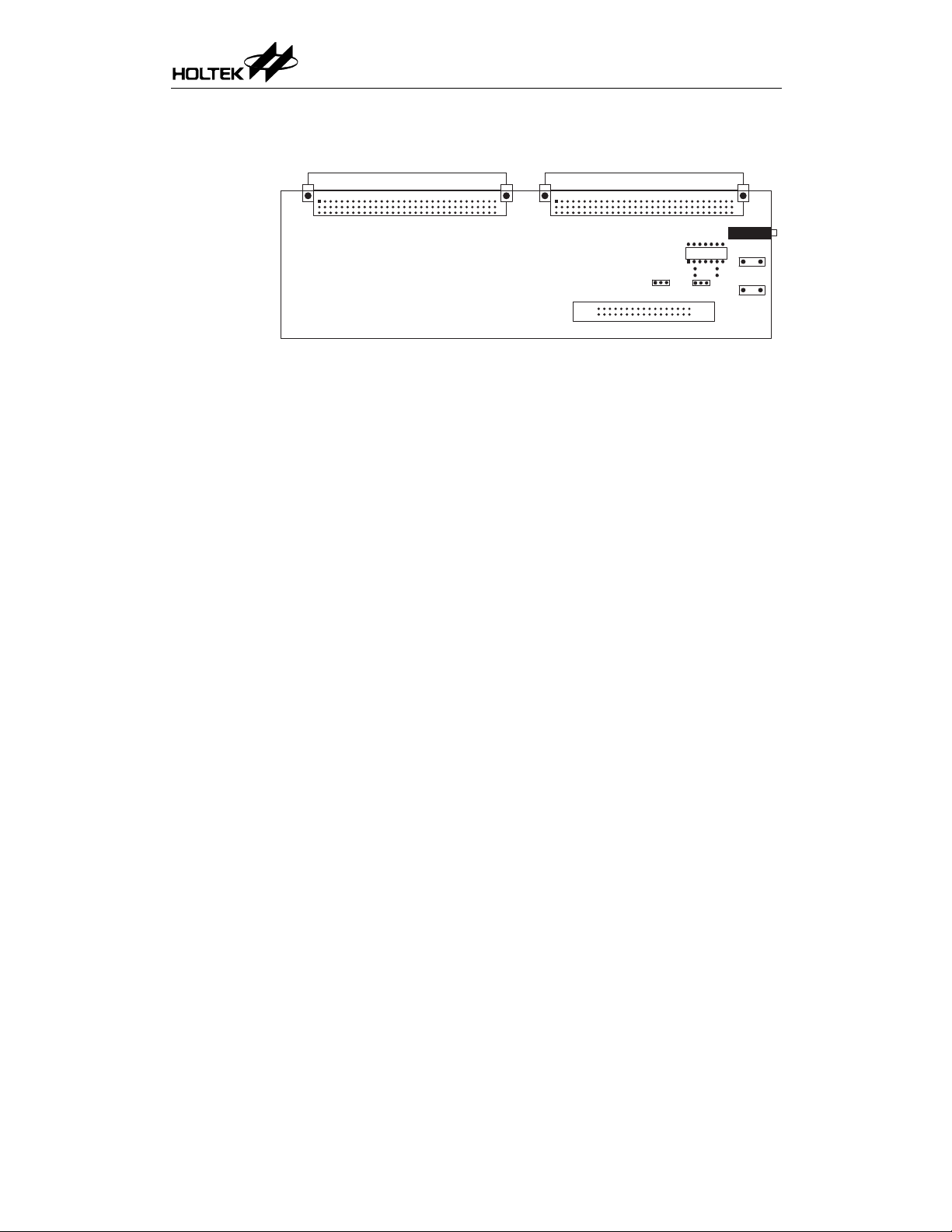
J P 1
S W 1
J P 4
J P 3
V R 1
S W 2
Y 1
The external clock source has two modes, RC and Crystal. If a crystal clock is to be
used, positions 2 and 3 should be shorted on JP4 and a suitable crystal inserted into
location Y1. Otherwise, if an RC clock is to be used, positions 1 and 2 should be
shorted and the system frequency adjusted using VR1. Refer to the Tools/Mask
Option menu of the HT-IDE3000 User′s Guide for the clock source and system
frequency selection.
The four external signal trace inputs, marked as ET0 to ET3 at jumper location JP3,
provide a means for external signals to trigger the internal breakpoint and trace
functions. For more information, refer to the chapters on Breakpoint and Trace the
Application Program within the Holtek HT-IDE3000 User′s Guide.
The JP1 connector provides the I/O port connections as well as other pins. The DIP
switch, SW1, should be set according to which device is selected and in accordance
with the following table:
SW1 1 2 3 4 5 6 7
HT48X10 OFF OFF ON OFF ON OFF OFF
HT48X05-18 OFF OFF ON OFF ON OFF OFF
HT48X06-18 OFF OFF ON OFF ON OFF OFF
HT48X3X ON OFF OFF ON OFF OFF ON
HT48X5X-28 ON OFF OFF ON OFF OFF ON
HT48X5X-40 ON OFF OFF OFF OFF OFF OFF
HT48X7X-40 OFF OFF OFF OFF OFF OFF OFF
HT48XA0-24 OFF OFF OFF OFF OFF OFF OFF
HT48XA6-24 OFF OFF OFF OFF OFF OFF OFF
HT48X37-24 OFF ON OFF OFF OFF ON OFF
Switch SW2 controls the carrier output of the HT48CA6 device. When in the up
position, the PC0 pin is the carrier output. For all other MCU types or if PC0 is not
used as a carrier output, the switch should be set in the down position.
SW2 MODE
↑
HT48CA6 CARRIER OUTPUT
↓
OTHERS