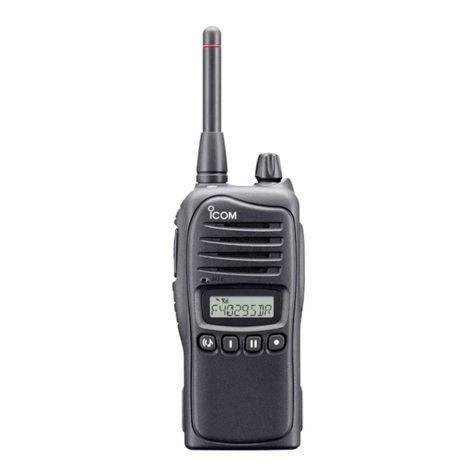
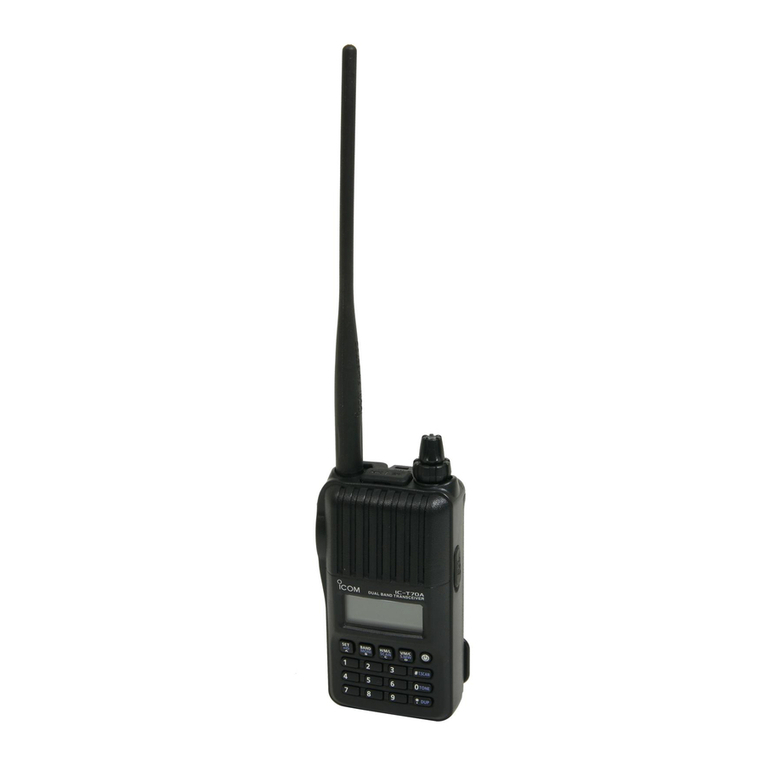
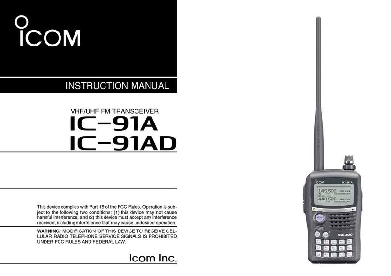
Icom IC-E7 User manual

SERVICE
MANUAL
VHF/UHF DUALBAND FM TRANSCEIVER
S-14217HZ-C1
Nov. 2005

INTRODUCTION
This service manual describes the latest service information
for the IC-E7 VHF/UHF DUALBAND FM TRANSCEIVER at
the time of publication.
ORDERING PARTS
Be sure to include the following four points when ordering
replacement parts:
1. 10-digit Icom parts number
2. Component name and informations
3. Equipment model name and unit name
4. Quantity required
<SAMPLE ORDER>
5030002860 LCD A01B004X IC-E7 Main unit 5 pieces
8810008990 Screw PH B0 2×10 ZK IC-E7 Chassis 10 pieces
Addresses are provided on the inside back cover for your
convenience.
REPAIR NOTES
1. Make sure the problem is internal before disassembling the transceiver.
2. DO NOT open the transceiver until the transceiver is disconnected from its power source.
3. DO NOT force any of the variable components. Turn them slowly and smoothly.
4. DO NOT short any circuits or electronic parts. An insulated turning tool MUST be used for all adjustments.
5. DO NOT keep power ON for a long time when the transceiver is defective.
6. DO NOT transmit power into a signal generator or a sweep generator.
7. ALWAYS connect a 30 dB to 40 dB attenuator between the transceiver and a deviation meter or spectrum analyzer when
using such test equipment.
8. READ the instructions of test equipment thoroughly before connecting equipment to the transceiver.
To upgrade quality, all electrical or mechanical parts and internal
circuits are subject to change without notice or obligation.
MODEL VERSION SYMBOL
IC-E7
Europe EUR
Italy ITR
France FRA
United Kingdom UK
Icom, Icom Inc. and logo are registered trademarks of Icom Incorporated (Japan) in the United States, the United
Kingdom, Germany, France, Spain, Russia and/or other countries.
NEVER connect the transceiver to an AC outlet or to a DC
power supply 3.7 V. Such a connection could cause a fire or
electric hazard.
DO NOT expose the transceiver to rain, snow or any liquids.
DO NOT reverse the polarities of the power supply when
connecting the transceiver.
DO NOT apply an RF signal of more than 20 dBm (100 mW)
to the antenna connector. This could damage the trans-
ceiver's front end.
DANGER

TABLE OF CONTENTS
SECTION 1 SPECIFICATIONS
SECTION 2 INSIDE VIEWS
SECTION 3 DISASSEMBLY INSTRUCTIONS
SECTION 4 CIRCUIT DESCRIPITON
4 - 1 RECEIVER CIRCUITS . . . . . . . . . . . . . . . . . . . . . . . . . . . . . . . . . . . . . . . . . . . . . . . . . . . . . . . . . . . . . . 4 - 1
4 - 2 TRANSMITTER CIRCUITS . . . . . . . . . . . . . . . . . . . . . . . . . . . . . . . . . . . . . . . . . . . . . . . . . . . . . . . . . . . 4 - 2
4 - 3 PLL CIRCUITS . . . . . . . . . . . . . . . . . . . . . . . . . . . . . . . . . . . . . . . . . . . . . . . . . . . . . . . . . . . . . . . . . . . . 4 - 3
4 - 4 PORT ALLOCATIONS . . . . . . . . . . . . . . . . . . . . . . . . . . . . . . . . . . . . . . . . . . . . . . . . . . . . . . . . . . . . . . . 4 - 4
4 - 5 POWER SUPPLY CIRCUITS. . . . . . . . . . . . . . . . . . . . . . . . . . . . . . . . . . . . . . . . . . . . . . . . . . . . . . . . . . 4 - 5
SECTION 5 ADJUSTMENT PROCEDURES
5 - 1 PREPARATION . . . . . . . . . . . . . . . . . . . . . . . . . . . . . . . . . . . . . . . . . . . . . . . . . . . . . . . . . . . . . . . . . . . . 5 - 1
5 - 2 FREQENCY AND TRANSMIT ADJUSTMENT . . . . . . . . . . . . . . . . . . . . . . . . . . . . . . . . . . . . . . . . . . . . .5 - 4
5 - 3 RECEIVE ADJUSTMENT . . . . . . . . . . . . . . . . . . . . . . . . . . . . . . . . . . . . . . . . . . . . . . . . . . . . . . . . . . . . 5 - 5
SECTION 6 PARTS LIST
SECTION 7 MECHANICAL PARTS AND DISASSEMBLY
SECTION 8 SEMICONDUCTOR INFORMATION
SECTION 9 BOARD LAYOUTS
9 - 1 MAIN UNIT . . . . . . . . . . . . . . . . . . . . . . . . . . . . . . . . . . . . . . . . . . . . . . . . . . . . . . . . . . . . . . . . . . . . . . . 9 - 1
9 - 2 PA BOARD. . . . . . . . . . . . . . . . . . . . . . . . . . . . . . . . . . . . . . . . . . . . . . . . . . . . . . . . . . . . . . . . . . . . . . . . 9 - 1
9 - 3 VCO BOARD . . . . . . . . . . . . . . . . . . . . . . . . . . . . . . . . . . . . . . . . . . . . . . . . . . . . . . . . . . . . . . . . . . . . . . 9 - 1
SECTION 10 BLOCK DIAGRAM
SECTION 11 CIRCUIT DIAGRAM
SECTION 12 BC-164

1 - 1
SECTION 1 SPECIFICATIONS
GENERAL
• Frequency range :
Version Transmit (MHz) Receive (MHz)
[EUR],
[UK]
144.000–146.000
430.000–440.000 0.495–999.990
[ITR]
144.000–146.000
430.000–434.000
435.000–438.000
144.000–146.000
430.000–434.000
435.000–438.000
[FRA] 146.000–146.000
430.000–440.000
0.495–29.995
50.200–51.200
76.000–135.995
144.000–146.000
430.000–440.000
• Operating mode : FM, AM*, WFM* (*RX only)
• Memory channels : 1000 channels
• Call channels : 2 channels
• Scan types : F ull/Program/Priority/
Memory Channel/Bank/
Bank-Link/Skip/Tone
• Frequency stability : ±6 ppm (–10°C to +60°C)
• Tuning steps : 5/6.25/8.33/9/10/12.5/15/20/
25/30/50/100 and 200 kHz
• Antenna impedance : 50 Ω(SMA type)
• Power supply requirement : Specified Icom's battery
pack only
(operating voltage 3.7 V)
• Current drain :
TRANSMIT VHF High 1.5 A
Low 0.4 A (approx.)
UHF High 1.5 A
Low 0.5 A (approx.)
RECEIVE Stand-by 80 mA (approx.)
Max. audio
Less than 150 mA
• Operating temp. range : –10°C to +60°C
• Dimensions
(projections not included)
:
47 (W) × 81 (H) × 28 (D) mm
• Weight
(antenna, BP-243 included)
: 160 g (approx.)
• MIC/SP connector : 4-conductor 3.5 (d) mm; (
1/8′′
)
2 kΩ/8 Ω
TRANSMITTER
• Output power :
VHF
UHF
1.5 W (High)
0.1 W (Low; aprrox.)
1.0 W (High)
0.1 W (Low; aprrox.)
• Modulation system : Variable reactance frequency
modulation
• Maximum deviation : ±5.0 kHz
• Spurious emissions : Less than –60 dB (TX High)
Less than –50 dB (TX Low)
RECEIVER
• Receiving system : Double conversion
superheterodyne system
• Intermediate frequencies :
FM, AM 1st; 46.35 MHz
2nd; 450 kHz
WFM 1st; 14.85 MHz
2nd; 450 kHz
• Sensitivity* :
(except spurious points; maximum sensitivity)
Frequency (MHz) FM AM WFM
0.495–4.995 –+7 dBµ
–5.000–29.995 +3 dBµ
30.000–75.995 –7 dBµ
–
76.000–89.995 +5 dBµ
90.000–107.995
–14 dBµ
108.000–117.995
–
118.000–136.995 +3 dBµ
137.000–143.995
–
144.000–147.995 –15 dBµ
148.000–179.995 –14 dBµ
330.000–369.995 +5 dBµ
370.000–399.995 –10 dBµ
400.000–429.995 –13 dBµ
430.000–449.995 –15 dBµ
450.000–499.995 –5 dBµ
600.000–799.990 0 dBµ +8 dBµ
799.995–939.990 –
940.000–999.990 +5 dBµ
*FM and WFM are measured at 12 dB SINAD, AM is easured
at 10 dB S/N.
• Squelch sensitivity
(at threshold)
: Less than –15 dBµ
• Selectivity :
FM, AM More than 12 kHz/6 dB
Less than 30 kHz/60 dB
WFM More than 150 kHz/10 dB
Less than 700 kHz/20 dB
• Spurious image rejection : More than 40 dB
• Audio output power : More than 50 mW at 10%
distortion with an 8 Ωload
All stated specifications are subject to change without notice or obligation.

SECTION 2 INSIDE VIEWS
2 - 1
CPU
CPU
(IC4: M30220FCRP)
(IC4: M30220FCRP)
PTT detector
PTT detector
(Q14: 2SA1832)
(Q14: 2SA1832)
D/A convertor
D/A convertor
(IC13: BH2220FVM)
(IC13: BH2220FVM)
Reference
Reference
frequency generator
frequency generator
(X1: CR-813 7.325MHz)
Reset IC
Reset IC
(IC2: R3112N291A)
(IC2: R3112N291A)
CPU
(IC4: M30220FCRP)
PTT detector
(Q14: 2SA1832)
D/A convertor
(IC13: BH2220FVM)
CTCSS filter
(IC5: LM2904PWR)
Microphone amplifier
(IC8: LMV324IPW)
Reference
frequency oscillator
(X1: CR-813 7.325 MHz)
Reset IC
(IC2: R3112N291A)
Antenna switch circuit
+3V regulator
+3V regulator
(IC10: R1111N321B)
(IC10: R1111N321B)
PLL IC
PLL IC
(IC18: ADF4110BCPZ)
(IC18: ADF4110BCPZ)
VCO board
VCO board
AF volume
AF volume
(IC7: SM6451B)
(IC7: SM6451B)
AF amplifier
AF amplifier
(IC9: NJM2070M)
(IC9: NJM2070M)
IF IC
IF IC
(IC15: TA31136FNG)
(IC15: TA31136FNG)
1st mixer
1st mixer
(IC16:
(IC16:
µPC2757TB)
PC2757TB)
Antenna switching circuit
+3V regulator
(IC10: R1111N321B)
PLL IC*
(IC18: ADF4110BCPZ)
VCO board
* Located under the VCO board
AF volume*
(IC7: SM6451B)
AF power amplifier
(IC9: NJM2070M)
FM IF IC
(IC15: TA31136FNG)
1st mixer
(IC16: µPC2757TB)
• MAIN UNIT (TOP VIEW)
• MAIN UNIT (BOTTOM VIEW)
• PA BOARD
Final amplifier*
Final amplifier*
(Q3: RQA003)
(Q3: RQA003)
Drive amplifier
Drive amplifier
(Q2: 2SC5998)
(Q2: 2SC5998)
Pre drive amplifier
Pre drive amplifier
(Q1: 2SC5006)
(Q1: 2SC5006)
Power amplifier*
(Q3: RQA003)
Drive amplifier
(Q2: 2SC5998)
Pre-drive amplifier
(Q1: 2SC5006)
* Located bottom side of the point.

SECTION 3 DISASSEMBLY INSTRUCTIONS
3 - 1
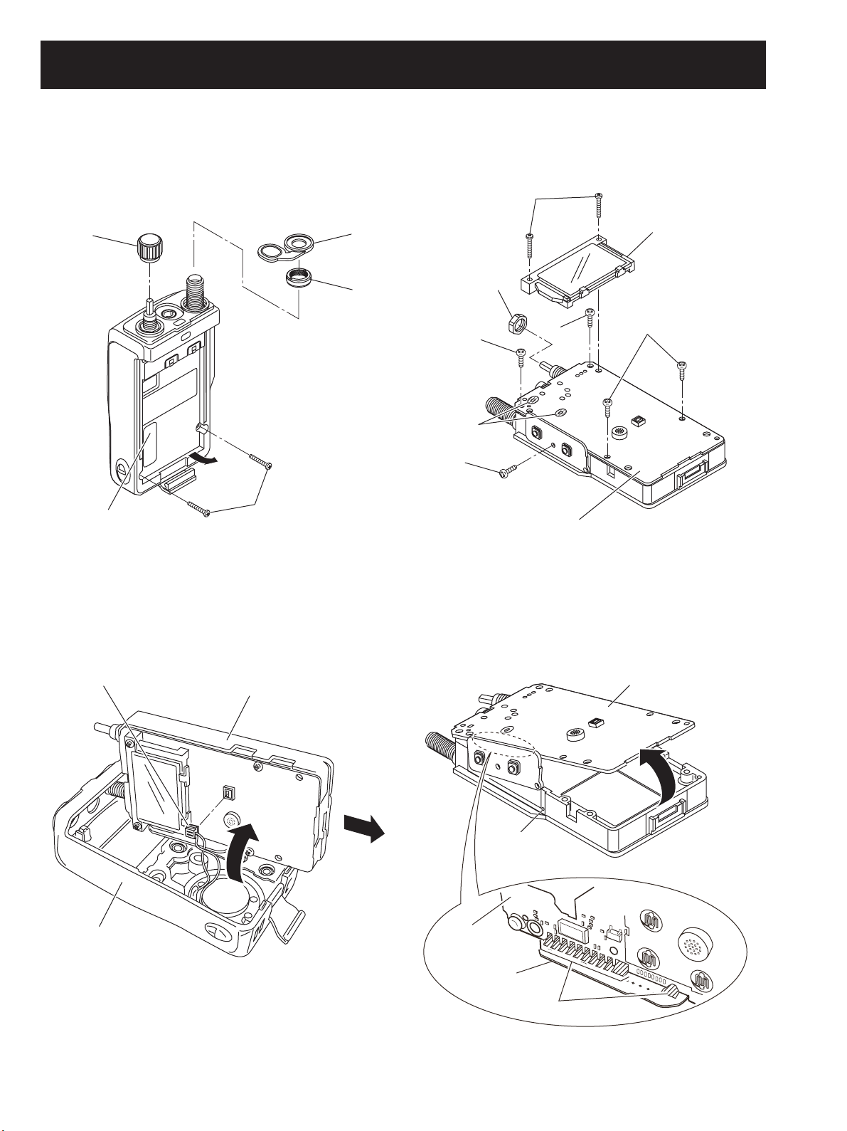
• Removing the chassis
1Remove the battery pack.
2Remove the jack cap Aand unscrew the antenna nut B.
3Remove the dial knob C.
4Unscrew 2 screws Dand lift up the chassis in the direction
of the arrow.
• Removing the MAIN unit and PA board
1Unscrew 2 screws A, then remove the LCD panel B.
2Unscrew 5 screws Cand dial nut D.
3Unsolder 2 points E.
5Incline the chassis as figure below and disconnect the
speaker cable E.
6Remove the chassis from the front panel.
Chassis
A
B
C
D
Chassis
Front panel
E
MAIN unit
B
C
E
CC
D
A
C
4Release the projection F, and remove the MAIN unit.
5Unsolder 11 points Gand remove the PA board from the
MAIN unit.
MAIN unit
F
PA board
G
MAIN unit
(Top side)

SECTION 4CIRCUIT DESCRIPTION
4-1 RECEIVE CIRCUITS
4-1-1RF CIRCUITS (MAIN UNIT)
This transceiver has 4 RF circuits to provide wide receiving
range. The received signals from the antenna connector
(CHASSIS; J1) are applied to each RF circuits for the frequency
coverage, and amplified within the frequency coverage.
• While receiving 0.495–76 MHz
The 0.495–76 MHz band signals are passed through the
three low-pass filters (LPF; L32, L34, L39, L42, C284, C290,
C294, C307, C314), then applied to the RF amplifier (Q38)
via the band switches (D30, D43) and LPF or BPF.
The 0.495–30 MHz band signals are passed through the
LPF (L20, C241, C242, C247), the 30–76 MHz signals are
passed through the Bandpass Filter (BPF; D39, L21, L24,
C238, C256) before being applied to the RF amplifier (Q38).
The amplified signals are applied to the 1st mixer (IC16, pin
1) via the band switch (D16).
- 0.495–76 MHz -
• While receiving 76–300 MHz
The 76–300 MHz band signals are passed through two LPFs
(L39, L42, C307, C314) and a couple of High-pass Filter (HPF;
L33, C287, C293) and LPF (L29, L31, C266, C269, C276,
C283, C514, C516), then applied to the RF amplifier (Q42) via
the antenna switching circuit (D35, D38) and the LPF (D53,
L44, C295, C303).
The amplified signals are then applied to the 1st mixer (IC16, pin
1) via the BPF (D27, D28, D31, D36, L10, L11, L22, L23, C208,
C210, C216, C228, C233, C243) and band switch (D21).
- 76–300 MHz -
4 - 1
ST)&SIGNAL
TOTHE&-)&)#
)#PIN -(Z
7&-
$ &)
&)
1
$
-(Z
!-&-
2ECEIVEDSIGNALS
FROMTHE2&CIRCUITS
SIGNALS
FROMTHE6#/S
ST)&
"0&
"0&
STMIXER
)#
to the
1st mixer
(IC16, pin 1)
0.495–30 MHz
D39
D16
D30
Q38 D43 D44
30–76 MHz
from the
antenna
RF
amp
LPF
AT T
BPF
LPF
LPF
3 LPF’s
to the
1st mixer
(IC16, pin 1)
D21
D53
D27, D28,
D31, D36 Q42
from the
antenna
BPF LPF
LPF
LPF
HPF
LPF
RF
amp
2 LPF’s
D35, D38
ANT
SW
• While receiving 300–500 MHz
The 300–500 MHz band signals are passed through the LPF
(L42, C314) and a couple of HPF (L38, C302, C306) and
LPF (D41, D45, L26, L30, C255, C257, C262, C275, C282,
C289, C515), then applied to the RF amplifier (Q43) via the
antenna switching circuit (D34, D37) and the BPF (D55, L36,
L106, C304, C522, C523).
The amplified signals are then applied to the 1st mixer
(IC16, pin 1) via the BPF (D26, D32, L13, L25, C204, C215,
C222, C236, C244, C520, C521) and band switch (D22).
- 300–500 MHz -
to the
1st mixer
(IC16, pin 1)
D55 D41, D45D26, D32
D22 Q43
LPF
BPFBPF HPF
LPF from the
antenna
RF
amp
D34, D37
ANT
SW
• While receiving 500–999 MHz
The 500–999 MHz band signals are passed through the HPF
(L41, C311, C313) and band switch (D54), then applied to
the RF amplifier (Q45) via the attenuator (D46). The amplified
RF signals are applied to another RF amplifier (Q39) via the
BPF (D33, D40, L15, L27, L28, C229, C237, C245, C252,
C261). The amplified RF signals are then applied to the 1st
mixer (IC16, pin 1) via the band switch (D23).
- 500–999 MHz -
to the
1st mixer
(IC16, pin 1)
D23 Q39 Q45 D54
D46
AT T from the
antenna
HPF
BPF
RF
amp RF
amp
D33, D40
4-1-2 1ST IF CIRCUITS (MAIN UNIT)
The 1st IF circuits contain the 1st mixer, 1st IF amplifier
and the 1st IF filter. The 1st IF mixer converts the received
signals into a fixed frequency of the 1st Intermediate
Frequency (IF) signal. The converted 1st IF signal is filtered
at the 1st IF filters, then amplified at the 1st IF amplifier.
The received signals from the RF circuits are applied to the
1st IF mixer (IC16, pin 1), and converted into the 46.35 MHz
(AM/FM)/14.85 MHz (WFM) 1st IF signal by being mixed
with 1st Local Oscillator (LO) signals from the VCOs (VCO
BOARD).
While receiving 0.5–76 MHz band signals, the 1st LO signals
are generated at 50 MHz VCO (VCO BOARD; Q10, Q13,
D7, D8), and for receiving 76–280 MHz band signals, the 1st
LO signals are generated at 144 MHz VCO (VCO BOARD;
Q9, Q12, D6).
While receiving 280–999 MHz band signals, the 1st LO
signals are generated at 430 MHz VCO (VCO BOARD; Q8,
Q11, D5). If the receiving frequency is 500 MHz and above,
the VCO output signal is doubled at the doubler circuit (Q18)
before being to applied to the 1st mixer (IC16, pin 3).
The converted IF signal is passed through the 1st IF filter
FI3 (AM/FM mode) or FI2 (WFM mode) to filter out the
unwanted signal, then applied to the 1st IF amplifier (Q9).
The amplified 1st IF signal is then applied to the FM IF IC
(IC15, pin 16).
• 1st IF CIRCUIT

4 - 2
16
R3V
X1
Q51, Q52
1110
FM IF IC (IC15)
• 2ND IF DEMODULATOR CIRCUIT
91312
“NOISE” signal to the CPU (IC4, pin 47)
1st IF signal from the 1st mixer (IC16, pin 6)
“RSSI” signal to the CPU (IC4, pin 4)
2
8735
LPF
BPF
(WFM)
(FM)
RSSI
Noise
Detector
Noise
Amplifier
Limitter
Amplifier
Quodrature
Detector
FI1
2nd IF signal to the AM demodulator (Q19, Q20)
FM-demodulated signals
to the AF circuits
X2
TCXO
L103
D12
D10
15.3/45.9 MHz
2nd LO signal Q29
LPF
HPF
D51 ×1
D52
×3
4-1-3 2ND IF AND DEMODULATOR CIRCUITS
(MAIN UNIT)
The 1st IF signal is converted into the 2nd IF signal and
demodulated in the FM IF IC. The FM IF IC contains 2nd
mixer, limiter amplifier, quadrature detector, etc. in its
package.
The 1st IF signal from the 1st IF amplifier (Q9) is applied to
the 2nd mixer in the FM IF IC (IC15, pin 16), and converted
into the 2nd IF signal by being mixed with the 2nd LO signal
from the reference frequency oscillator (X2) tripled by the
tripler (Q29).
The converted 2nd IF signal is output from pin 3, and passed
through the 2nd IF filter via the FM/WFM switch (D12) to
suppress sideband noise.
• FM/WFM mode
In FM mode, the 2nd IF signal is passed through the BPF (FI1).
In WFM mode, the signal passed through the LPF (L2, C136).
The filtered 2nd IF signal is applied to the limiter amplifier
in the FM IF IC (pin 5) via the FM/WFM switch (D10). The
amplified 2nd IF signal is FM-demodulated at the quadrature
detector section and output from pin 9. The demodulated AF
signals are applied to the AF amplifier circuits.
• AM mode
The 2nd IF signal is passed through the FI1 and applied to
the AM demodulator circuit (Q19, Q20). The demodulated AF
signals are applied to the AF amplifier circuits.
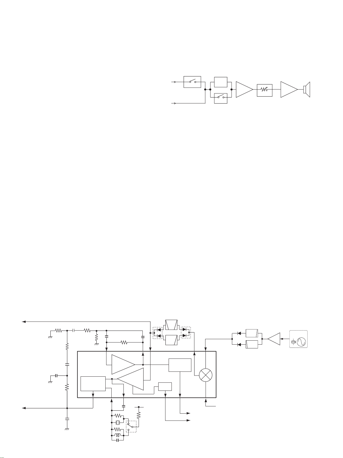
4-1-4 AF AMPLIFIER CIRCUITS (MAIN UNIT)
The demodulated AF signals from the demodulator circuits are
amplified and filtered in AF amplifier circuits.
• FM/WFM mode
The demodulated AF signals from the FM IF IC (IC15, pin 9)
are passed through the AF switch (IC14, pins 1,2) and AF filter
circuit (Q10, D5). The filtered AF signals are applied to the AF
amplifier (Q12).
•AM mode
The demodulated AF signals from the AM-demodulator circuit
(Q19, Q20) are passed through the AF filter bypass switch
(Q28) and applied to the AF amplifier (Q12).
The amplified AF signals are applied to the electric volume
(IC7, pin 11) and level adjusted. The level adjusted AF signals
are output from pin 12, and applied to the AF amplifier (IC9,
pin 2) to obtain more than 50 mW of AF output power. The
power amplified AF signals are then output from pin 6, and
applied to the internal speaker (CHASSIS; SP1) or connected
external speaker via [MIC/SP] connector (J4).
4-1-5 AGC CIRCUIT
A portion of the AM-demodulated signals are converted
into DC voltage, and fed back to the RF circuits as the AGC
(Automatic Gain Controller) signal.
The AGC signal controls the bias of the 1st IF amplifier (Q9)
and RF amplifiers (Q38, Q39, Q42, Q43, Q45) according to
the received signal strength to stabilize the demodulated AF
signal level.
4-1-6 SQUELCH CIRCUITS
•NOISE SQUELCH
The noise squelch mutes the AF output signals when no RF
signals are received. By detecting noise components in the
demodulated AF signals, the squelch circuit toggles the AF
power amplifier ON and OFF.
A portion of the FM-demodulated AF signals from the
FM IF IC (IC15, pin 9) are passed through the noise filter
(R186, R187, R192, R196, R197, R204, C150, C152, C158,
C162, C164). The filtered noise signals are then applied to
the noise amplifier in the FM IF IC (IC15, pins 7, 8) to be
amplified the noise components only.
• AF CIRCUITS
IC14
from
the FM IF IC
(IC15, pin 9)
from the
AM demodulator circuit
(Q19, Q20)
IC7
11 12 2 6
AF switch
Ele. VR
Q12
Q28
12
Q10, D5
AF
Amp. Power
Amp.
IC9
Speaker
AF
Filter
bypass

4 - 3
The amplified noise components are converted into the
pulse-type signal at the noise detector section, and output
from pin 13 as the “NOISE” signal. The “NOISE” signal is
applied to the CPU (IC4, pin 47). Then the CPU outputs
“AFON” signal from pin 68 according to the “NOISE” signal
level to toggle the AF power regulator (Q46, Q47) ON and
OFF.
•TONE SQUELCH
The tone squelch detects the tone signal in the demodulated
AF signals, and opens the squelch only when matched sub-
audible tone frequency is detected in the received signal.
While the tone squelch is in use, and the received signal
contains no sub-audible tone signal or mismatched tone
frequency, the tone squelch mutes the AF signals even if the
noise squelch is open.
A portion of the demodulated AF signals from the FM
IF IC (IC15, pin 9) are passed through the two-staged
CTCSS/DTCS filter (IC5, pins 5, 7 and pins 1, 2) to suppress
unwanted voice signals. The filtered CTCSS/DTCS signals
are applied to the CPU (IC4, pin 7).
The CPU decodes the CTCSS/DTCS signal, and outputs
“AFON” signal from pin 68 according to the set CTCSS/
DTCS signal to toggle the AF power regulator (Q46, Q47)
ON and OFF.
4-2 TRANSMIT CIRCUITS
4-2-1 MICROPHONE AMPLIFIER CIRCUIT (MAIN UNIT)
The microphone amplifier circuit contains AF amplifier, IDC,
splatter filter, etc. The AF signals from the microphone (MIC
signals) are filtered and level-adjusted at this circuit.
The AF signals from the microphone are applied to the MIC
amplifier (IC8, pin 13). The amplified MIC signals are output
from pin 14, and passed through the IDC (Instantaneous
Deviation Control; IC8, pins 8, 9) and splatter filter (IC8, pins
5, 7).
The IDC limits the level of the amplitude of MIC signals to
prevent over deviation, and the splatter filter suppress 3 kHz
and higher audio components. The filtered MIC signals are
passed through the MIC mute switch (Q37) and modulation
volume (Q34).
While receiving, the voltage of R3V line is applied to the
base terminal of the MIC mute switch (Q37) to turn it ON,
thus the MIC line is connected to the ground and the MIC
signals are muted.
The modulation volume (Q34) adjusts the deviation
according to “MODSET” signal from the D/A converter (IC13,
pin 2).
The level adjusted MIC signals are then applied to the
modulation circuit (VCO BOARD; D5 or D6) to modulate the
VCO oscillating signal.
4-2-2 MODULATION CIRCUIT (VCO BOARD)
The modulation circuit modulates the VCO oscillating signal
with the AF signals from the microphone and the tone
signals from the CPU.
•MICROPHONE SIGNALS
The level adjusted MIC signals from the modulation volume
(Q34) are applied to the D5 (in transmitting on 430 MHz
band) or D6 (in transmitting on144 MHz band) to modulate
the VCO oscillating signal by changing the reactance of
D5/D6. The modulated VCO output signal is buffer-amplified
by Q14 and Q19, and applied to the PA BOARD via doubler
switches (D13, D17) and TX/RX switch (MAIN UNIT; D18)
as a transmit signal.
•TONE SIGNALS
The CTCSS and DTCS signals are generated by the CPU
(IC4) and output from pin 141. The CTCSS and DTCS
signals are applied to the modulation circuit (VCO BOARD;
D5 or D6) via the tone filter (Q41). To ensure the modulation,
the DTCS signal is also applied to the the reference
frequency oscillator (X2, pin 1), after passing through the
DTCS filter (IC8, pins 1, 2) and modulation volume (Q48).
4-2-3 TRANSMIT AMPLIFIERS (PA BOARD)
The VCO output signal is amplified to transmit output power
level by the transmit amplifiers.
The VCO output signal from VCO BOARD is passed through
the TX/RX switch (MAIN UNIT; D18) and level adjust circuit
(D1), and applied to the pre-driver (Q1), driver (Q2) and
power (Q3) amplifiers in sequence to be amplified to the
transmit output power level. The power amplified transmit
signal is passed through the antenna switching circuit (MAIN
UNIT; D34, D35) and filters.
4-2-4 TRANSMIT FILTERS (MAIN UNIT)
The power amplified transmit signal from the PA BOARD
is filtered at the transmit filters. The transmit filters prevent
unwanted RF signals being emitted to the air.
While transmitting on 144 MHz band, the transmit signal is
passed through the LPF (L12, C223, C227), antenna switch
circuit (D35, D38), a couple of LPF (L29, L31, C266, C269,
C276, C283, C514, C516) and HPF (L33, C287, C293), and
two LPFs (L39, L42, C307, C314) before being applied to
the antenna connector (CHASSIS; J1).
IC8 Q37 Q34
Mic.
13 14 98
MIC mute Mod. VR
to the VCO
IDC SPLAT-
TER
MIC
57
• MICROPHONE AMPLIFIER CIRCUITS
• 144 MHz
to the antenna
LPF
LPF
LPF
HPF
LPF
from the
PA BOARD
2 LPF’s
D35
ANT
SW
While transmitting on 430 MHz band, the transmit signal
is passed through the HPF (L14, C220, C226), antenna
switching circuit (D34, D37), a couple of LPF (D41, D45, L26,
L30, C255, C257, C262, C275, C282, C289, C515) and HPF
(L38, C302, C306, C310), and the LPF (L42, C314) before
being applied to the antenna connector (CHASSIS; J1).
• 430 MHz
LPF
HPF
LPF
HPF to the antenna
from the
PA BOARD
D34 D41, D45
ANT
SW
4 - 4
Input Register
OSC
Counter
Pre-
scaler
Phase
Detector
Charge
Pump
Loop filter
A
B
Loop filter
X2
15.3 MHz
15.3/45.9 MHz
2nd LO signal
8
Buffer
amp.
Buffer
amp.
LO
amp.
Q19
Doubler
Q18
Q2
Q14
Q29
12
13
14
“PCK”
15
×1
×3
“PUL” signal to the CPU (IC4, pin 35) from the CPU (IC4)
PLL IC control signals
PLL IC (IC15)
VCO BOARD
• PLL AND VCO CIRCUITS
MAIN UNIT
“PDA”
“PSTB”
20
6
1
1
2
2
5
IC19
IC22
5
Q8, Q14, D5
430 MHz VCO
Q10, Q13, D7, D8
50 MHz VCO
Q9, Q12, D6
144 MHz VCO
TCXO
Reference
Counter
LPF
HPF
D51
D52
D12
D13
D16
LO
LV2 LV 1 FIN
D17
×2D18
D56
Transmit signal
to the PA board
1st LO signals to the
1st mixer (IC16, pin 3)
Loop filter
Switch A
Loop filter
Switch B
4-3 PLL CIRCUITS
4-3-1 VCO CIRCUITS (VCO BOARD)
This transceiver has 3 VCOs; 50 MHz VCO, 144 MHz VCO
and 430 MHz VCO. The 50 MHz VCO oscillates the 1st LO
signals, 144 MHz VCO and 430 MHz VCO oscillate both
transmit output and 1st LO signals.
• 50 MHz VCO
The 50 MHz VCO (Q10, Q13, D7, D8) generates the 1st LO
signals for receiving 0.5–76 MHz band signals. The output
signals are amplified at the buffer amplifiers (Q14, Q19),
and passed through the doubler switches (D13, D17), and
then applied to the 1st mixer (IC16, pin 3) via TX/RX switch
(MAIN UNIT; D56).
• 144 MHz VCO
The 144 MHz VCO (Q9, Q12, D6) generates both of transmit
output signal for 144 MHz band and 1st LO signals for
receiving 76–280 MHz.
While receiving, the VCO oscillates the 1st LO frequency,
and the VCO output signals are amplified at the buffer
amplifiers (Q14, Q19). The buffer-amplified signals are
passed through the doubler switches (D13, D17), then
applied to the 1st mixer (IC16, pin 3) via TX/RX switch
(MAIN UNIT; D56).
While transmitting, the VCO oscillates the transmit frequency,
and the VCO output signal is amplified at the buffer amplifiers
(Q14, Q19). The buffer-amplified signals are passed through
the doubler switches (D13, D17), then applied to the PA
BOARD via TX/RX switch (MAIN UNIT; D18).
• 430 MHz VCO
The 430 MHz VCO (Q8, Q11, D5) generates both of the
transmit output signal for 430 MHz band and 1st LO signals
for receiving 280–990 MHz.
While receiving, the VCO oscillates the 1st LO frequency,
and the VCO output signals are amplified by the buffer
amplifiers (Q14, Q19).
If the receiving frequency is 500 MHz and below, the buffer-
amplified signals are passed through the doubler switches
(D13, D17), then applied to the 1st mixer (IC16, pin 3) via
TX/RX switch (MAIN UNIT; D56).
If the receiving frequency is 500 MHz and above, the buffer-
amplified signals are applied to the doubler circuit (Q18,
D14, D15) via doubler switch (D12). The doubled signals are
then applied to the 1st mixer (IC16, pin 3) via doubler switch
(D16) and TX/RX switch (MAIN UNIT; D56).
While transmitting, The VCO oscillates the transmit
frequency, and the VCO output signal is amplified at the
buffer amplifiers (Q14, Q19), then applied to the PA BOARD
via TX/RX switch (MAIN UNIT; D18).
A portion of the VCO output signals generated at each VCO
are applied to the PLL IC (IC18, pin 5) via buffer amplifier
(Q14) and LO amplifier (Q2) for comparison signal.
4-3-2 PLL CIRCUIT
The PLL circuit provides stable oscillation of the transmit
frequency and receive 1st LO frequency. The PLL circuit
compares the phase of the divided VCO frequency with the
reference frequency. The PLL output frequency is controlled
by the divided ratio (N-data) from the CPU.
The amplified signals from LO amplifier (Q2) are applied to
the PLL IC (IC18, pin 5). The applied signals are divided at
the prescaler and OSC counter according to the “PDA” signal
from the CPU (IC4, pin 32). The divided signal is phase-
compared with the reference frequency at the phase detector.
The phase difference is output from pin 20 as a pulse type
signal after being passed through the charge pump and loop
filter switch. The output signal is applied to the each VCO
(VCO BOARD) after being converted into the DC voltage (lock
voltage) at the loop filters.
The lock voltage for 50 MHz VCO (“LV1”) is generated by
being passed through the the loop filter A (Q11, Q13, R68,
R72, R74, R76, R80, R81, C72, C79, C80, C500) via the
loop filter switch A (IC22, pins 5, 6). The lock voltage for
144 MHz VCO and 430 MHz (“LV2”) is generated by being
passed through the loop filter B (Q54, Q56, R327–R331,
R337, C485, C486, C488, C501) via the loop filter switch A
(IC22, pins 1, 2) and B (IC19, pins 1, 2).
If the oscillated signal drifts, its phase changes from that of
the reference frequency, causing a lock voltage change to
compensate for the drift in the oscillated frequency.

4 - 5
Pin
No.
Port
Name Description
2 K2 Input port for [Y], [Z]keys.
3 K1 Input port for [BAND], [CALL] and [V/M] keys.
4 RSSI Input port for RSSI signal for the S-meter
indicator from FM IF IC (IC15, pin 12).
5 VIN Input port for volatage detection of attached
battery pack.
6 CTONE Input port for WX signal.
7 RTONE Input port for CTCSS/DTCS signal.
14 ESIO I/O port for EEPROM (IC1) data.
15 ECK I/O port for the EEPROM (IC1) clock.
25 POWER Input port for [PWR] key (S6).
LOW: When the key is pushed.
26 DSTB Outputs strobe signal to the D/A converter
(IC13, pin 8).
28 CLS Outputs clock sift signal to the clock
frequency shift circuit (Q5).
29 VSTB Outputs VOL strobe signal to the electronic
VR (IC7, pin 14).
32 PDA
Outputs serial data to the PLL IC (IC18, pin 13),
electronic VR (IC7, pin 16) and D/A converter
(IC13, pin 6).
33 PSTB Outputs PLL strobe signal to the PLL IC
(IC18, pin14).
34 PCK
Outputs serial clock signal to the PLL IC
(IC18, pin 12), electronic VR (IC7, pin 15) and
D/A converter (IC13, pin 7).
35 PUL Inputs PLL unlock signal ("PUL") from PLL IC
(IC18, pin15).
41 LEDR
Outputs TX indicator LED (DS8; Red) control
signal to the LED driver (Q49).
"High": While transmitting.
42 LEDG
Outputs RX indicator LED (DS8; Green)
control signal to the LED driver (Q49).
"High": While receiving.
43 UHFC
Outputs UHF RF circuit control signal to the
band selector (Q36).
"High": While receiving on the UHF band.
44 R3C
Outputs receive circuit control signal to R3V
regulator (Q6).
"High": While receiving.
45 WFM
Outputs receiving mode (FM/WFM) switching
signal to the FM/WFM switches (Q16, Q17,
Q51, Q52).
"Low": While receiving in FM mode.
46 AM
Outputs receiving mode (AM/FM) switching
signal to the AM demodulator switch (Q18)
and AF switch (IC14).
"High": While receiving in AM mode.
47 NOISE Inputs "NOISE" signal from the FM IF IC
(IC15, pin 13).
48 DTCS Outputs DTCS filter control signal to the
DTCS filter (Q41).
49 TCON Outputs tone filter control (IC5) signal to the
CTCSS filter switch (Q8).
Pin
No.
Port
Name Description
51 VHFC
Outputs VHF RF circuit control signal to the
band selector (Q36).
"High": While receiving on the VHF band
(76−300 MHz).
52 PCON
Outputs +3V line control signal to the +3V
regulator (IC10).
"High": While the transceiver's power is ON.
53 +3SC Outputs +3S line control signal to the +3S
regulator (Q3, Q4).
54 TXC
Outputs transmit circuits control signal to T3
regulator circuit (Q24–Q27).
"High": While transmitting.
55 BEEP
• While receiving, outputs beep sound to the
electric volume (IC7, pin6).
• While transmitting, outputs 1750 Hz tone signal
to the microphone amplifier circuit (IC8, pin 9).
56 TXU
Outputs UHF TX circuit control signal to TX
band switch (Q27).
"High": While transmitting on UHF band.
57 TXV
Outputs VHF TX circuits control signal to TX
band switch (Q27).
"High": While transmitting on VHF band.
58 VSHIFT
Outputs oscilating frequency shift circuit
(VCO BOARD; Q5, D2–D4) control signal.
"High": D2–D4 are ON, and the oscillating
frequency is shifts down.
59 DBL2
Outputs doubler switches (VCO BOARD;
D13, D17) control signal.
"High":While receiving 500 MHz and below.
60 DBL1
Outputs doubler switches (VCO BOARD;
D12, D16) control signal.
"Low":While receiving 500 MHz and above.
61 ATT
Outputs attenuator control signal to the
attenuator controller (Q40).
"High":While attenuator is activated.
63 HFC Outputs HF RF circuit control signal to the
HF band selector (Q35).
64 BCC Outputs 0.5–30MHz receive circuit control
signal to the HF band selector (Q35).
65 V3C Outputs 430 MHz VCO control signal to the
430 MHz VCO switch (VCO BOARD; Q3).
66 V2C Outputs 144 MHz VCO control signal to the
144 MHz VCO switch (VCO BOARD; Q3).
67 V1C Outputs 50 MHz VCO control signal to the
50 MHz VCO switch (VCO BOARD; Q4).
68 AFON
Outputs AF power amplifier (IC9) control signal
to the AF power amplifier controller (Q46, Q47).
"High": While the audio is emitted.
69 LIGHT
Outputs backlight control signal to the LCD
backlight (PA BOARD; DS1) driver (Q22).
"High": While the backlight is ON.
70 MMUTE
Outputs MIC line mute signal to the MIC
mute switch (Q37).
"High": MIC signal is muted.
71 800C Outputs 500–999 MHz RF circuit control
signal to the 800 MHz band selector (Q40).
73,
74
DUD,
DCK Input ports for [DIAL].
4-4 PORT ALLOCATIONS
4-4-1 CPU (MAIN UNIT; IC4)

4 - 6
Pin
No.
Port
Name Description
75 SQL Input port for [SQL] key (S7).
"Low": While [SQL] is pushed.
76 FUNC Input port for [FUNC] key (PA BOARD; S1).
"Low": While [FUNC] is pushed.
77 PTT Input port for [PTT] key. (PA BOARD; S2)
"Low": While [PTT] is pushed.
138 PSET Outputs transmit power control signal to the
TX power controller (IC17. pin 3).
139 TRAC Outputs BPFs tracking control signal to the
tracking varactor diodes driver (Q32).
141 CTCOUT Outputs CTCSS/DTCS signal to the MIC line.
144 TEMP Input port for internal temperature of the
transceiver.
Line Description
VCC The same voltage as attached battery pack.
CPU3V
Common 3 V converted from VCC line at the
CPU3 regulator (IC11).
The converted voltage is applied to the CPU (IC4),
Re-set IC (IC2), EEPROM (IC1), etc.
+3S
Common 3 V converted from VCCline at the +3S
regulator (Q3, Q4) controlled by "+3SC" signal
from CPU (IC4, pin 53) controlled by "PCON" sig-
nal from the CPU (IC4, pin 52).
The converted voltage is applied to the electric
volume (IC7), VCO BOARD, etc.
+3V
Common 3 V converted from VCCline at the +3V
regulator (IC10, Q1).
The converted voltage is applied to the R3v
regulator (Q6), +10 V DC-DC up-converter (Q7,
Q61, Q62, D3, X4), PLL IC (IC15), D/A converter
(IC13), etc.
R3V
Rceive 3 V controlled by R3V regulator (Q6) using
"R3C" signal from the CPU (IC4, pin 44).
The voltage is applied to the FM IF IC (IC15), 1st
mixer (IC16), 1st IF amplifier (Q9), RF circuits, etc.
TX3
Transmit 3 V controlled by T3 regulator (Q24-Q26)
using "TXC" signal from the CPU (IC4, pin 54).
The controlled voltage is applied to the TX power
controller IC17, Q31, Q50), pre-driver (PA BOARD;
Q1), microphone amplifier (IC8), etc.
+10V
Common +10 V boosted at the +10V DC-DC up-
converter (Q7, Q61, Q62, D3, X4).
The boosted voltage is applied to the loop filters,
tracking vactor diodes driver (Q32), etc.
4-4-2 D/A CONVERTER (MAIN UNIT; IC13)
Pin
No.
Port
Name Description
1 FSET Outputs reference frequency control signal to
the TCXO (X2, pin 1).
2 MODSET Outputs modulation level control signal to the
modulation volume circuit (Q37).
3 DTCSET Outputs DTCS modulation level control signal
to the DTCS modulation volume circuit (Q48).
4-5 POWER SUPPLY CIRCUITS
4-4-1 CPU (MAIN UNIT; IC4)-continue

&-
DEVIATIONMETER /SCIILOSCOPE
!TTENUATOR
D"ORD"
&REQUENCY
COUNTER
TOTHEANTENNACONNECTOR
s*)'CABLE
3TANDARDSIGNALGENERATOR
§6TOM6
nD"MTOnD"M
#!54)/.
$/./4TRANSMITWHILE
THE33'ISCONNECTEDTO
THEANTENNACONNECTOR
!UDIOGENERATOR
(ZTOK(Z
!#
MILLIVOLTMETER
TOTHE;-)#30=JACK
2&POWERMETER
77
3PEAKER7
3
30
-)#
'.$'.$
#,/.%
044
K7
5 - 1
SECTION 5 ADJUSTMENT PROCEDURES
¤ REQUIRED TEST EQUIPMENTS
EQUIPMENT GRADE AND RANGE EQUIPMENT GRADE AND RANGE
RF power meter
(terminated type)
Measuring range : 0.1–3 W
Frequency range : 100–500 MHz
Impedance : 50 Ω
SWR : Less than 1.2 : 1
Standard signal
generator (SSG)
Frequency range : 0.1–1300 MHz
Output level : 0.1 µV to 32 mV
(–127 to –17 dBm)
Frequency counter
Frequency range : 0.1–500 MHz
Frequency accuracy: ±1 ppm or better
Sensitivity : 100 mV or better
Oscilloscope Frequency range : DC–20 MHz
Measuring range : 0.01–20 V
FM deviation meter Frequency range : 30–500 MHz
Measuring range : 0 to ±10 kHz AC millivoltmeter Measuring range : 10 mV to 10 V
Audio generator
Frequency range : 300–3000 Hz
Output level : 1–500 mV
(–47 to 7 dBm)
External speaker Input impedance : 8 Ω
Capacity : More than 50 mW
Attenuator Power attenuation : 20 or 30 dB
Capacity : More than 3 W
5-1 PREPARATION
When adjusting IC-E7, these test equipments and the JIG cable (see the illust below) are required.
¤CONNECTION

5 - 2
¤ ENTERING ADJUSTMENT MODE
qTurn the power OFF.
wConnect the JIG cable (see page 5-1) to the [MIC/SP] jack.
eTurn the "S1" of the JIG cable ON.
rWhile pushing [FUNC], [BAND] and [Y] key, turn the
power ON.
tTurn the "S1" of the JIG cable OFF, then start the adjust
ment.
During adjustment mode, the function dispaly shows the ad-
justment item, frequency, etc. as below.
&-
!DJUSTMENTITEM
!DJUSTMENTFREQUENCY
¤ QUITING ADJUSTMENT MODE
• Turn the power OFF.
¤ KEY ASSIGNMENTS FOR ADJUSTMENT MODE
• : Selects the next adjustment item.
• : Selects the previous adjustment item.
• [DIAL] : Adjusts the value for the item manually.
• + : Adjusts the value for the item automatically.
• : Stores the set value.
NOTE: The set value storing is inhibited
during transmit. Release PTT
switch to return to receive first,
then push this key to store the
set value.
3#!.
3-7

5 - 3
ADJUSTMENT ITEM ADJUSTMENT CONDITION VALUE
REFERENCE
FREQUENCY
[Fr]
1•
•
•
Connect an RF power meter to the antenna connector.
Loosely couple a frequency counter to the antenna connector.
Transmitting
440.00000 MHz
TX HIGH POWER
(VHF/Low band)
[PH1]
1•
•
Connect an RF power meter to the antenna connector.
Transmitting
1.5 W(VHF/Mid band)
[PH2]
2• Transmitting
(VHF/High band)
[PH3]
3• Transmitting
(UHF/Low band)
[PH4]
4• Transmitting
1.0 W
(UHF/Mid band)
[PH5]
5• Transmitting
(UHF/High band)
[PH6]
6• Transmitting
TX LOW POWER
(VHF/Low band)
[PL1]
1• Transmitting
0.1 W
(VHF/Mid band)
[PL2]
2• Transmitting
(VHF/High band)
[PL3]
3• Transmitting
(UHF/Low band)
[PL4]
4• Transmitting
(UHF/Mid band)
[PL5]
5• Transmitting
(UHF/High band)
[PL6]
6• Transmitting
DEVIATION
(VHF/Low band)
[dE1]
1•
•
•
Connect an audio generator to the [MIC/SP] jack through the JIG cable (see
the page 5-1) and set as;
Frequency : 1.0 kHz
Level : 90 mVrms (−8 dBm)
Connect a modulation analyzer to the antenna connector through an
attenuator and set as;
LPF : 20 kHz
HPF : OFF
De-emphasis : OFF
Detector : (P–P)/2
Transmitting
±4.2 kHz
(VHF/Mid band)
[dE2]
2• Transmitting
(VHF/High band)
[dE3]
3• Transmitting
(UHF/Low band)
[dE4]
4• Transmitting
(UHF/Mid band)
[dE5]
5• Transmitting
(UHF/High band)
[dE6]
6• Transmitting
5-2 FREQUENCY AND TRANSMIT ADJUSTMENT
• Set the specified value using [DIAL], and push [BAND] to store the set value. Then push [CALL] to move to the next adjustment item.
NOTE: "REFERENCE FREQUENCY" should be adjusted before "DEVIATION" and "RX SENSITIVITY," and "DEVIATION" should
be adjusted before "DTCS BALANCE" (on the next page). Otherwise, these adjustments will not be adjusted properly.

5 - 4
ADJUSTMENT ITEM ADJUSTMENT CONDITION VALUE
DTCS LEVEL
(VHF)
[dt1]
1• Push [CALL] (No adjustment)
−
(UHF)
[dt2]
2• Push [CALL] (No adjustment)
DTCS BALANCE
(VHF)
[db1]
1•
•
•
No audio signal is applied to the [MIC/SP] jack.
Connect a modulation analyzer with an osciloscope to the antenna connec-
tor through an attenuator, and set the modulation analyzer as;
HPF : OFF De-emphasis : OFF
LPF : 20 kHz Detector : (P–P)/2
Transmitting
Set to square wave
form
(UHF)
[db2]
2• Transmitting
CTCSS DEVIATION
(VHF)
[Ct1]
1•
•
•
No audio signal is applied to the [MIC/SP] jack.
Set the modulation analyzer as the same as "DTCS BALANCE".
Transmitting ±0.75 kHz
(UHF)
[Ct2]
2• Transmitting
RX SENSITIVITY
[t11]
1•
•
Connect an SSG to the antenna connector and set as;
Frequency : Specified frequency* Level : 0 dBµ† (−107 dBm)
Receiving
Push [FUNC]+[BAND]
(Automatic adjustment)
[t21] 2 •
•
Set the SSG as;
Frequency : Specified frequency*
Receiving
[t31] 3 •
•
Set the SSG as;
Frequency : Specified frequency*
Receiving
[t12] 4 •
•
Set the SSG as;
Frequency : Specified frequency*
Receiving
[t22] 5 •
•
Set the SSG as;
Frequency : Specified frequency*
Receiving
[t32] 6 •
•
Set the SSG as;
Frequency : Specified frequency*
Receiving
[t13] 7 •
•
Set the SSG as;
Frequency : Specified frequency*
Receiving
[t23] 8 •
•
Set the SSG as;
Frequency : Specified frequency*
Receiving
[t33] 9 •
•
Set the SSG as;
Frequency : Specified frequency*
Receiving
[t14] 10 •
•
Set the SSG as;
Frequency : Specified frequency*
Receiving
[t24] 11 •
•
Set the SSG as;
Frequency : Specified frequency*
Receiving
[t34] 12 •
•
Set the SSG as;
Frequency : Specified frequency*
Receiving
5-3 SIGNALING AND RECEIVE ADJUSTMENT
• Set the specified value using [DIAL], and push [BAND] to store the set value. Then, push [CALL] to move to the next adjustment item.
NOTE: "DTCS BALANCE" should be adjusted before "CTCSS DEVIATION," and "RX SENSITIVITY" should be adjusted before
"FM/WFM S-METER" (on the next page). Otherwise, these adjustments will not be adjusted properly.
*Displayed on the function display.
†The output level of the standard signal generator (SSG) is indicated as the SSG’s open circuit.

5 - 5
ADJUSTMENT ITEM ADJUSTMENT CONDITION VALUE
[t44] 13 •
•
Set the SSG as;
Frequency : Specified frequency*
Receiving Push [FUNC]+[BAND]
(Automatic adjustment)
[t54] 14 •
•
Set the SSG as;
Frequency : Specified frequency*
Receiving
[t64] 15 •
•
Set the SSG as;
Frequency : Specified frequency*
Receiving
Push [FUNC]+[BAND]
(Automatic adjustment)
[t15] 16 •
•
Set the SSG as;
Frequency : Specified frequency*
Receiving
[t25] 17 •
•
Set the SSG as;
Frequency : Specified frequency*
Receiving
[t35] 18 •
•
Set the SSG as;
Frequency : Specified frequency*
Receiving
[t45] 19 •
•
Set the SSG as;
Frequency : Specified frequency*
Receiving
FM S-METER
[S1]
1•
•
Set the SSG as;
Frequency : Specified frequency* Level : 0 dBµ† (−107 dBm)
Receiving
Push [BAND]
[S2] 2 •
•
Set the SSG as;
Frequency : Specified frequency*
Receiving
[S3] 3 •
•
Set the SSG as;
Frequency : Specified frequency*
Receiving
[S4] 4 •
•
Set the SSG as;
Frequency : Specified frequency*
Receiving
[S5L] 5 •
•
Set the SSG as;
Frequency : Specified frequency*
Receiving
[S5H] 6 •
•
Set the SSG as;
Frequency : Specified frequency*
Receiving
[S6] 7 •
•
Set the SSG as;
Frequency : Specified frequency* Level : +5 dBµ† (−102 dBm)
Receiving
WFM S-METER
[S2]
1•
•
Set the SSG as;
Frequency : Specified frequency* Level : +1 dBµ† (−106 dBm)
Receiving
Push [BAND]
[S3] 2 •
•
Set the SSG as;
Frequency : Specified frequency* Level : −3 dBµ† (−104 dBm)
Receiving
[S4] 3 •
•
Set the SSG as;
Frequency : Specified frequency*
Receiving
[S5L] 4 •
•
Set the SSG as;
Frequency : Specified frequency*
Receiving
[S5H] 5 •
•
Set the SSG as;
Frequency : Specified frequency*
Receiving
[S6] 6 •
•
Set the SSG as;
Frequency : Specified frequency* Level : +8 dBµ† (−99 dBm)
Receiving
• RECEIVE ADJUSTMENT (continued)
*Displayed on the function display.
†The output level of the standard signal generator (SSG) is indicated as the SSG’s open circuit.

6 - 1
SECTION 6 PARTS LIST
M.=Mounted side (T: Mounted on the Top side, B: Mounted on the Bottom side)
S.=Surface mount
[MAIN UNIT]
REF ORDER DESCRIPTION M. H/V
NO. NO.
LOCATION
IC1 1130012690 S.IC HN58X24256FPIE (SOP8) T 11.5/61.9
IC2 1110006720 S.IC R3112N291A-TR-F T 9.3/46.2
1140013010 S.IC M30220FCRP T 27/53.5
IC5 1110006380 S.IC LM2904PWR T 21.1/26.5
IC7 1130011860 S.IC SM6451BT-G-E2 B 22.7/10
IC8 1110006470 S.IC LMV324IPWR T 15/21.8
IC9 1110002810 S.IC NJM2070M-TE1 B 26.5/59.9
IC10 1180002371 S.REG R1111N321B-TR-F B 4.5/34.3
IC11 1180002371 S.REG R1111N321B-TR-F T 36.5/61.9
IC12 1130007111 S.IC TC7W04FU (TE12L,F) T 27.2/70.1
IC13 1190001830 S.IC BH2220FVM-TR T 29.1/25
IC14 1130004201 S.IC TC4S66F T 35.7/21.3
IC15 1110003201 S.IC TA31136FNG (EL)
[ITR], [EXP], [FRA] only B 34.4/20.4
IC16 1110005230 S.IC µPC2757TB-E3 B 34.7/45.5
IC17 1110006490 S.IC LMV321IDCKR T 7.4/62.7
IC18 1130012980 S.IC ADF4110BCPZ B 9.9/17.1
IC19 1130007021 S.IC TC7S66F B 7/8.2
IC22 1130009581 S.IC TC7W66FU B 4/6.3
Q1 1590003230 S.TR UNR9113J-(TX) T 37.5/59
Q2 1530003630 S.TR 2SC4617 TLS B 3.5/2.7
Q3 1590001170 S.TR XP1501-(TX) AB T 28/4.1
Q4 1510000671 S.TR 2SA1588 GR T 28.4/6.7
Q5 1590003290 S.TR UNR9213J-(TX) T 16.4/45.5
Q6 1510000671 S.TR 2SA1588 GR T 25.2/6.1
Q7 1530003630 S.TR 2SC4617 TLS B 28.1/36.8
Q8 1590003250 S.TR UNR9115J-(TX) T 21.3/33.8
Q9 1530003260 S.TR 2SC5006-T1 B 32.3/31.2
Q10 1590001190 S.TR XP6501-(TX) AB T 30.8/13.6
Q11 1560000541 S.TR 2SK880 Y T 18.8/9.8
Q12 1530003630 S.TR 2SC4617 TLS T 23/13.7
Q13 1530003630 S.TR 2SC4617 TLS T 22.1/8.2
Q14 1510001100 S.TR 2SA1832-GR T 39.8/50
Q16 1590002010 S.TR XP1114 (TX) B 36.6/3.3
Q17 1590003290 S.TR UNR9213J-(TX) T 34.3/3.9
Q18 1590003250 S.TR UNR9115J-(TX) T 39.4/12.3
Q19 1590001190 S.TR XP6501-(TX) AB T 35.7/14.9
Q20 1590001190 S.TR XP6501-(TX) AB T 35/11.3
Q22 1530003630 S.TR 2SC4617 TLS T 16.7/69.6
Q24 1590003280 S.TR UNR9211J-(TX) T 25.2/16.9
Q25 1590001170 S.TR XP1501-(TX) AB T 23.3/18.9
Q26 1510000620 S.TR 2SA1576 T106 S T 20.7/19.1
Q27 1590001810 S.TR XP1113 (TX) T 7/50.2
Q28 1590001451 S.FET 2SJ144-GR (TE85R,F) [UK] only B 23.9/15.6
Q29 1530003630 S.TR 2SC4617 TLS B 22.8/21.2
Q30 1590001650 S.TR XP4601 (TX) T 31.8/71.5
Q31 1590002160 S.TR XP6401-(TX) T 12.4/55.4
Q32 1590001650 S.TR XP4601 (TX) B 25.2/36.6
Q34 1590001451 S.FET 2SJ144-GR (TE85R,F) [UK] only T 16.3/13.2
Q35 1590001810 S.TR XP1113 (TX) B 27.8/40.5
Q36 1590001810 S.TR XP1113 (TX) B 4.2/37.3
Q37 1530003091 S.TR 2SC4213-B (TE85R,F) T 18.2/15
Q38 1530003260 S.TR 2SC5006-T1 B 24.5/47.4
Q39 1530003591 S.TR 2SC5277-D2-TL-E B 24.8/44.5
Q40 1590001810 S.TR XP1113 (TX) T 39/44.5
Q41 1590003290 S.TR UNR9213J-(TX) T 28.5/30.6
Q42 1530003611 S.TR FH102-TR-E B 10.9/41
Q43 1530003611 S.TR FH102-TR-E B 6.9/40.9
Q44 1590003290 S.TR UNR9213J-(TX) B 3.1/57.5
Q45 1530003591 S.TR 2SC5277-D2-TL-E B 16.1/45
Q46 1590001170 S.TR XP1501-(TX) AB B 37.7/56.3
Q47 1510000620 S.TR 2SA1576 T106 S B 36.8/59
Q48 1590001451 S.FET 2SJ144-GR (TE85R,F) [UK] only T 31.1/18.9
Q49 1590002700 S.TR XP4214 (TX) T 35/71.5
Q50 1590003390 S.TR UNR9215J-(TX) T 12.6/52.8
Q51 1590002010 S.TR XP1114 (TX) B 27.4/25
Q52 1590003290 S.TR UNR9213J-(TX) B 24.6/27.7
Q54 1560000541 S.TR 2SK880 Y T 19.4/7.2
Q56 1530003630 S.TR 2SC4617 TLS T 20.8/4
Q59 1590003230 S.TR UNR9113J-(TX) T 16.3/4.9
Q60 1590001680 S.TR XP1110 (TX) T 23.2/4.1
Q61 1530003630 S.TR 2SC4617 TLS B 19.9/27.2
Q62 1530003630 S.TR 2SC4617 TLS B 22.4/25
D3 1790001790 S.DIO RB876W TL B 23.8/31.1
D4 1790001790 S.DIO RB876W TL B 25.8/31.1
D5 1750000940 S.DIO ISS400 TE61 T 27.5/11.1
D6 1730002320 S.ZEN MA8051-M (TX) B 14.9/26.1
D9 1790001240 S.DIO MA2S728-(TX) T 32.9/9.7
D10 1750001070 S.DIO DAN235ETL T 30.6/8.3
D11 1750000940 S.DIO ISS400 TE61 T 19/69
D12 1750001070 S.DIO DAN235ETL T 39.5/16.9
D13 1790001250 S.DIO MA2S111-(TX) B 29.2/30.3
D14 1750001070 S.DIO DAN235ETL B 30.3/33.8
D16 1790001621 S.DIO 1SV308 B 31.2/47.8
[MAIN UNIT]
REF ORDER DESCRIPTION M. H/V
NO. NO.
LOCATION
D17 1750001070 S.DIO DAN235ETL B 37.2/41.9
D18 1750001070 S.DIO DAN235ETL B 16.1/22.3
D21 1790001621 S.DIO 1SV308 B 22/40
D22 1790001621 S.DIO 1SV308 B 17/34.6
D23 1790001621 S.DIO 1SV308 B 30.1/45.5
D24 1750000940 S.DIO ISS400 TE61 B 25.4/38.5
D25 1790001590 S.DIO MA6S718 (TX) B 25.3/40.5
D26 1750000721 S.VCP HVC375BTRF-E B 11.9/34
D27 1790001260 S.DIO MA2S077-(TX) B 19.7/37.8
D28 1720000840 S.VCP HVD328CKRU-E B 16.8/38.5
D29 1750000520 S.DIO DAN222TL B 30.2/43.8
D30 1750001070 S.DIO DAN235ETL B 21.3/47
D31 1720000840 S.VCP HVD328CKRU-E B 14.8/37.7
D32 1750000721 S.VCP HVC375BTRF-E B 7.4/33.6
D33 1720000840 S.VCP HVD328CKRU-E B 21.1/43.2
D34 1790001621 S.DIO 1SV308 B 7.8/55.9
D35 1790001621 S.DIO 1SV308 B 11.2/53.2
D36 1790001260 S.DIO MA2S077-(TX) B 9.4/38.9
D37 1790001621 S.DIO 1SV308 B 2.7/55.7
D38 1790001621 S.DIO 1SV308 B 10.7/58.7
D39 1720000840 S.VCP HVD328CKRU-E B 16.8/47.6
D40 1720000840 S.VCP HVD328CKRU-E B 18.2/42.8
D41 1790001621 S.DIO 1SV308 B 5.6/57.8
D43 1750001070 S.DIO DAN235ETL B 18.3/51.1
D44 1790001621 S.DIO 1SV308 B 19.6/56.1
D45 1790001621 S.DIO 1SV308 B 5.1/63.5
D46 1790001621 S.DIO 1SV308 B 12.8/49.7
D50 1750000370 S.DIO DA221 TL B 27.2/51.5
D51 1790001621 S.DIO 1SV308 B 31/21
D52 1790001621 S.DIO 1SV308 B 28.9/20.2
D53 1790001621 S.DIO 1SV308 B 8.6/45.4
D54 1790001621 S.DIO 1SV308 B 14.5/52.8
D55 1750000711 S.VCP HVC350BTRF-E B 3.7/44.6
FI1 2020002170 S.CER ELFY450E B 31.8/8.5
FI2 2020002200 S.CER SFECS14M8DA0001 B 31.2/38.5
FI3 2010002670 S.XTL FL-393 (46.350 MHz) B 36.5/35.5
X1 6050012240 S.XTL CR-813 (7.325 MHz) T 13.7/48.2
X2 6050012170 S.XTL CR-807 (15.3 MHz) B 11.1/21.6
X3 6070000190 S.DCR CDBCB450KCAY24-R0 B 37.7/27.7
X4 6060000800 S.CER CSTCR6M75G53 B 20/30.7
L1 6200003640 S.COL MLF1608E 100K-T B 16.8/27.5
L2 6200005500 S.COL NL 322522T-471J B 39.1/13.1
L3 6200007170 S.COL MLF1608A 3R3K-T B 32.4/28.6
L4 6200002040 S.COL NL 252018T-J B 27/47.8
L5 6200003540 S.COL MLF1608D R22K-T B 24/19.1
L6 6200003630 S.COL MLF1608D R68K-T B 26.1/21.3
L7 6200004660 S.COL MLF1608A 1R8K-T B 30.9/41.2
L8 6200005641 S.COL ELJRE 6N8ZFA B 31.9/46.5
L9 6200005721 S.COL ELJRE 33NGFA B 26.5/44.8
L10 6200011590 S.COL LQW18AN39NG00D B 17.9/38.5
L11 6200011650 S.COL LQW18AN68NG00D B 19/36.5
L12 6200008530 S.COL 0.30-1.0-4TR 12N B 8.8/49.9
L13 6200009220 S.COL LQW18AN15NG00D B 10/33.4
L14 6200009110 S.COL 0.30-0.9-2TR 4.1N B 6.2/52.6
L15 6200006040 S.COL LQP18MN5N6C02D B 22.2/43.3
L16 6200004590 S.COL MLF1608D R18K-T B 7.8/58.4
L17 6200004590 S.COL MLF1608D R18K-T B 10.9/50.9
L18 6200010210 S.COL C2012C-22NG-A B 6/55.3
L19 6200010000 S.COL C2012C-56NG-A B 12.1/55.9
L20 6200003540 S.COL MLF1608D R22K-T B 18.9/48.7
L21 6200005200 S.COL ELJNC R68K-F B 18.8/45.1
L22 6200011590 S.COL LQW18AN39NG00D B 12.8/38.9
L23 6200010910 S.COL LQW18AN56NG00D B 10.5/37.7
L24 6200004930 S.COL MLF1608E 8R2K-T B 16.6/51.3
L25 6200009220 S.COL LQW18AN15NG00D B 7/38
L26 6200008220 S.COL 0.40-1.4-5TR 21N B 5.2/59.7
L27 6200006040 S.COL LQP18MN5N6C02D B 17/41.7
L28 6200005721 S.COL ELJRE 33NGFA B 15.2/42.4
L29 6200008170 S.COL 0.35-1.6-8TL 54N B 16.2/56
L30 6200008270 S.COL 0.26-1.0-5TL 17N B 7.4/62.8
L31 6200008260 S.COL 0.30-1.7-8TL 60N B 16.2/59.4
L32 6200009531 S.COL ELJRE R15GFA B 21.2/59.8
L33 6200008190 S.COL 0.25-1.9-8TL 80N B 10.3/62.4
L34 6200009571 S.COL ELJRE R12GFA B 19.4/60.6
L36 6200011580 S.COL LQW18AN33NG00D B 6.1/43.7
L37 6200005671 S.COL ELJRE 12NGFA B 14.9/49.4
L38 6200008220 S.COL 0.40-1.4-5TR 21N B 6.5/65.5
L39 6200008190 S.COL 0.25-1.9-8TL 80N B 11.5/65.8
L40 6200005661 S.COL ELJRE 10NGFA B 12.7/51.9
L41 6200005661 S.COL ELJRE 10NGFA T 10.9/72.6
L42 6200008700 S.COL 0.30-0.9-6TR 17.5N B 10.5/68.7
L43 6200003630 S.COL MLF1608D R68K-T B 24.3/22.6
• IC-E7

6 - 2
M.=Mounted side (T: Mounted on the Top side, B: Mounted on the Bottom side)
S.=Surface mount
[MAIN UNIT]
REF ORDER DESCRIPTION M. H/V
NO. NO.
LOCATION
L44 6200006981 S.COL ELJRE R10GFA B 10.8/43.9
L101 6200003640 S.COL MLF1608E 100K-T T 9.3/53.1
L102 6200004480 S.COL MLF1608D R82K-T T 8.6/58.5
L103 6200005560 S.COL ELJSC K-F B 30.1/27.8
L104 6200009270 S.COL MLF2012K 560K-T B 19.6/25.1
L105 6200003640 S.COL MLF1608E 100K-T B 33.6/57.6
L106 6200011590 S.COL LQW18AN39NG00D B 4.9/44.6
R1 7030005050 S.RES ERJ2GEJ 103 X (10 kΩ) B 6/13.6
R2 7030005050 S.RES ERJ2GEJ 103 X (10 kΩ) B 22.4/58.8
R3 7030005050 S.RES ERJ2GEJ 103 X (10 kΩ) B 3.1/40.5
R4 7030005070 S.RES ERJ2GEJ 683 X (68 kΩ) T 36/64.1
R5 7030006610 S.RES ERJ2GEJ 394 X (390 kΩ) T 11.6/27
R6 7030005100 S.RES ERJ2GEJ 154 X (150 kΩ) B 2/19.6
R7 7030005120 S.RES ERJ2GEJ 102 X (1 kΩ) B 2/3
R8 7030005310 S.RES ERJ2GEJ 124 X (120 kΩ) T 36/65
R9 7030005240 S.RES ERJ2GEJ 473 X (47 kΩ) B 23.3/60.4
R10 7030005240 S.RES ERJ2GEJ 473 X (47 kΩ) B 23.3/58.8
R11 7030005240 S.RES ERJ2GEJ 473 X (47 kΩ) B 23.3/57.2
R12 7030005310 S.RES ERJ2GEJ 124 X (120 kΩ) T 29.6/29
R13 7030005570 S.RES ERJ2GEJ 820 X (82 Ω) T 29.5/32.2
R14 7510001770 S.TMR NTCG10 4LH 473JT B 24.6/55.7
R15 7030005090 S.RES ERJ2GEJ 104 X (100 kΩ) B 26.5/54.4
R16 7030005570 S.RES ERJ2GEJ 820 X (82 Ω) B 8.6/34.9
R17 7030005120 S.RES ERJ2GEJ 102 X (1 kΩ) T 15.1/61.4
R18 7030005120 S.RES ERJ2GEJ 102 X (1 kΩ) T 16.8/58.6
R19 7030005120 S.RES ERJ2GEJ 102 X (1 kΩ) T 15.9/58.1
R20 7030005100 S.RES ERJ2GEJ 154 X (150 kΩ) B 12.5/42.6
R21 7030006610 S.RES ERJ2GEJ 394 X (390 kΩ) B 12.7/41
R22 7030005570 S.RES ERJ2GEJ 820 X (82 Ω) B 4.8/24.4
R23 7030005290 S.RES ERJ2GEJ 682 X (6.8 kΩ) T 27.4/1.8
R24 7030007300 S.RES ERJ2GEJ 332 X (3.3 kΩ) T 26.3/3.2
R25 7030007290 S.RES ERJ2GEJ 222 X (2.2 kΩ) T 28.6/2.2
R26 7030010040 S.RES ERJ2GE-JPW T 18.9/46.9
R27 7030005310 S.RES ERJ2GEJ 124 X (120 kΩ) T 10.9/44
R28 7030005570 S.RES ERJ2GEJ 820 X (82 Ω) B 2/18
R29 7030005240 S.RES ERJ2GEJ 473 X (47 kΩ) T 30.7/5.8
R30 7030005060 S.RES ERJ2GEJ 333 X (33 kΩ) T 29.8/3.4
R31 7030005240 S.RES ERJ2GEJ 473 X (47 kΩ) T 27.9/8.4
R32 7030005040 S.RES ERJ2GEJ 472 X (4.7 kΩ) T 29.1/8.7
R33 7030005120 S.RES ERJ2GEJ 102 X (1 kΩ) B 25.3/54.5
R34 7030005090 S.RES ERJ2GEJ 104 X (100 kΩ) B 28.3/35.3
R35 7030005050 S.RES ERJ2GEJ 103 X (10 kΩ) T 16.9/48.4
R36 7030010040 S.RES ERJ2GE-JPW T 16/48.4
R37 7030005240 S.RES ERJ2GEJ 473 X (47 kΩ) T 16.3/49.9
R38 7030005240 S.RES ERJ2GEJ 473 X (47 kΩ) T 6.6/45
R39 7030005240 S.RES ERJ2GEJ 473 X (47 kΩ) T 4.7/45
R40 7030005160 S.RES ERJ2GEJ 105 X (1 MΩ) T 19.5/33.7
R41 7030005170 S.RES ERJ2GEJ 474 X (470 kΩ) T 18.4/32.5
R43 7030005120 S.RES ERJ2GEJ 102 X (1 kΩ) B 4.9/27.1
R44 7030005120 S.RES ERJ2GEJ 102 X (1 kΩ) B 4/27.3
R49 7030005070 S.RES ERJ2GEJ 683 X (68 kΩ) T 22.1/22.2
R54 7030005120 S.RES ERJ2GEJ 102 X (1 kΩ) B 7.1/13.6
R55 7030005120 S.RES ERJ2GEJ 102 X (1 kΩ) B 8/13.5
R56 7030006610 S.RES ERJ2GEJ 394 X (390 kΩ) T 27.8/16.3
R57 7030008290 S.RES ERJ2GEJ 183 X (18 kΩ) T 27.8/15.4
R58 7030005120 S.RES ERJ2GEJ 102 X (1 kΩ) B 10.2/13.8
R59 7030005090 S.RES ERJ2GEJ 104 X (100 kΩ) B 11.8/13.7
R60 7030007320 S.RES ERJ2GEJ 225 X (2.2 MΩ) T 28.6/18.4
R61 7030005040 S.RES ERJ2GEJ 472 X (4.7 kΩ) T 27.9/14.5
R62 7030007320 S.RES ERJ2GEJ 225 X (2.2 MΩ) T 29.1/14.4
R63 7030008300 S.RES ERJ2GEJ 184 X (180 kΩ) T 29.2/12.2
R64 7030008300 S.RES ERJ2GEJ 184 X (180 kΩ) T 29.9/15.9
R65 7030005170 S.RES ERJ2GEJ 474 X (470 kΩ) T 30.2/17.3
R66 7030008280 S.RES ERJ2GEJ 271 X (270 Ω) B 13.3/16.7
R67 7030005090 S.RES ERJ2GEJ 104 X (100 kΩ) T 31.1/16.4
R68 7030008410 S.RES ERJ2GEJ 392 X (3.9 kΩ) T 17.8/7.8
R69 7030007340 S.RES ERJ2GEJ 153 X (15 kΩ) T 32.3/15.9
R70 7030005160 S.RES ERJ2GEJ 105 X (1 MΩ) T 27.2/13.3
R71 7030005080 S.RES ERJ2GEJ 823 X (82 kΩ) T 30.1/10.7
R72 7030005040 S.RES ERJ2GEJ 472 X (4.7 kΩ) T 12.4/10.5
R73 7030008300 S.RES ERJ2GEJ 184 X (180 kΩ) T 25.5/10.6
R74 7030005290 S.RES ERJ2GEJ 682 X (6.8 kΩ) T 21.3/6.2
R75 7030005170 S.RES ERJ2GEJ 474 X (470 kΩ) T 24.5/13.1
R76 7030005290 S.RES ERJ2GEJ 682 X (6.8 kΩ) T 22.2/6.2
R77 7030005530 S.RES ERJ2GEJ 100 X (10 Ω) T 23.5/11.7
R78 7030008010 S.RES ERJ2GEJ 123 X (12 kΩ) T 21.3/12.7
R79 7030009270 S.RES ERJ2GEJ 821 X (820 Ω) T 21.3/13.9
R80 7030007340 S.RES ERJ2GEJ 153 X (15 kΩ) T 21.6/10.1
R81 7030008410 S.RES ERJ2GEJ 392 X (3.9 kΩ) T 20.7/9.4
R82 7030005160 S.RES ERJ2GEJ 105 X (1 MΩ) T 7.3/60.7
R83 7030005050 S.RES ERJ2GEJ 103 X (10 kΩ) T 5.3/62.2
R84 7030005110 S.RES ERJ2GEJ 224 X (220 kΩ) T 14.9/62.9
R85 7030005710 S.RES ERJ2GEJ 121 X (120 Ω) B 28.7/54.5
R86 7030005120 S.RES ERJ2GEJ 102 X (1 kΩ) T 28/32.8
R87 7030008410 S.RES ERJ2GEJ 392 X (3.9 kΩ) T 25.5/35.8
R88 7030007340 S.RES ERJ2GEJ 153 X (15 kΩ) T 26.1/28.7
R89 7030006610 S.RES ERJ2GEJ 394 X (390 kΩ) T 24.5/28.7
R90 7030005530 S.RES ERJ2GEJ 100 X (10 Ω) B 26.9/64.3
R91 7030005040 S.RES ERJ2GEJ 472 X (4.7 kΩ) T 23.3/26.3
R92 7030005060 S.RES ERJ2GEJ 333 X (33 kΩ) B 14.9/28
R93 7510001480 S.TMR NTCG10 3NH 681JT T 14/10.8
R94 7030005010 S.RES ERJ2GEJ 681 X (680 Ω) T 32/23.4
R95 7030005240 S.RES ERJ2GEJ 473 X (47 kΩ) B 2.4/38.9
R96 7030005240 S.RES ERJ2GEJ 473 X (47 kΩ) T 14.7/59.2
[MAIN UNIT]
REF ORDER DESCRIPTION M. H/V
NO. NO.
LOCATION
R97 7030005050 S.RES ERJ2GEJ 103 X (10 kΩ) T 14.6/57.7
R101 7030005120 S.RES ERJ2GEJ 102 X (1 kΩ) B 24.8/52.7
R104 7030005030 S.RES ERJ2GEJ 152 X (1.5 kΩ) T 37.2/17
R105 7030004980 S.RES ERJ2GEJ X (100 Ω) T 38.2/11.2
R106 7030010040 S.RES ERJ2GE-JPW
[EUR], [ITR], [FRA] only T 39.7/57.8
R107 7030010040 S.RES ERJ2GE-JPW [UK] only T 39.7/56.9
R108 7030007060 S.RES ERJ2GEJ 684X (680 kΩ) T 35.8/16.8
R109 7030005220 S.RES ERJ2GEJ 223 X (22 kΩ) T 37.6/14.8
R110 7030010040 S.RES ERJ2GE-JPW [ITR], [FRA] only T 39.7/56
R111 7030010040 S.RES ERJ2GE-JPW
[FRA] only T 39.7/55.1
R112 7030010040 S.RES ERJ2GE-JPW B 34.5/51.3
R113 7030010040 S.RES ERJ2GE-JPW [ITR], [FRA] only B 33.2/51.3
R114 7030005160 S.RES ERJ2GEJ 105 X (1 MΩ) T 33.7/14.8
R115 7030010040 S.RES ERJ2GE-JPW B 31.9/51.3
R116 7030010040 S.RES ERJ2GE-JPW B 30.6/51.3
R117 7030005090 S.RES ERJ2GEJ 104 X (100 kΩ) T 24.6/72.8
R118 7030005240 S.RES ERJ2GEJ 473 X (47 kΩ) T 34.9/13
R119 7030005090 S.RES ERJ2GEJ 104 X (100 kΩ) T 23.7/72.8
R120 7030005090 S.RES ERJ2GEJ 104 X (100 kΩ) T 36.9/12.7
R121 7030008370 S.RES ERJ2GEJ 561 X (560 Ω) T 37.8/12.4
R122 7030005070 S.RES ERJ2GEJ 683 X (68 kΩ) T 20.7/31.1
R123 7030005090 S.RES ERJ2GEJ 104 X (100 kΩ) B 25.7/51.8
R124 7030008300 S.RES ERJ2GEJ 184 X (180 kΩ) B 28.6/50.7
R125 7030007300 S.RES ERJ2GEJ 332 X (3.3 kΩ) T 36.6/9.7
R126 7030005160 S.RES ERJ2GEJ 105 X (1 MΩ) T 21.9/31.8
R127 7030005050 S.RES ERJ2GEJ 103 X (10 kΩ) T 29.2/72.9
R128 7030005100 S.RES ERJ2GEJ 154 X (150 kΩ) T 35/9.7
R129 7030005100 S.RES ERJ2GEJ 154 X (150 kΩ) T 33.2/11
R130 7030005050 S.RES ERJ2GEJ 103 X (10 kΩ) T 15.8/71.3
R131 7030005050 S.RES ERJ2GEJ 103 X (10 kΩ) T 19.5/70.3
R132 7030005050 S.RES ERJ2GEJ 103 X (10 kΩ) T 20.4/70.3
R133 7030008010 S.RES ERJ2GEJ 123 X (12 kΩ) T 32.3/73.2
R134 7030005080 S.RES ERJ2GEJ 823 X (82 kΩ) T 21.3/21.1
R135 7030005230 S.RES ERJ2GEJ 334 X (330 kΩ) T 15.3/64.1
R157 7030005050 S.RES ERJ2GEJ 103 X (10 kΩ) T 5.3/64.7
R168 7030005040 S.RES ERJ2GEJ 472 X (4.7 kΩ) T 30.6/6.7
R169 7030005080 S.RES ERJ2GEJ 823 X (82 kΩ) T 22.9/21.1
R170 7030007330 S.RES ERJ1WRSJR15U (0.15
Ω) T 6.2/55.7
R171 7030005050 S.RES ERJ2GEJ 103 X (10 kΩ) B 35.8/9.2
R172 7030005080 S.RES ERJ2GEJ 823 X (82 kΩ) T 23.3/22.3
R173 7030007340 S.RES ERJ2GEJ 153 X (15 kΩ) B 36.2/13.2
R174 7030005160 S.RES ERJ2GEJ 105 X (1 MΩ) T 23.2/23.5
R175 7030005170 S.RES ERJ2GEJ 474 X (470 kΩ) T 24.8/23.5
R176 7030005090 S.RES ERJ2GEJ 104 X (100 kΩ) T 22.7/36.2
R177 7030005040 S.RES ERJ2GEJ 472 X (4.7 kΩ) B 39.5/10.9
R178 7030005090 S.RES ERJ2GEJ 104 X (100 kΩ) T 24.3/36.2
R179 7030005050 S.RES ERJ2GEJ 103 X (10 kΩ) B 36.7/9.9
R180 7030005160 S.RES ERJ2GEJ 105 X (1 MΩ) T 18.3/17
R181 7030005700 S.RES ERJ2GEJ 274 X (270 kΩ) T 27.9/21.6
R182 7030007340 S.RES ERJ2GEJ 153 X (15 kΩ) T 26.4/21.3
R183 7030005000 S.RES ERJ2GEJ 471 X (470 Ω) T 23.4/16.8
R184 7030005000 S.RES ERJ2GEJ 471 X (470 Ω) T 20.6/17.4
R185 7030005040 S.RES ERJ2GEJ 472 X (4.7 kΩ) T 40.3/18.4
R186 7030005090 S.RES ERJ2GEJ 104 X (100 kΩ) T 32.9/17.6
R187 7030005030 S.RES ERJ2GEJ 152 X (1.5 kΩ) T 35.8/17.7
R188 7030010040 S.RES ERJ2GE-JPW T 25.1/18.9
R190 7030009160 S.RES ERJ2GEJ 181 X (180 Ω) B 33.4/29.3
R191 7030005030 S.RES ERJ2GEJ 152 X (1.5 kΩ) B 37.7/17.5
R192 7030005240 S.RES ERJ2GEJ 473 X (47 kΩ) T 34.2/18.6
R194 7030005290 S.RES ERJ2GEJ 682 X (6.8 kΩ) B 8/24.4
R195 7030005120 S.RES ERJ2GEJ 102 X (1 kΩ) B 33/32.7
R196 7030007340 S.RES ERJ2GEJ 153 X (15 kΩ) T 33.4/22.2
R197 7030005030 S.RES ERJ2GEJ 152 X (1.5 kΩ) T 33.4/21
R198 7030007340 S.RES ERJ2GEJ 153 X (15 kΩ) B 30.6/30.3
R199 7030005110 S.RES ERJ2GEJ 224 X (220 kΩ) B 30.5/31.2
R200 7030008300 S.RES ERJ2GEJ 184 X (180 kΩ) B 22.7/19.7
R201 7030005170 S.RES ERJ2GEJ 474 X (470 kΩ) T 32.2/11
R202 7030007320 S.RES ERJ2GEJ 225 X (2.2 MΩ) B 25/17.5
R203 7030005050 S.RES ERJ2GEJ 103 X (10 kΩ) B 29.3/32.4
R204 7030005000 S.RES ERJ2GEJ 471 X (470 Ω) T 32/24.3
R205 7030008280 S.RES ERJ2GEJ 271 X (270 Ω) B 25.1/19.9
R206 7030005050 S.RES ERJ2GEJ 103 X (10 kΩ) B 30.9/35.7
R207 7030010040 S.RES ERJ2GE-JPW B 31.8/34.8
R208 7030005050 S.RES ERJ2GEJ 103 X (10 kΩ) B 31.8/33.1
R209 7030005090 S.RES ERJ2GEJ 104 X (100 kΩ) B 30.4/23.3
R211 7030010040 S.RES ERJ2GE-JPW B 25.5/24.6
R213 7030005050 S.RES ERJ2GEJ 103 X (10 kΩ) B 33.3/41.4
R214 7030005010 S.RES ERJ2GEJ 681 X (680 Ω) B 31.8/26
R217 7030005000 S.RES ERJ2GEJ 471 X (470 Ω) B 35.3/41.4
R218 7030008400 S.RES ERJ2GEJ 182 X (1.8 kΩ) T 10/57.8
R220 7030005050 S.RES ERJ2GEJ 103 X (10 kΩ) B 33.9/42.8
R221 7030005050 S.RES ERJ2GEJ 103 X (10 kΩ) B 37.5/40.5
R223 7030005080 S.RES ERJ2GEJ 823 X (82 kΩ) B 23.3/37.3
R224 7030005220 S.RES ERJ2GEJ 223 X (22 kΩ) B 22.9/36.1
R225 7030007290 S.RES ERJ2GEJ 222 X (2.2 kΩ) B 15.4/20.3
R227 7030005050 S.RES ERJ2GEJ 103 X (10 kΩ) B 39.1/40.5
R228 7030005050 S.RES ERJ2GEJ 103 X (10 kΩ) T 17.3/11.3
R229 7030005160 S.RES ERJ2GEJ 105 X (1 MΩ) T 18.6/11.4
R230 7030007290 S.RES ERJ2GEJ 222 X (2.2 kΩ) B 29.8/46.6
R231 7030005000 S.RES ERJ2GEJ 471 X (470 Ω) B 32.2/45.4
R232 7030005080 S.RES ERJ2GEJ 823 X (82 kΩ) T 20.2/11.4
R233 7030005090 S.RES ERJ2GEJ 104 X (100 kΩ) T 19.1/12.6
R234 7030007290 S.RES ERJ2GEJ 222 X (2.2 kΩ) B 20.5/39.1
R235 7030007290 S.RES ERJ2GEJ 222 X (2.2 kΩ) B 15.4/34.9

6 - 3
M.=Mounted side (T: Mounted on the Top side, B: Mounted on the Bottom side)
S.=Surface mount
[MAIN UNIT]
REF ORDER DESCRIPTION M. H/V
NO. NO.
LOCATION
R236 7030007290 S.RES ERJ2GEJ 222 X (2.2 kΩ) B 28.7/43.5
R237 7030005240 S.RES ERJ2GEJ 473 X (47 kΩ) T 12.8/25.1
R238 7030005240 S.RES ERJ2GEJ 473 X (47 kΩ) T 14.4/25.1
R239 7030007300 S.RES ERJ2GEJ 332 X (3.3 kΩ) T 15.5/11.1
R240 7030007570 S.RES ERJ2GEJ 122 X (1.2 kΩ) T 12.4/11.4
R241 7030005050 S.RES ERJ2GEJ 103 X (10 kΩ) B 21.6/37.3
R242 7030004990 S.RES ERJ2GEJ 221 X (220 Ω) B 27.8/43.5
R243 7030004980 S.RES ERJ2GEJ X (100 Ω) B 23.4/49.1
R244 7030007290 S.RES ERJ2GEJ 222 X (2.2 kΩ) B 27.6/45.1
R245 7030005050 S.RES ERJ2GEJ 103 X (10 kΩ) T 16.4/15.1
R246 7030005050 S.RES ERJ2GEJ 103 X (10 kΩ) T 20.1/16.2
R247 7030005240 S.RES ERJ2GEJ 473 X (47 kΩ) B 11.4/35.1
R248 7030004990 S.RES ERJ2GEJ 221 X (220 Ω) B 23.3/42.4
R249 7030005170 S.RES ERJ2GEJ 474 X (470 kΩ) T 12/16.4
R250 7030008010 S.RES ERJ2GEJ 123 X (12 kΩ) T 11.6/17.6
R251 7030005060 S.RES ERJ2GEJ 333 X (33 kΩ) T 20.1/14.6
R252 7030005050 S.RES ERJ2GEJ 103 X (10 kΩ) B 23/46.7
R253 7030005240 S.RES ERJ2GEJ 473 X (47 kΩ) B 24.4/45.9
R254 7030005090 S.RES ERJ2GEJ 104 X (100 kΩ) B 16/37.2
R255 7030005240 S.RES ERJ2GEJ 473 X (47 kΩ) T 12/15.5
R256 7030005050 S.RES ERJ2GEJ 103 X (10 kΩ) T 13.7/17.2
R257 7030005000 S.RES ERJ2GEJ 471 X (470 Ω) B 22.5/49.1
R258 7030005090 S.RES ERJ2GEJ 104 X (100 kΩ) B 15.8/38.8
R259 7030005240 S.RES ERJ2GEJ 473 X (47 kΩ) B 9.8/35.1
R260 7030005050 S.RES ERJ2GEJ 103 X (10 kΩ) B 23.3/44
R261 7030005040 S.RES ERJ2GEJ 472 X (4.7 kΩ) T 15.3/17.2
R262 7030004990 S.RES ERJ2GEJ 221 X (220 Ω) B 8.9/60.1
R263 7030004990 S.RES ERJ2GEJ 221 X (220 Ω) B 10.5/47.8
R264 7030007290 S.RES ERJ2GEJ 222 X (2.2 kΩ) B 19.3/46.9
R265 7030005050 S.RES ERJ2GEJ 103 X (10 kΩ) B 12.6/37.2
R266 7030005050 S.RES ERJ2GEJ 103 X (10 kΩ) T 16/25.1
R267 7030009290 S.RES ERJ2GEJ 562 X (5.6 kΩ) T 17.3/18.4
R268 7030009290 S.RES ERJ2GEJ 562 X (5.6 kΩ) T 16.4/18.4
R269 7030005090 S.RES ERJ2GEJ 104 X (100 kΩ) B 20.2/41.2
R270 7030005050 S.RES ERJ2GEJ 103 X (10 kΩ) T 17.2/25.2
R271 7030005700 S.RES ERJ2GEJ 274 X (270 kΩ) T 18.4/24.5
R272 7030008300 S.RES ERJ2GEJ 184 X (180 kΩ) T 18.5/19.2
R273 7030005090 S.RES ERJ2GEJ 104 X (100 kΩ) B 17.9/47.1
R274 7030005090 S.RES ERJ2GEJ 104 X (100 kΩ) B 19.3/41.2
R275 7030005120 S.RES ERJ2GEJ 102 X (1 kΩ) B 19.9/50.7
R276 7030005120 S.RES ERJ2GEJ 102 X (1 kΩ) B 13.9/39.7
R277 7030005240 S.RES ERJ2GEJ 473 X (47 kΩ) T 16/26
R278 7030005700 S.RES ERJ2GEJ 274 X (270 kΩ) T 24.5/27.8
R279 7030007290 S.RES ERJ2GEJ 222 X (2.2 kΩ) B 17.9/48.7
R280 7030005240 S.RES ERJ2GEJ 473 X (47 kΩ) T 18.4/26.3
R281 7030004990 S.RES ERJ2GEJ 221 X (220 Ω) B 13.2/44.7
R282 7030009290 S.RES ERJ2GEJ 562 X (5.6 kΩ) B 14.2/24.7
R284 7030005000 S.RES ERJ2GEJ 471 X (470 Ω) B 17.9/53.3
R285 7030007280 S.RES ERJ2GEJ 331 X (330 Ω) B 8.9/41.7
R286 7030007270 S.RES ERJ2GEJ 151 X (150 Ω) B 4.9/41
R287 7030007290 S.RES ERJ2GEJ 222 X (2.2 kΩ) B 15.3/43.4
R288 7030005050 S.RES ERJ2GEJ 103 X (10 kΩ) B 39.5/56.9
R289 7030007290 S.RES ERJ2GEJ 222 X (2.2 kΩ) T 32.5/22.2
R290 7030005040 S.RES ERJ2GEJ 472 X (4.7 kΩ) B 21.3/55.7
R291 7030004990 S.RES ERJ2GEJ 221 X (220 Ω) B 14.4/45.8
R292 7030005090 S.RES ERJ2GEJ 104 X (100 kΩ) T 40.3/53.3
R293 7030007300 S.RES ERJ2GEJ 332 X (3.3 kΩ) T 31.6/22.2
R294 7030005040 S.RES ERJ2GEJ 472 X (4.7 kΩ) B 10.7/42.8
R295 7030007290 S.RES ERJ2GEJ 222 X (2.2 kΩ) B 7.5/42.9
R296 7030005050 S.RES ERJ2GEJ 103 X (10 kΩ) B 37.2/51.8
R297 7030005240 S.RES ERJ2GEJ 473 X (47 kΩ) T 28.8/21.6
R299 7030005120 S.RES ERJ2GEJ 102 X (1 kΩ) B 39.1/54.1
R300 7030005220 S.RES ERJ2GEJ 223 X (22 kΩ) B 13.9/46.7
R301 7030005050 S.RES ERJ2GEJ 103 X (10 kΩ) B 13.2/47.6
R302 7030005170 S.RES ERJ2GEJ 474 X (470 kΩ) T 30.3/21.7
R303 7030005160 S.RES ERJ2GEJ 105 X (1 MΩ) T 30.2/20.8
R304 7030005290 S.RES ERJ2GEJ 682 X (6.8 kΩ) B 10.3/45.2
R305 7030007340 S.RES ERJ2GEJ 153 X (15 kΩ) B 9.1/44.1
R306 7030005290 S.RES ERJ2GEJ 682 X (6.8 kΩ) B 8/44.1
R307 7030007340 S.RES ERJ2GEJ 153 X (15 kΩ) B 7.1/44.1
R308 7030005120 S.RES ERJ2GEJ 102 X (1 kΩ) B 15.5/47.6
R313 7030005050 S.RES ERJ2GEJ 103 X (10 kΩ) B 37.5/54.1
R314 7030007340 S.RES ERJ2GEJ 153 X (15 kΩ) T 40/51.5
R315 7030005120 S.RES ERJ2GEJ 102 X (1 kΩ) T 40/52.4
R316 7030004990 S.RES ERJ2GEJ 221 X (220 Ω) B 3/61.5
R317 7030007300 S.RES ERJ2GEJ 332 X (3.3 kΩ) B 12/57.9
R318 7030007300 S.RES ERJ2GEJ 332 X (3.3 kΩ) B 6.8/47.8
R319 7030005120 S.RES ERJ2GEJ 102 X (1 kΩ) T 35.6/73.2
R320 7030005120 S.RES ERJ2GEJ 102 X (1 kΩ) T 34/73.2
R321 7030005600 S.RES ERJ2GEJ 273 X (27 kΩ) T 24.5/9.9
R322 7030005050 S.RES ERJ2GEJ 103 X (10 kΩ) T 23.8/7.8
R323 7030005050 S.RES ERJ2GEJ 103 X (10 kΩ) T 14.3/52
R324 7030004990 S.RES ERJ2GEJ 221 X (220 Ω) B 29.6/24.4
R326 7030005050 S.RES ERJ2GEJ 103 X (10 kΩ) B 7.6/20.5
R327 7030008410 S.RES ERJ2GEJ 392 X (3.9 kΩ) T 16.9/7.8
R328 7030009290 S.RES ERJ2GEJ 562 X (5.6 kΩ) T 19/4.4
R329 7030005290 S.RES ERJ2GEJ 682 X (6.8 kΩ) T 19.4/2.3
R330 7030005120 S.RES ERJ2GEJ 102 X (1 kΩ) T 19.5/5.3
R331 7030005220 S.RES ERJ2GEJ 223 X (22 kΩ) T 19.1/3.5
R337 7030010040 S.RES ERJ2GE-JPW T 17.5/6.3
R351 7410001130 S.ARY EXB28V102JX T 32.8/43.1
R352 7410001130 S.ARY EXB28V102JX T 21.6/42.9
R354 7410001130 S.ARY EXB28V102JX T 10.6/49.2
R355 7410001130 S.ARY EXB28V102JX T 35.1/44.6
R356 7030010040 S.RES ERJ2GE-JPW T 34.1/1.5
R357 7030005050 S.RES ERJ2GEJ 103 X (10 kΩ) B 27.2/19.3
[MAIN UNIT]
REF ORDER DESCRIPTION M. H/V
NO. NO.
LOCATION
R358 7030005050 S.RES ERJ2GEJ 103 X (10 kΩ) B 30.5/18
R359 7030005040 S.RES ERJ2GEJ 472 X (4.7 kΩ) B 30.8/19.3
R360 7030010040 S.RES ERJ2GE-JPW B 8.7/32.8
R361 7030005050 S.RES ERJ2GEJ 103 X (10 kΩ) B 8.7/46.7
R362 7030005580 S.RES ERJ2GEJ 560 X (56 Ω) B 10.3/46.4
R363 7030005040 S.RES ERJ2GEJ 472 X (4.7 kΩ) T 15.1/16.3
R364 7030008300 S.RES ERJ2GEJ 184 X (180 kΩ) T 10.7/23.5
R365 7030005090 S.RES ERJ2GEJ 104 X (100 kΩ) T 17.4/27.1
R366 7030005040 S.RES ERJ2GEJ 472 X (4.7 kΩ) T 11.6/25.4
R367 7030007290 S.RES ERJ2GEJ 222 X (2.2 kΩ) B 17.7/26.3
R368 7030005090 S.RES ERJ2GEJ 104 X (100 kΩ) B 18.5/27.5
R369 7030005230 S.RES ERJ2GEJ 334 X (330 kΩ) B 23.9/25.5
R370 7030005010 S.RES ERJ2GEJ 681 X (680 Ω) B 11/23.8
R371 7030005120 S.RES ERJ2GEJ 102 X (1 kΩ) B 13.4/53.3
R372 7030005050 S.RES ERJ2GEJ 103 X (10 kΩ) B 6.8/27.7
R373 7030007340 S.RES ERJ2GEJ 153 X (15 kΩ) B 29.4/56.7
R374 7030009140 S.RES ERJ2GEJ 272 X (2.7 kΩ) T 14/11.7
R375 7030010040 S.RES ERJ2GE-JPW B 7.4/39.1
R376 7030005240 S.RES ERJ2GEJ 473 X (47 kΩ) B 3.5/42.5
R377 7030007290 S.RES ERJ2GEJ 222 X (2.2 kΩ) T 26.5/19.8
R378 7030005120 S.RES ERJ2GEJ 102 X (1 kΩ) T 8.8/49.2
R379 7030010040 S.RES ERJ2GE-JPW B 13.5/17.9
C1 4550007260 S.TAN F931C475MAABMA T 34/6
C3 4030017460 S.CER ECJ0EB1E102K B 22.4/60.4
C4 4030016930 S.CER ECJ0EB1A104K B 26.5/55.3
C5 4030017460 S.CER ECJ0EB1E102K T 29.1/28.1
C7 4030016790 S.CER ECJ0EB1C103K T 11.4/46.7
C8 4030017420 S.CER ECJ0EC1H470J B 29.5/67.1
C9 4030016930 S.CER ECJ0EB1A104K T 25.9/4.4
C11 4030016930 S.CER ECJ0EB1A104K T 15.8/56.6
C12 4030017460 S.CER ECJ0EB1E102K T 13.4/57.5
C13 4030017420 S.CER ECJ0EC1H470J B 34.1/67.3
C14 4030017460 S.CER ECJ0EB1E102K T 29.8/1.8
C15 4030016930 S.CER ECJ0EB1A104K B 16.4/28.5
C16 4030017490 S.CER C1608 JB 1A 105K-T B 20.9/23.5
C18 4030017460 S.CER ECJ0EB1E102K T 17.3/59.7
C19 4030017460 S.CER ECJ0EB1E102K B 13.9/40.9
C21 4030017460 S.CER ECJ0EB1E102K T 18/59.1
C23 4030017460 S.CER ECJ0EB1E102K T 15.8/59.7
C24 4030017490 S.CER C1608 JB 1A 105K-T B 22.8/28.1
C25 4030017390 S.CER ECJ0EC1H180J T 16.4/47
C26 4030017460 S.CER ECJ0EB1E102K B 2/8.6
C27 4030017460 S.CER ECJ0EB1E102K T 28.2/9.6
C28 4030017490 S.CER C1608 JB 1A 105K-T B 22.9/32.8
C29 4030017460 S.CER ECJ0EB1E102K T 30/30.6
C30 4030017490 S.CER C1608 JB 1A 105K-T B 24.9/29.4
C31 4030017460 S.CER ECJ0EB1E102K T 23.3/6.4
C32 4030017490 S.CER C1608 JB 1A 105K-T B 25.5/32.8
C33 4030017460 S.CER ECJ0EB1E102K T 17.9/45.4
C34 4030008680 S.CER C2012 JF 1C 105Z-T B 27.6/31.9
C35 4030017460 S.CER ECJ0EB1E102K T 27.3/9.6
C36 4030017460 S.CER ECJ0EB1E102K T 36.2/59.8
C37 4550007660 S.TAN F931E105MAABMA B 24.9/34.4
C38 4030016930 S.CER ECJ0EB1A104K B 28/38.2
C39 4030017460 S.CER ECJ0EB1E102K T 21.5/35.3
C40 4550006970 S.TAN TEESVA0G476M8R B 35.7/65.1
C41 4030017460 S.CER ECJ0EB1E102K T 23/33.8
C42 4550006250 S.TAN TEESVA 1A 106M8R B 5.6/31.5
C44 4030017460 S.CER ECJ0EB1E102K B 8.3/30.3
C45 4030017460 S.CER ECJ0EB1E102K B 28.6/52.3
C46 4030016930 S.CER ECJ0EB1A104K T 20/32.5
C47 4030017460 S.CER ECJ0EB1E102K B 24.8/50.9
C48 4030017700 S.CER ECJ0EC1H151J B 36.2/14.1
C49 4030017460 S.CER ECJ0EB1E102K T 23.3/24.7
C50 4030016790 S.CER ECJ0EB1C103K T 27/17.2
C51 4030016930 S.CER ECJ0EB1A104K T 26.6/15.9
C52 4550007600 S.TAN F920J106MPABMA T 12/13.4
C53 4030017420 S.CER ECJ0EC1H470J B 7.5/11.8
C54 4030017420 S.CER ECJ0EC1H470J B 15.2/12.6
C55 4030017760 S.CER ECJ0EB1H222K T 27.7/18.4
C56 4030016970 S.CER ECJ0EB1C223K T 26.1/14.5
C57 4030017420 S.CER ECJ0EC1H470J B 13.7/11.6
C58 4030018140 S.CER ECJ0EB1H391K T 28.6/17.2
C59 4030016930 S.CER ECJ0EB1A104K T 26.3/13.3
C60 4030017460 S.CER ECJ0EB1E102K B 6.2/11.5
C61 4030017450 S.CER ECJ0EB1E271K T 29/16
C62 4030016790 S.CER ECJ0EB1C103K B 6.2/12.4
C63 4030017710 S.CER ECJ0EC1H181J T 28.3/12.4
C64 4030017740 S.CER ECJ0EB1E821K T 31.1/15.5
C65 4030012600 S.CER C2012 JB 1A 105M-T B 13.3/14.5
C66 4030017460 S.CER ECJ0EB1E102K B 13.2/19.1
C67 4030017460 S.CER ECJ0EB1E102K B 7.8/22.8
C68 4030016930 S.CER ECJ0EB1A104K T 32.5/14.3
C69 4030016930 S.CER ECJ0EB1A104K T 29.2/10.3
C70 4030017490 S.CER C1608 JB 1A 105K-T T 31.1/10.8
C71 4030016930 S.CER ECJ0EB1A104K T 20.4/12.7
C72 4340000260 S.MLR ECPU 1C 104MA5 T 12.8/9.1
C73 4030016930 S.CER ECJ0EB1A104K T 25.7/11.9
C74 4030016930 S.CER ECJ0EB1A104K T 25.4/13.1
C77 4030016930 S.CER ECJ0EB1A104K T 22.2/12.4
C78 4030016930 S.CER ECJ0EB1A104K T 24.5/11.5
C79 4030017460 S.CER ECJ0EB1E102K T 22.8/10.3
C80 4550000510 S.TAN TEESVA 1V 473M8R B 17.2/10.2
C81 4030017460 S.CER ECJ0EB1E102K T 6.2/64.7
Other manuals for IC-E7
3
Table of contents
Other Icom Transceiver manuals
Popular Transceiver manuals by other brands

Nokia
Nokia NSM-3 Disassembly & troubleshooting instructions

Yaesu
Yaesu FT-23R MKII operating manual

Marvell
Marvell Alaska Ultra 88E1111 manual

Kenwood
Kenwood TS-820S instruction manual

Yaesu
Yaesu Mark-V FT-1000MP installation instructions

American Communication Systems
American Communication Systems VX-510 operating manual