ICP Electronics WAFER-4826EV Series User manual

WAFER-4826EV Series
User Manual
Version 1.0
STPC-DX2 133 with LCD/CRT & Ethernet
PCB Version 1.0
March 11, 2004
©Copyright 2004 by ICP Electronics Inc. All Rights Reserved

1
Copyright Notice
The information in this document is subject to change without prior notice in
order to improve reliability, design and function and does not represent a
commitment on the part of the manufacturer.
In no event will the manufacturer be liable for direct, indirect, special, incidental,
or consequential damages arising from the use of the product or the inability to
use the product or documentation, even if advised of the possibility of such
damages.
This document contains proprietary information protected by copyright. All rights
reserved. No part of this manual may be reproduced in mechanical, electronic or
any other form in any means without prior written permission of the
manufacturer.
Trademarks
WAFER-4826EV is a registered trademark of ICP Electronics Inc., IBM PC is a
registered trademark of International Business Machines Corporation. Intel is a
registered trademark of Intel Corporation. AMI is a registered trademark of
American Megatrends Inc., AWARD is a registered trademark of AWARD
SOFTWARE INTERNATIONAL, Inc., Other product names mentioned in this
manual are used for identification purposes only and may be trademarks and/or
registered trademarks of their respective owners.

2
Table of Contents
CHAPTER 1 INTRODUCTION ....................................................................4
1.1 SPECIFICATIONS ..................................................................................5
1.2 PACKAGE CONTENTS..............................................................................6
CHAPTER 2 INSTALLATION......................................................................7
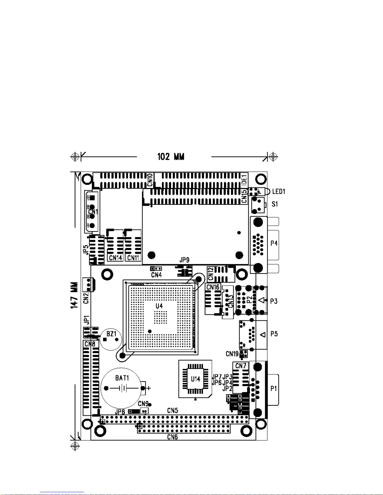
2.1 BOARD LAYOUT & DIMENSIONS.................................................................7
2.2 UNPACKING PRECAUTIONS .......................................................................8
2.3 COMPACT FLASH SETTINGS (JP1) ..............................................................8
2.4 COM2 MODE SETTINGS (JP2, JP3, JP4, JP6)..............................................9
2.5 COM2 PIN 8 RI SETTINGS (JP7)..............................................................9
2.6 EXTERNAL SWITCHES AND INDICATORS (JP5) ................................................9
2.7 CLEAR CMOS SETUP (JP8)...................................................................10
2.8 TFT LCD SETTINGS (JP9).................................................................... 10
CHAPTER 3 CONNECTORS......................................................................11
3.1 VGA CONNECTOR (P4)........................................................................11
3.2 SO-DIMM SOCKET CONNECTOR (CN3) .................................................... 12
3.3 LCD PANEL CONNECTOR 2.0MM 50 PIN (CN15)..........................................13
3.4 I2C CONNECTION (CN4)......................................................................13
3.5 PC/104 CONNECTION BUS (CN5, CN6)...................................................14
3.6 PARALLEL PORT CONNECTOR (CN10)........................................................ 15
3.7 SERIAL PORT CONNECTORS (CN7, 11, 14)................................................15
3.8 USB PORT CONNECTOR (CN12) ............................................................. 16
3.9 DIO PORT CONNECTOR (CN16) ............................................................. 16
3.10 LAN LED CONNECTOR (CN19) ............................................................17
3.11 EXTERNAL KEYBOARD CONNECTOR (CN13) ............................................... 17
3.12 FLOPPY DISK DRIVE CONNECTOR (CN8) ..................................................18
3.13 EXTERNAL POWER CONNECTOR (CN1)..................................................... 18
3.14 12V OR 5V CONNECTOR (CN2)............................................................19
3.15 EXTERNAL BATTERY CONNECTOR (CN9) ...................................................19
3.16 IDE DISK DRIVE CONNECTOR (IDE1)..................................................... 19
3.17 COMPACT FLASH CARD CONNECTOR (CF1)................................................20
CHAPTER 4 AWARD BIOS SETUP ...........................................................21
4.1 GETTING STARTED ..............................................................................21
4.2 MAIN MENU...................................................................................... 22

3
4.3 STANDARD CMOS FEATURES .................................................................24
4.4 ADVANCED BIOS FEATURES...................................................................27
4.5 ADVANCED CHIPSET FEATURES................................................................ 30
4.6 INTEGRATED PERIPHERALS.....................................................................30
4.7 POWER MANAGEMENT SETUP ..................................................................32
4.8 PNP/PCI CONFIGURATIONS ...................................................................34
4.9 LOAD FAIL-SAFE DEFAULTS....................................................................36
4.10 LOAD OPTIMIZED DEFAULTS .................................................................37
4.11 SET PASSWORD ...............................................................................37
4.12 SAVE & EXIT SETUP ..........................................................................39
4.13 EXIT WITHOUT SAVING.......................................................................40
APPENDIX A. WATCHDOG TIMER...........................................................41
APPENDIX B: THE E2 KEY™ FUNCTION..................................................43
APPENDIX C I/O INFORMATION ...........................................................44

4
Chapter 1 Introduction
Thank you for choosing the WAFER-4826EV SERIES STPC-DX2 133 CPU Board.
The WAFER-4826EV SERIES Board (denoted as WAFER-4826EV in other parts of
the manual) is an all-in-one CPU board with PC/104 for space-limited applications.
It provides all the functionalities of a full-fledged computer.
In addition, the WAFER-4826EV provides a VGA & LCD display controller on board,
which can support CRT/LCD resolutions up to 1024x768@64K colors.
This board has a built-in Compact Flash Interface for embedded applications. The
CF is a 100% software compatible hard disk. Users can use any DOS command
without any additional software utilities.

5
1.1 Specifications
CPU Embedded SGS Thomson STPC-DX2 133
System bus connector PC/104 connector
System memory Onboard SDRAM or one SO-DIMM socket, supports up to
128MB SDRAM
Enhanced IDE Supports one EIDE devices with BIOS auto-detection
capabilities
Floppy disk drive
interface Supports up to two floppy disk drives
Serial ports Four RS-232 ports with 16C550 UART (or compatible) with
16-byte FIFO buffer. Support up to 115.2Kbps. Ports can
be independently configured as COM1 or COM2.
Bi-directional parallel
port Configurable to LPT1, LPT2, LPT3 or disabled. Supports
EPP/ECP/SPP.
IrDA port Supports Infrared (IrDA) interface (Reserved/optional)
Watch-dog timer Can be set by 1-255 seconds intervals. Reset is triggered
when CPU does not periodically trigger the timer.
VGA display interface Complete backward compatibility to VGA and SVGA,
supports resolution up to 1024 x 768 @ 64K colors.
CF Interface One CF card with BIOS auto-detection capabilities.
Keyboard / Mouse
connector Supports standard PC/AT keyboards and PS/2 mice
Power consumption +5V @ 2.6A
Operating temperature 0°- 60°C (CPU requires a fan to use in environments
above 60°C)

6
1.2 Package Contents
The WAFER-4826EV package includes the following items:
WAFER-4826EV CPU board
1 Driver/Software CD
3 RS-2323 cables
1 Printer Cable
1 FDD cable
1 HDD cable
One 6-pin head which converts to two 6-pin DIN cable for keyboard and
mouse connection (Y Cable) x 1
User Manual
If any of these items is missing or damaged, please contact the dealer where the
product was purchased. Keep the shipping materials and carton in case you want
to ship or store the product in the future.

7
Chapter 2 Installation
This chapter describes how to install the WAFER-4826EV. Read the unpacking
information carefully and refer to the layout diagram of WAFER-4826EV below
whenever necessary.
2.1 Board Layout & Dimensions

8
2.2 Unpacking Precautions
Some components on WAFER-4826EV SBC are very sensitive to static and can be
damaged by a sudden power surge. To protect it from unintentional damage,
please be sure to follow these precautions:
Ground yourself to remove any static charge before touching WAFER-4826EV
SBC. You can do it by using an anti-static wrist strap connected to the
ground or by frequently touching any grounded conducting materials.
Handle your WAFER-4826EV SBC by its edges. Do not touch IC chips, leads
or circuitry as far as possible.
Do not plug in any connectors or set any jumpers when the power is on.
2.3 Compact Flash Mode Setting (JP1)
The Compact Flash on the WAFER-4826EV is Type II, and it uses IDE2.
JP1: Master/Slave Mode Settings
2 4 6
1 3 5
JP1 (1-2) DESCRIPTION
SHORT MASTER
OPEN SLAVE

9
2.4 COM2 Mode setting (JP2, JP3, JP4, JP6)
JP2, JP3, JP4, JP6: COM2 RS-232 or RS-422/485 Mode Selections
JP3
2 4 6
1 3 5
JP4
2 4 6
1 3 5
JP2
1 2 3
JP6
2 4
1 3
JP2 JP3 & JP4 DESCRIPTION
1-2 short 1-3 & 2-4 short RS-422/485
2-3 short * 3-5 & 4-6 short RS-232
JP6 DESCRIPTION
OPEN RS-422
1-3 & 2-4 short * RS-485
Note: If using RS422/485, the COM2 on the main board will be disabled.
2.5 COM2 Pin 8 RI Settings (JP7)
JP7: Pin 8 RI Settings
JP7
2 4 6
1 3 5
JP7 CN7 PIN 8
3-5, 4-6 Short * RI
3-5, 2-4 Short +5V
1-3, 2-4 Short +12V
2.6 External Switches and Indicators (JP5)
There are several external switches and indicators for monitoring and controlling
your CPU board. All functions are contained in the JP5 connector.

10
JP5: Pin Assignment and Functions
15 ..
..
5
3
1
16 ..
..
6
4
2
FUNCTION PIN DESCRIPTION
1 Battery +Ext. Battery 3 GND
5 GNDRESET 7 RESET
9 +5VHDD LED 11 IDE_LED -
13 Buzzer -SPEAKER 15 SPK SIGNAL
Jump
for
Buzzer
2 +5V
4 Rev. (FIR-RX)
6 IR-RX
8 GND
10 IR-TX
Reserved
(IrDA port)
12 CIR-RX
14 Rev. (KEYLOCK)Reserved
(KEYLOCK) 16 GND
2.7 Clear CMOS Setup (JP8)
If you want to clear the CMOS, for example, you forgot the your password, you
should clear the CMOS and reset the password, you should short JP8 (1-2) for
about 3 seconds. The password will be cleared from the CMOS.
JP8: Clear CMOS Setup (Reserved Function)
1 2 3
JP8 DESCRIPTION
2-3 NORMAL
1-2 CLEAR CMOS
2.8 TFT LCD Settings (JP9)
JP9: TFT LCD type (5V / 3V & FPCLK / #FPCLK) Settings
2 4 6
1 3 5
JP9 DESCRIPTION
2 – 4 5V TFT LCD
4 – 6 3V TFT LCD
1 – 3 #FPCLK
3 – 5 FPCLK

11
Chapter 3 Connectors
This chapter describes how to connect peripherals, switches and indicators to the
WAFER-4826EV board.
Table of Connectors
LABEL FUNCTION
P1 COM1 Connector
P2 External USB Connector (rev)
P3 PS/2 Mouse and Keyboard Connector
P4 VGA Connector
P5 Ethernet Connector
CN1 External Power Connector
CN2 12V or 5V(rev) Connector (for FAN etc.)
CN3 SO-DIMM Socket Connector
CN4 I2C Connector (rev)
CN5 PC/104-64 CON A
CN6 PC/104-40 CON B
CN7 COM2 Connector (RS-232/422/485)
CN8 Floppy Disk Drive Connector
CN9 External Battery Connector
CN10 Parallel Port Connector
CN11 COM3 Connector
CN12 USB Connector
CN13 External Keyboard Connector
CN14 COM4 Connector
CN15 LCD Panel Connector
CN16 DIO Connector
CN17 COM5 Connector
CN18 COM6 Connector
CN19 LAN LED Connector
IDE1 IDE Disk Drive Connector
CF1 Compact Flash Card Connector
3.1 VGA Connector (P4)
The built-in DB15 VGA connector of WAFER-4826EV can be directly connected to
your CRT monitor via the attached VGA cable.
P4: DB15 VGA Connector
PIN DESCRIPTION PIN DESCRIPTION
1 RED 2 GREEN
3 BLUE 4 NC
5 GROUND 6 GROUND
7 GROUND 8 GROUND
9 5V 10 GROUND
11 NC 12 SDA
13 HSYNC 14 VSYNC
15 SCL

12
3.2 SO-DIMM Socket Connector (CN3)
PIN DES. PIN DES. PIN DES. PIN DES.
1 GND 19 MD7 37 MD8 55 GND
2 GND 20 MD39 38 MD40 56 GND
3 MD0 21 GND 39 MD9 57 NC
4 MD32 22 GND 40 MD41 58 NC
5 MD1 23 DQ0 41 MD10 59 NC
6 MD33 24 DQ4 42 MD42 60 NC
7 MD2 25 DQ1 43 MD11 61 CLK0
8 MD34 26 DQ5 44 MD43 62 CKE0
9 MD3 27 3.3V 45 3.3V 63 3.3V
10 MD35 28 3.3V 46 3.3V 64 3.3V
11 3.3V 29 MA0 47 MD12 65 RAS#
12 3.3V 30 MA3 48 MD44 66 CAS#
13 MD4 31 MA1 49 MD13 67 WE#
14 MD36 32 MA4 50 MD45 68 CKE1
15 MD5 33 MA2 51 MD14 69 CSA#
16 MD37 34 MA5 52 MD46 70 NC
17 MD6 35 GND 53 MD15 71 CSB#
18 MD38 36 GND 54 MD47 72 NC
PIN DES. PIN DES. PIN DES. PIN DES.
73 GND 91 GND 109 MA9 127 MD27
74 CLK1 92 GND 110 BA1 128 MD59
75 GND 93 MD20 111 MA10 129 3.3V
76 GND 94 MD52 112 MA11 130 3.3V
77 NC 95 MD21 113 3.3V 131 MD28
78 NC 96 MD53 114 3.3V 132 MD60
79 NC 97 MD22 115 DQ2 133 MD29
80 NC 98 MD54 116 DQ6 134 MD61
81 3.3V 99 MD23 117 DQ3 135 MD30
82 3.3V 100 MD55 118 DQ7 136 MD62
83 MD16 101 3.3V 119 GND 137 MD31
84 MD48 102 3.3V 120 GND 138 MD63
85 MD17 103 MA6 121 MD24 139 GND
86 MD49 104 MA7 122 MD56 140 GND
87 MD18 105 MA8 123 MD25 141 SDA
88 MD50 106 BA0 124 MD57 142 SCL
89 MD19 107 GND 125 MD26 143 3.3V
90 MD51 108 GND 126 MD58 144 3.3V

13
3.3 LCD Panel Connector 2.0mm 50Pin (CN15)
2 50
.. ..
.
.. ..
1 49
PIN DESCRIPTION PIN DESCRIPTION
1 NC 2 NC
3 NC 4 NC
5 NC 6 NC
7 NC 8 NC
9 NC 10 NC
11 NC 12 NC
13 NC 14 FPD_R3
15 FPD_R5 16 FPD_R4
17 NC 18 FPD_R2
19 NC 20 FPD_R0
21 FPD_R1 22 FPD_G4
23 FPD_G3 24 FPD_G2
25 FPD_G5 26 FPD_G1
27 FPD_B5 28 FPD_G0
29 +LCD 30 +LCD
31 NC 32 NC
33 FPD_B2 34 FPD_B4
35 FPD_B1 36 FPD_B3
37 FPD_B0 38 NC
39 FPD_EN 40 NC
41 FPD_CK 42 EN_BKL
43 EN_VDD 44 FPD_VS
45 EN_VEE 46 FPD_HS
47 GND 48 GND
49 +VBL 50 +VBL
3.4 I2C Connection (CN4)
1 2 3
CN4 DESCRIPTION
1 DATA
2 CLOCK
3 GND

14
3.5 PC/104 Connection Bus (CN5, CN6)
The WAFER-4826EV's PC/104 expansion bus lets you attach any PC/104 module.
There are two PC/104 connectors on this board: PC/104-64 and PC/104-40.
CN5: PC/104-64 CON A 64
2
1
1
2
CN6: PC/104-64 CON B 40
CN5: PC/104-64 CON A
PIN DES. PIN
DES.
1 IOCHCK# 2 GND
3 SD7 4 RSTDRV
5 SD6 6 +5V
7 SD5 8 IRQ9
9 SD4 10 -5V
11 SD3 12 DRQ2
CN6: PC/104-64 CON B 13 SD2 14 -12V
PIN
DES. PIN DES. 15 SD1 16 ZWS
2 GND 1 GND 17 SD0 18 +12V
4 MCS16 3 SBHE# 19 IOCHRDY 20 GND
6 IOCS16 5 LA23 21 AEN 22 SMEMW#
8 IRQ10 7 LA22 23 LA19 24 SMEMR#
10 IRQ11 9 LA21 25 LA18 26 IOW#
12 IRQ12 11 LA20 27 LA17 28 IOR#
14 IRQ15 13 LA19 29 SA16 30 DACK3#
16 IRQ14 15 LA18 31 SA15 32 DRQ3
18 DACK0# 17 LA17 33 SA14 34 DACK1#
20 DRQ0 19 MEMR# 35 SA13 36 DRQ1
22 DACK5# 21 MEMW# 37 SA12 38 REFRESH#
24 DRQ5 23 SD8 39 SA11 40 SYSCLK
26 DACK6# 25 SD9 41 SA10 42 IRQ7
28 DRQ6 27 SD10 43 SA9 44 IRQ6
30 DACK7# 29 SD11 45 SA8 46 IRQ5
32 DRQ7 31 SD12 47 SA7 48 IRQ4
34 +5V 33 SD13 49 SA6 50 IRQ3
36 MASTER# 35 SD14 51 SA5 52 DACK2
38 GND 37 SD15 53 SA4 54 TC
40 GND 39 NC 55 SA3 56 ALE
57 SA2 58 +5V
59 SA1 60 OSC
61 SA0 62 GND
63 GND 64 GND

15
3.6 Parallel Port Connector (CN10)
This port is usually connected to a printer. WAFER-4826EV includes an on-board
parallel port to be accessed through a 26-pin mini-pitched flat-cable connector
CN10.
CN10: 26-PIN Female Connector
12
STB#
AFD#
DATA 0
ERROR#
DATA 1
INIT#
DATA 2
SLIN#
DATA 3
GND
DATA 4
GND
DATA 5
GND
DATA 6
GND
DATA 7
GND
ACK#
GND
BUSY
GND
PE
GND
SLCT#
NC
25
26
3.7 Serial Port Connectors (CN7, CN11, CN14)
The WAFER-4826EV offers two high-speed NS16C550 compatible 16-byte serial
Read/Receive UART FIFO ports.
CN11, CN14: (COM3, COM4) 10-PIN Female Connector
12
DCD# DSR#
RXD
RTS#
TXD
CTS#
DTR#
RI#
GND NC
9
10
CN7: (COM2) 10-PIN Female Connector
2 10
1 9
PIN DESCRIPTION PIN DESCRIPTION
1 TX- / DCD# 2 DSR#
3 TX+ / RXD 4 RTS#
5 RX+ / TXD 6 CTS#
7 RX- / DTR# 8 RI#/5V/12V
9 GND 10 NC

16
3.8 USB Port Connector (CN12)
2 8
1 7
CN12 DESCRIPTION
1 +5V
2 GND
3 P0D-
4 P1D+
5 P0D+
6 P1D-
7 GND
8 +5V
3.9 DIO Port Connector (CN16)
This port is connected to DIO 0 to 7; all pins can be set as input or output.
IO port DESCRIPTION
320 (hex) Direction Register
DIO 0 (bit0) ~ DIO 7 (bit7)
1=input; 0=Output
326 (hex) DIO Port
DIO 0 (bit0) ~ DIO 7 (bit7)
2 10
1 9
CN16 DESCRIPTION
1 GND
2 +5V
3 DIO 7
4 DIO 6
5 DIO 5
6 DIO 4
7 DIO 3
8 DIO 2
9 DIO 1
10 DIO 0

17
3.10 LAN LED Connector (CN19)
2 4
1 3
CN19 DESCRIPTION
1 LINK-
2 LINK+
3 ACT-
4 ACT+
3.11 External Keyboard Connector (CN13)
The included 5 or 6-pin plug will convert to two 6-pin DIN cables for keyboard
(mouse) connection enables users to connect PS/2 keyboard (and mouse).
Simply connect your keyboards and mice to the attached cable to use them as
you normally would.
CN13 : PS/2 Keyboard (mouse/rev) Connector
6 1
CN13 DESCRIPTION
1 KEYBOARD CLOCK
2 KEYBOARD DATA
3 NC. (Rev. MOUSE CLOCK)
4 GND
5 SV
6 NC. (Rev. MOUSE DATA)

18
3.12 Floppy Disk Drive Connector (CN8)
The WAFER-4826EV board is equipped with a 34-pin daisy-chain drive connector
cable which supports up to two floppy drives. The detailed pin assignments of the
connector is described as below:
2 34
1 33
PIN DESCRIPTION PIN DESCRIPTION
1 GND 2 REDUCE WRITE
3 GND 4 NC
5 GND 6 NC
7 NC 8 INDEX#
9 GND 10 MOTOR ENABLE A#
11 GND 12 DRIVE SELECT B#
13 NC 14 DRIVE SELECT A#
15 GND 16 MOTOR ENABLE B#
17 GND 18 DIRECTION#
19 GND 20 STEP#
21 GND 22 WRITE DATA#
23 GND 24 WRITE GATE#
25 GND 26 TRACK 0#
27 GND 28 WRITE PROTECT#
29 NC 30 READ DATA#
31 GND 32 SIDE 1 SELECT#
33 NC 34 DISK CHANGE#
3.13 External Power Connector (CN1)
The WAFER-4826EV has an on-board external power connector CN1. The
WAFER-4826EV is only powered by VCC (5V), which is conducted through pin 4 of
the external power connector CN1, and power GND from pin 2 and pin 3. The
extra power supply +12V provided by CN1 will be passed to CN5 and CN6 for
PC104 slot use only.
CN1: External Power Connector
1 2 3 4
PIN DESCRIPTION
1 +12V
2 GND
3 GND
4 +5V

19
3.14 12V or 5V Connector (CN2)
The WAFER-4826EV provides an optional fan power connector, which works only
when +12V power is supplied to CN1. Please note that a heat sink has already
been installed in STPC chip of the WAFER-4826EV. However, when running
WAFER-4826EV under a temperature of above 60℃, users will have to add an
additional CPU cooling fan.
CN2: 12V or 5V for FAN etc. connector
1GND
2
+12V
3
NC(+5V)
3.15 External Battery Connector (CN9)
The WAFER-4826EV provides an (Molex 1.25mm 2pin) optional battery connector.
Note: If external battery is to be used, please remove the on board battery.
1 Battery +
2 GND
3.16 IDE Disk Drive Connector (IDE 1)
You can attach four IDE (Integrated Device Electronics) hard disk drives to the
WAFER-4826EV IDE controller.
IDE1: HDD Connector
1 2
RESET# GND
DATA 7 DATA 8
DATA 6 DATA 9
DATA 5 DATA 10
DATA 4 DATA 11
DATA 3 DATA 12
DATA 2 DATA 13
DATA 1 DATA 14
DATA 0 DATA 15
GND
NC
DREQ
GND
IOW#
GND
IOR#
GND
IORDY GND
IDACK# GND
IDE
INTERRUPT NC
SA1 NC
SA0 SA2
CS0# CS1#
IDE ACTIVE# GND
+5V +5V
GND NC
43
44
Table of contents
Popular Control Unit manuals by other brands

Bandini Industrie
Bandini Industrie GI.BI.DI. DSC80 Instructions for installations

National Instruments
National Instruments PXI-6683 Series installation guide

Runxin
Runxin 51215 instruction manual

MR
MR CEDASPE DAROC EDS-R Series operating instructions

Haas
Haas PCOOL Installation

Maretron
Maretron SMS100 user manual