Intel GIGA GD16556 User manual

General Description
The GD16556 and GD16557 constitute a
high performance multi-bitrate tran-
sponder chip set designed for Optical
Network applications. The devices are
available with either LVDS or LVPECL
low-speed I/Os.
The chip set is compatible with the line
rates:
uSDH STM-1 / SONET OC3
uSDH STM-4 / SONET OC12
uSDH STM-16 / SONET OC48
uGigabit Ethernet
Switching between the bit rates is possi-
ble on-the-fly through select pins.
The chip set is designed for interconnect-
ing the high-speed line interface to stan-
dard CMOS ASICs or FPGAs. The
on-chip VCO and PLL blocks eliminate
external high-speed clock signals and
complicated timing relations.
Digital “Wrapping” Modes
GD16556 and GD16557 are capable of
transmitting and receiving data at in-
creased rates if overhead is needed for
system level service purposes. The de-
vices can operate with STM-1 (OC3),
STM-4 (OC12), STM-16 (OC48) and
Gigabit Ethernet line rates multiplied by a
fraction. Fractions available are 32/31,
16/15 and 15/14. Thus, for example, data
might be transmitted (or received) at a
rate of 32/31 times 2.488 Gbit/s with a
high- speed clock of 2.568 GHz. The
fractions are available through selection
of programmable dividers.
Signal Levels and Power Supply
Low speed interfaces are LVDS/LVPECL
compatible. The high-speed output from
the transmitter GD16557 is of CML-type
(open collector). Select pins are LVTTL
compatible.
Low power consumption is achieved by a
single +3.3 V power supply and by omit-
ting all circuitry, which can easily be im-
plemented in the low speed system
ASIC.
The devices are housed in 100 pin TQFP
EDQUAD thermal enhanced packages.
an Intel company
Data Sheet Rev.: 23
Preliminary
Features
General
lSDH (SONET) STM-1(OC3) /
STM-4(OC12) / STM-16(OC48) / GE
compatible
lTrue on-the-fly multi-bit rate operation
lBypass for non-compatible bit rates
lLoop-back for system test mode
lOverhead data rate capability
–15/14 (7% overhead)
–16/15 (6% overhead)
–32/31 (3% overhead)
lLVDS/LVPECL low-speed I/O
lSingle power supply: +3.3 V
l100 pin TQFP EDQUAD packages
GD16556 (Receiver)
lClock and Data Recovery
l1:16 Demultiplexer
lDifferential input with 5 mVPP
sensitivity
lLoss of signal monitor
lBit consecutive monitor
lLock detect monitor
lPower dissipation: 1.3 W (typ.)
GD16557 (Transmitter)
l16:1 Multiplexer
lOptional double PLL jitter-clean up
lCounter or forward clocked
low-speed interface
lPLL lock-detect
lPower dissipation: 1.3 W (typ.)
Applications
lDigital “Wrappers”
lOptical Networking
lTransponders
lSDH/SONET FEC out-of-band
systems
lNetwork interconnects
lGateways
lDatacom
*: Patent pending
2.5 Gbit/s
Transponder
Chip Set with
Digital “Wrapping”
GD16556/GD16557*
Clock
Clock
Clock
Clock
VCXO
VCXO
Clock
Clock
Clock
Clock
16
16
16
16
System
ASIC
System
ASIC
Line
Side
System
Side
GD16556
CDR &
DeMUX 1:16
GD16556
CDR &
DeMUX 1:16
GD16557
Jitter
Cleaner &
MUX 16:1
GD16557
Jitter
Cleaner &
MUX 16:1
STM-1 / OC3
STM-4 / OC12
STM-16 / OC48
Gigabit
Ethernet
STM-1 / OC3
STM-4 / OC12
STM-16 / OC48
Gigabit
Ethernet
STM-1/OC3
STM-4/OC12
STM-16/OC48
Gigabit
Ethernet
STM-1/OC3
STM-4/OC12
STM-16/OC48
Gigabit
Ethernet
Times:
1,
15/14,
16/15,
32/31
Times:
1,
16/15,
32/31
15/14,

Functional Details
General
The transmitter and receiver chip set is
optimised for transponder solutions and
Optical Network interconnects such as
bridges and gateways. The intended
transponder system is shown on page 1.
Transponder System Jitter
Specifications
The transponder system exceeds ITU-T
(recommendation G.825 for a Type B
regenerator) and Bellcore recommenda-
tions with respect to output jitter.
The jitter-tolerance on the input side ex-
ceeds ITU-T (recommendation G.958)
and Bellcore recommendations.
GD16556 - The Receiver
The GD16556 receiver integrates:
ua Limiting Input Amplifier (LIA)
ua Bang-Bang Phase Detector
ua Phase Frequency Detector
ua Voltage Controlled Oscillator
into a complete Clock Data Recovery
(CDR) system. The CDR is followed by a
1:16 de-multiplexer. A lock-detect output
monitors if the CDR is locked onto the re-
ceived serial data.
GD16557 - The Transmitter
The GD16557 transmitter is a 16:1 multi-
plexer with an integrated double PLL to-
pology requiring an external VCXO to
achieve a superior jitter clean-up.
System Speed
The pins RSEL1 and RSEL2 choose the
line rate (155 Mbit/s, 622 Mbit/s,
2.488 Gbit/s and 1.250 Gbit/s). It is the
responsibility of the system to monitor
the bit rate and assert the signals RSEL1
and RSEL2.
Bypass Data Path
To enable handling of non-compatible bit
rates a bypass data path is featured. This
path bypasses the CDR in the receiver
and the multiplexer in the transmitter.
The bypass data I/O (BP, BPN) are CML
compatible with a LVTTL compatible ac-
tive low enable pin BPEN in order to re-
duce noise at the printed circuit board
when disabled. The system needs to
monitor the incoming bit rate and assert
the BPEN signal properly.
Figure 1. An example configuration of a channel in a transponder system
Figure 2. The core circuit
Figure 3. Basic PLL frequency syntesis
Loop-back Data and Clock
Path
A loop-back data path is featured to en-
able easy means of fault diagnostics and
system verification etc. The loop-back
data and clock path bypasses the de-
multiplexer in the receiver and the multi-
plexer in the transmitter. The loop-back
data I/O is named LB, LBN and the
loop-back clock I/O is named LBCK,
LBCKN. To enable the loop-back paththe
system needs to assert the signal LBEN.
The Transponder System
The chip set is designed for the tran-
sponder system shown on the front page.
The system consists of a receiver
GD16556, a system ASIC tailored for the
application and a transmitter GD16557.
Such a three-device configuration is
needed for each direction.
Appropriate timing relations are assured
by the PLL topology of the system. Fur-
thermore, the choice of PLL topology as-
Data Sheet Rev.: 23 GD16556/GD16557* Page 2 of 28
32/31 155.50 MHz 155.50 MHz
DO0/N DO/N
DO15/N CKO/N
CKO/N
DI/N
DI0/N
DI15/N
CNTCK/N
FCK/N
XCK1/N
CKI/N
RECCK/N
CKREF/N
40.134 MHz
40.134 MHz
VCXO
40.134 MHz
Data Data
16 16
System
ASIC
GD16556 GD16557
32/31
2.488 Gbit/s
2.488 Gbit/s
2.488 GHz
GD16557 Transmitter
GD16556 Receiver
Bang-Bang
Phase
Detector
Phase
Frequency
Detector
VCO
VCO
VCXO
Phase
Frequency
Detector
/M
Frequency
Divider
/N
Frequency
Divider
High-speed
Data
Reference
Clock
VCO
Phase
Frequency
Detector
Frequency
Divider
/N
F
M
STANDARD
Referency
Frequency

sures that the transponder system meets
the jitter specifications.
The core circuit is illustrated on Figure 2
For simplicity the system ASIC and con-
nections to this device have been omit-
ted. Also, the PLLs have been somewhat
simplified omitting the charge pumps and
loop-filters.
Referring to Figure 2 the functionality of
the system is as follows; looking at the
CDR device GD16556 the incoming high-
speed data signal is sampled by the
bang-bang detector. The bang-bang de-
tector outputs a signal that drives a
charge pump and hence controls the
on-chip VCO in the CDR. This causes
the VCO frequency to match the data fre-
quency. A reference frequency for the
CDR is supplied from the VCXO located
on the transmit side. The reference fre-
quency assures that the VCO frequency
does not deviate too much from the (ex-
pected) bit rate. Since the CDR in the re-
ceiver needs to be within 500 ppm of the
bit rate, the VCXO frequency should not
deviate more than 200 ppm (TBD) from
its proper centre frequency under any
conditions. Please refer to the section on
the GD16556 device on page 5 forade
-
tailed discussion of the CDR functional-
ity. Valid VCXO centre frequencies are
outlined on Table 1 on page 11.
Turning to the transmit device GD16557
the device implements a double PLL to-
pology. The double PLL is required to
make the system exceed the ITU-T /
Bellcore jitter recommendations inde-
pendent of the bit rate. On the CDR side
a trade-off exists between jitter-tolerance
and jitter-transfer. It is difficult to achieve
a proper jitter-tolerance and simulta-
neously a proper jitter-transfer no matter
the bit rate not having the possibility to
modify the loop-filter. However, by imple-
menting a PLL with a low bandwidth (typ.
less than 10 kHz) it is possible to equal-
ize penalty in jitter- transfer. The result is
an excellent jitter- tolerance no matter
the bit rate. The drawback of this solution
is the need for a high-Q oscillator. Since
it is not possible to realise a high-Q
on-chip oscillator the high-Q oscillator is
added as an external crystal type VCO
(VCXO). Figure 2 shows the double PLL
implemented in the GD16557. The
VCXO is locked to the divided clock out-
put from the CDR device. Now, the trans-
mitter on-chip VCO is locked to the
VCXO in a second PLL. This causes the
VCO to track the VCXO achieving supe-
rior phase-noise properties of the
high-speed output data.
The transponder system allows for in-
creased bit rates. The use of increased
standard bit rates is commonly known as
“digital wrapping”. The chip set supports
digital wrapping by implementing pro-
grammable frequency dividers
(prescalers). By proper setting of the
dividers the transponder system will com-
ply with bit rates equal to a standard bit
rate ( STM-1 / OC3, STM-4 / OC12,
STM-16 / OC48, GE) multiplied by a frac-
tion larger than one. Supported fractions
are 15/14, 16/15 and 32/31.
Supporting digital wrapping corresponds
with an ability to tune the VCOs in the
CDR and transmit device onto the proper
frequency. Basic frequency synthesis is
applied to implement this functionality.
The principle is illustrated on Figure 3.By
choosing the frequency of the reference
clock signal as a standard bit rate fre-
quency (denoted fSTANDARD) divided by M,
the frequency of the VCO (denoted fVCO)
becomes:
ffN
M
VCO
STANDARD
=´
The on-chip frequency dividers imple-
ments divide by 56, 60, 62 and 64. Sig-
nals MSEL1 and MSEL2 choose the
divide ratio. It is the responsibility of the
system to configure the GD16556/
GD16557 with respect to the bit rate
(RSEL1, RSEL2) and the overhead frac-
tion factor (MSEL1, MSEL2). Table 1 on
page 11 outline the recommended VCXO
frequencies with respect to the settings
of RSEL1, RSEL2 and MSEL1, MSEL2.
Data Sheet Rev.: 23 GD16556/GD16557* Page 3 of 28

Practical Considerations
The PCB Layout
The PCB must be designed with shortest
possible conductors for the data inter-
faces and clock distribution. Design
these connections as transmission lines.
The LVTTL compatible select pins are
supplied with an on-chip pull-up resistor
(Figure 4) given a default “1" when not
connected.
The LVDS connection scheme is shown
on Figure 5. The LVDS I/Os have an
impendance of 100 Wand do not require
external termination resistors.
LVPECL connection schemes are shown
on Figures 6 and 7.
The high-speed CML type input buffers
are supplied with on-chip termination re-
sistors as shown on Figure 9.
The heatsink on the TQFP EDQUAD
package should be connected to a VEE
power supply plane on the PCB with ca-
pability to carry away the dissipated heat.
Noise Considerations
When designing the PCB utmost impor-
tance should be put on noise isolation.
De-coupling capacitors should be applied
to each supply pin. Care should be taken
to reduce ground bounces. Be aware
that any noise added to the VCXO output
signal translates directly into jitter on the
high-speed output clock. Hence, the
VCXO(s) should be differential and lo-
cated close to the transmit device.
Figure 4. LVTTL pull-up resistor
Figure 5. LVDS connection
Figure 6. LVPECL output termination, AC-coupled.
Figure 7. LVPECL output termination, DC-coupled.
Figure 8. CML output buffer Figure 9. CML input buffer
Data Sheet Rev.: 23 GD16556/GD16557* Page 4 of 28
VEE
VDD
LVTTL
16kW
50W
50W
LVDS
Output Input
LVDS
180W50W
180W
100nF
100nF
0V
(VEE)
2V
(VDD -1.3V)
50W
LVPECL
Output Input
LVPECL
150W
150W
150W
VEE
VEE
LVPECL
Output Input
LVPECL
2x
50W
50 LineW
2x
50W
VDD
20mA
CML
VDD
2×
50W
Positive
Input
Termination
Negative
Input

The Receiver – GD16556
General
The GD16556 is an on-the-fly program-
mable multi-bitrate CDR and 1:16 de-
multiplexer with emphasis put on tran-
sponder applications. The device is ca-
pable of demultiplexing a serial bit
stream at 155 Mbit/s, 622 Mbit/s,
1.250 Gbit/s or 2.488 Mbit/s into 16 par-
allel low speed channels.
When operated in non-transponder appli-
cations the device meets all ITU-T /
Bellcore jitter specifications when used
with the recommended loop filter (Refer
to Figure 19). Note that the loop-filter is
dependent on the bit-rate in order to
achieve the jitter specifications. In this
case true on-the-fly multi-bitrate opera-
tion is not an option.
When operated in the transponder con-
figuration Figure 1 true multi-bitrate oper-
ation is made possible by a trade-off
between jitter-tolerance and jitter-transfer
in the receiver. By allowing an increase
in jitter-transfer the jitter tolerance is
achieved at any bitrate. The double-PLL
jitter clean-up system on the transmitter
“equalizes”this penalty on the transmit
side.
Figure 10.GD16556 - Block diagram
Hence, the overall transponder system
will be well within the jitter specifications.
Select pins are LVTTL compatible. The
LVTTL inputs are internally pulled high
by default.
The device operates from a single 3.3 V
positive power-supply and the consump-
tion is 1.3 W (typ.).
Digital “Wrapping”Modes
The GD16556 is capable of receiving
data at increased bit rates if overhead
capability for system purposes is needed.
Table 1 on page 11 outlines the con-
straints on the reference clock and the
setting of the MSEL1, MSEL2 signals for
the transponder system shown on Figure
1.
Clock Generator Circuit
The clock generator circuit in the
GD16556 contains two independent di-
viders.
One divider (divide by 1 for STM-16/OC
48, divide by 2 for Gigabit Ethernet, di-
vide by 4 for STM-4/OC 12 and divide by
16 for STM-1/OC 3) generates the line
rate clock to the Bang-Bang phase de-
tector plus decision sampling gaate.
A second divider (56, 60, 62 and 64) di-
vides the VCO frequency to generate a
signal that is compared with the refer-
ence clock in the Phase Frequency De-
tector (PFD). This signal is also
forwarded to the transmitter GD16557
when operated in a transponder system.
The circuit topology allows for a straight-
forward increase in line rates by a frac-
tion. The simplest illustration is by
example.
Data Sheet Rev.: 23 GD16556/GD16557* Page 5 of 28
DI
DIREF
BP
LB
LBCK
CDRSEL
BPN
LBN
LBCKN
BPEN
LBEN
CKRSEL
CKREFA
CKREFB
DIN
DIREFN
RSEL1..2
VCTL
MSEL1..2
CKREFAN
CKREFBN
DO0..15
FCK
CKO
DO0N..15N
LOCK
OUCHP
VDDL
VDDO
VDDP
VDDV
VDD
VEEL
VEEP
VEEV
VEE
FCKN
CKON
DeMUX
1:16
Bang
Bang
Phase
Detect.
LIA
Lock
Detect
Clock Generator
PFD CHAP
/1, /2
/4, /16
& &
&
/56, /60
/62, /64
2
2
4
4
16
F
Clock
V

Assume the incoming line rate equals
32/31 times 2.488 Gbit/s. Thus, the VCO
frequency should equal 2.568 GHz. The
reference clock input (CKREF, CKREFN)
is defined as 2.488 GHz/62 equal to
40.134 MHz. Now the VCO frequency is
divided by 64 and compared on the PFD.
This will cause the VCO to tune onto a
frequency of 64/62 that is 32/31 times
2.488 GHz due to the PLL feedback.
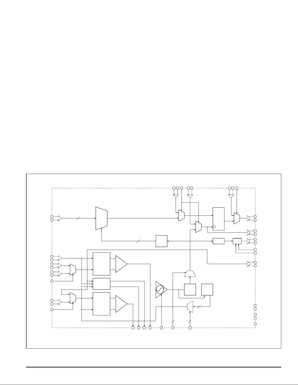
The topology of the circuit splits the line
rate generation from the fraction select
allowing any combination of the two.
For simplicity a third divider that gener-
ates clocks to the de-multiplexer is not
shown on the block diagram.
Lock Detect Circuit
The Lock Detect Circuit continuously
monitors the frequency difference be-
tween the reference clock and the di-
vided VCO clock. If the reference clock
and the divided VCO frequency differ by
more than 500 ppm it switches the PFD
into the PLL in order to pull the VCO
back inside the lock-in range. This mode
is called the acquisition mode.
The PFD is used to ensure predictable
lock up conditions for the GD16556 by
locking the VCO to an external reference
clock source. It is only used during acqui-
sition and pulls the VCO into the lock
range where the Bang-Bang Phase De-
tector is capable of acquiring lock to in-
coming data. The PFD is digital with true
Phase/Frequency detectability.
Once the VCO is inside the lock-range
the lock-detection circuit switches the
Bang-Bang phase detector into the PLL
in order to lock to the data signal. This
mode is called CDR mode.
Bang-Bang Phase Detector
The Bang-Bang Phase Detector is used
in CDR mode as a true digital type detec-
tor, producing a binary output. It samples
the incoming data twice each bit period:
once in the transition of the (previous) bit
period and once in the middle of the bit
period. When a transition occurs be-
tween 2 consecutive bits - the value of
the sample in the transition between the
bits will show whether the VCO clock
leads or lags the data. Hence the bit tran-
sition point controls the PLL, thereby en-
suring that data is sampled in the middle
of the eye, once the system is in CDR
mode. The external loop filter compo-
nents control the characteristics of the
PLL.
The binary output of either the PFD or
the Bang-Bang Phase Detector (depend-
ing of the mode of the lock-detection cir-
cuit) is fed to a Charge Pump capable to
sink/source current or tristate. The output
of the Charge Pump is filtered through
the Loop Filter and controls the tuning-
voltage of the VCO.
Figure 11.GD16556 - Loop filter
As a result of the continuous monitoring
Lock Detect Circuit the VCO frequency
never deviates more than 500 ppm from
the reference clock before the PLL is
considered to be ’Out of Lock’. Hence the
acquisition time is predictable and short
and the output clock (CKOUT) is always
kept within the 500 ppm limit, ensuring
safe clocking of down stream circuitry.
The LOCK Signal
The status of the lock-detection circuit is
given by the LOCK signal. In CDR mode
LOCK is steady high. In acquisition mode
LOCK is alternating indicating the contin-
uous shifts between the Bang-Bang De-
tector (high) and the PFD (low).
The BC_DET Signal
An internal circuit monitors input data
transitions and gives a BC_DET output
signal which is asserted if more than 256
consecutive identical bits, 0s or 1s, are
detected.
BC_DET will be de-asserted only after
approximately 16 bit transitions are de-
tected within a time period proportional to
the selected data rate (50 ns at STM 16 /
OC-48).
The LOCK_DET Signal
The LOCK_DET signal is a status output,
which monitors the status of the internal
lock detect circuit of the GD16556 CDR
logic and the output of the BC_DET cir-
cuit.
LOCK_DET is asserted (set HIGH) if the
VCO frequency differs from the reference
frequency by ±500 ppm. This ‘out of
lock’condition is detected by the internal
Lock Detect circuit described previously.
LOCK_DET is also asserted in the case
of the absence of data, which is detected
by the BC_DET circuit within the reaction
time of the internal PLL lock detect
system.
If data is absent, the divided VCO fre-
quency will drift away from the reference
frequency until they differ by ±500 ppm.
The internal Lock Detect logic will alter-
nate between CDR and acquisition mode
until data returns, enabling the GD16556
to acquire lock and function in CDR
mode.
The LOCK_DET signal, however, will re-
main asserted until BC_DET is de- as-
serted and the internal lock detect circuit
is operating in CDR mode.
The CDR circuitry of the GD16556 has
been fine-tuned to provide an accurate
stable clock output from the VCO when
data is present. Due to the precise nature
of the internal VCO, when data is absent
the clock output frequency will drift slowly
from the recovered clock frequency until
an out of lock condition is detected. The
time taken for the GD16556 to go ‘out of
lock’in the absence of data will typically
be at least 3 ms, unless an external cir-
cuit is used to pull the VCO frequency
away from the reference frequency.
When loss of data is detected, i.e.
BC_DET is asserted, or the divided VCO
frequency differs from the reference fre-
quency by ±500 ppm, LOCK_DET is as-
serted and the internal lock detect circuit
switches to acquisition mode. This will
give a stable output clock during a loss of
data condition.
When BC_DET is de-asserted and the
divided VCO frequency is within 500 ppm
of the reference frequency, LOCK_DET
will be de-asserted within 500 ms, inde-
pendent of selected data rate.
LOS_DET
The Loss Of Signal DETection
(LOS_DET) alarm output is low during
normal operation.
The LOS_DET signal is the output from a
digital Bit Error Flag (BEF) circuit which
monitors the number of false bit transi-
tions in the data signal. An internal flag is
raised if the number of false transitions is
above a predefined level, i.e. if the Bit
Error Rate (BER) is above the corre-
sponding BER level.
Data Sheet Rev.: 23 GD16556/GD16557* Page 6 of 28
CHAP
OUCHP
1Fm
24 W
VCTL
VDDV

This has been realised by counting the
false bit transitions. If this counter runs
out within a time period the BEF flag is
set. The length of the counter may be set
by external select signals (SBER0 and
SBER1). The time period that the false
errors are counted within is 64 kbit/s cor-
responding to 26 ms at STM 16 / OC-48
data rate. The length of the counter may
be set to detect approximate Bit Error
Rates of 0.5E-3, 1E-3, 2E-3 or 4E-3.
The input to the BEF circuit is derived
from Bang-Bang detector sample data.
As discussed above, the Bang-Bang de-
tector samples the incoming data twice
each bit period, once at the transition and
once in the middle of the eye. If the value
of the samples in the middle of the eye
for two consecutive bits is equal but the
value of the transition sample is different
then a bit error has occurred.
As the BEF system detects false bit tran-
sitions between two consecutive bits,
only bit errors due to high frequency
noise are detected. Therefore there will
not be a 1:1 correlation between the ac-
tual BER of the signal and the number of
errors detected by the BEF system. How-
ever the actual bit error rate is correlated
to the number of errors detected in the
BEF system. This means that by choos-
ing the appropriate counter length, it will
be possible for the BEF system to set the
BEF flag at a user selectable bit error
rate.
Once the LOS_DET signal has been as-
serted, it will be de-asserted only when
the BER is less than ¼of the set rate for
a period which is proportional to the se-
lected data rate. (at least 125 msat
STM16 / OC-48).
Data Input
The input amplifier (DI / DIN) is designed
as a Limiting Amplifier (LIA) with a sensi-
tivity better than 10 mV (differential).
The inputs may be either AC or DC cou-
pled. If the inputs are AC coupled the
amplifier features an internal offset can-
celling DC feedback. Notice that the off-
set cancellation will only work when the
input is differential and AC-coupled as
shown on Figure 12.
Bit Order
The serial data stream is output with the
first bit received on DO0, the second on
DO1 and the last bit in a 16 bit frame on
DO15.
Figure 12.AC coupled input (using internal offset compensation).
Figure 13.DC coupled input (ignoring internal offset compensation). VTT depends on
the termination requirements of the previous stage, and the resulting ampli-
tude on the input.
Data Sheet Rev.: 23 GD16556/GD16557* Page 7 of 28
DIREF
50R
From LINE
From LINE
VEE
VEE
50R
8k
8k
26dB
DIREFN
DIN
DI
+
-
DIREF
50R
From LINE
From LINE
VTT
VTT
50R
8k
8k
26dB
DIREFN
DIN
DI
+
-

The Transmitter – GD16557
General
The GD16557 is an on-the-fly program-
mable multi-bitrate multiplexer with em-
phasis put on transponder applications.
The device is capable of multiplexing
16 independent low speed channels into
one serial bit stream at 155 Mbit/s,
622 Mbit/s, 1.250 Gbit/s or 2.488 Mbit/s.
The device meets all ITU-T jitter require-
ments when used with the recommended
loop filter (refer to Figure 19).
The device can be either counter or for-
ward clocked.
Low-speed data and clock I/O are LVDS/
LVPECL compatible. The high-speed
outputs are open collectors (CML-type).
Select pins are LVTTL compatible. The
LVTTL inputs are internally pulled high
by default. The VCXO clock inputs are
LVPECL compatible.
The device operates from a single 3.3 V
positive power-supply and the consump-
tion is 1.3 W (typ.).
Figure 14.GD16557 - Block diagram
Digital “Wrapping”Modes
The fraction is chosen by the signals
MSEL1 and MSEL2. Table 1 on page 11
outlines the constraints on the bit rates
with respect to the VCXO frequencies.
Select signal settings are listed along.
The table is valid for the transponder sys-
tem shown on Figure 1.
Clock Generator Circuit
The Clock Generator circuit in the
GD16557 is much alike the one in the re-
ceiver GD16556. Please refer to the dis-
cussion in the section Clock Generator
Circuit in the GD16556 description.
Counter Clocking Scheme
When the GD16557 is used in tran-
sponder applications the input reference
clock to the transmitter (CKI, CKIN) is
generated by the receiver GD16556.
Please refer to Figure 10.
In non-transponder applications the
GD16557 may be operated with jitter
clean-up (including VCXO) or without
leaving the possibility to omit the VCXO.
If operation is desired without the VCXO
(i.e. omitting the double PLL jitter-clean
up) the reference clock input VCK is
available. Select between the clock in-
puts XCK1/XCK2 and VCK through the
signal VSEL.
The reference clock frequency should in
any case be chosen according to Table 1
on page 11.
To ease the interfacing between the
GD16557 and the system ASIC the rela-
tion between the counter clock (CNTCK)
and the input data (DI0..15) is adjustable.
Pins PHA1 and PHA2 define the valid
timing relation.
Note: When enabling LBEN or
BPEN the VCO is disabled for
noise reduction.
Data Sheet Rev.: 23 GD16556/GD16557* Page 8 of 28
LBN
BPN
LB
BP
LBEN
LBCKN
LBCK
BPEN
DI0..15
CKI
XCK1
XCK2
VCK
DI0N..15N
CKIN
XCK1N
XCK2N
VCKN
VCXOSEL
VSEL
Phase
Adj.
DO
CKO
CNTCK
RECCK
PHA1
DON
CKON
CNTCKN
RECCKN
PHA2
VDD
VDDA
VEE
VEEA
VCMLT1..3
MSEL1..2
RSEL1..2
VCTL
VCXOCHAP
LOCK2
LOCK1
VCOHAP
CHAP
CHAP
VCO
D-
Flip
Flop
Phase
Freq.
Detect.
/1, /2
/4, /16
/16
/56, /60
/62, /64
/2, /4
/8, /16
Phase
Freq.
Detect.
Lock
Detect
MUX
16:1
16
4
4
22
R
R
UP
UP
DOWN
DOWN
V
V

Forward Clocking Scheme
GD16557 has been designed as a re-
verse clocked MUX. Typically this is a
sound way to use the device in a tran-
sponder system, because of the rela-
tively long (6400 ps) bit period at the
16 bit interface. However in some sys-
tems it is an advantage to be able to use
forward clocking. This is possible on
GD16557 because the device has build
in two phase detectors and because the
relation between the counter clock and
the input sampling time is very well de-
fined.
In a forward-clocked system an external
VCXO is locked to the internal VCO us-
ing PFD2, as shown in the Figure 15.
The VCO signal is internally fed to PFD2
and LPF2 is the loop filter. This loop de-
termines the jitter generation of the out-
put data. The resulting locked VCO is
called VCOL.
Figure 15.Forward Clocking Scheme
This resulting jitter free VCO (locked to
the VCXO) is locked to the forward clock
using PFD1 as shown below. This en-
sures that the VCO will follow changes in
the phase of the forward clock for modu-
lation frequencies below the bandwidth of
LPF1. For modulation frequencies above
the bandwidth of LPF1 VCOL phase
changes will be tracked. Assume the
phase error between the forward clock
and the counter clock is zero and that the
sampling time has been adjusted to oc-
cur in the middle of the eye according to
the set-up and hold times. Then the
phase margin is determined by set-up
and hold time between the counter clock
and the input data signal. On GD16557
this phase margin is 6400 ps –1500 ps
or 4900 ps. However if the phase error
between the forward clock and the coun-
ter clock is not zero, then any uncertainty
will degrade the phase margin. Any leak-
age current on the output of PFD1 will
cause a phase error.
Leakage current can occur from the
charge pump in PFD1 or from input leak-
age current into the VCXO. The charge
pump leakage is less than 5%. 5% leak-
age causes ±0.05 UI phase error or
±340 ps phase error. Therefore the
phase margin will be 4220 ps if the
VCXO does not have any leakage
current.
Data Sheet Rev.: 23 GD16556/GD16557* Page 9 of 28
CKI
CKIN R
DI0..15
PHA1..2
155MHz
Clock from
System ASIC
155Mbit/s
Data from
System ASIC
CNTCK
CNTCKT
XCK1
XCK2
VCK
DI0N..15N
XCK1N
XCK2N
VCKN
VCXOSEL
VSEL
Phase
Adj. /16
DO
CKO
RECCK
DON
CKON
RECCKN
12kW
2.4kW
1Fm
1Fm
LPF1
LPF2
VDDA
MSEL1..2
RSEL1..2
VCTL
VCXOCHAP
LOCK2
LOCK1
VCOHAP
CHAP
CHAP
VCO
VCXO
D-
Flip
Flop
Phase
Freq.
Detect.
/1, /2
/4, /16
/56, /60
/62, /64
/2, /4,
/8, /16
Phase
Freq.
Detect.
Lock
Detect
MUX
16:1
16
4
4
2
22
R
UP
UP
DOWN
DOWN
V
V

Figure 16.GD16557/GD16578 DC-connection
Figure 17.GD16557/GD16578 AC-connection
High-speed Clock and Data
Outputs
The high-speed clock output (CKO,
CKON) and the serial data output (DO,
DON) are CML (with internal 50 Wcollec-
tor impendance) type outputs. They
should be connected as shown on Figure
18.
The high-speed outputs of the GD16557
are suited to drive the GIGA GD16578
high-current laser driver. Connection
schemes are shown on Figure 16 and
Figure 17.
Figure 18.GD16557 and GD16557/ECL
CML output driver.
Double PLL for Jitter
Clean-up
The device implements a double PLL for
high performance jitter-transfer charac-
teristics. It integrates:
ua low-noise LC-type Voltage Con-
trolled Oscillator (VCO)
utwo digital Phase Frequency Detec-
tors (PFDs)
utwo tristate-type Charge Pumps
(CHAPs)
To complete the PLLs it is only neces-
sary to add loop-filter components and a
low-noise crystal oscillator (VCXO) at the
board.
Loop Filters
The recommended loop filters are simple
first-order RC-filters as shown on Figure
19. Note that the on-chip VCO loop-filter
is terminated to the positive VCO power
supply VDDA.
Figure 19.GD16557 - Loop filters
Note: Values for “R1”and “C1”de-
pend on the specific VCXO.
“V”must be connected to the
same power supply reference
point as the VCXO.
Charge Pump Polarity
The pin VCOCHAP will sink current (de-
crease the voltage on the loop-filter ca-
pacitor) when the on-chip VCO is to
increase the frequency. When the on-
chip VCO is to decrease the frequency
the pin VCOCHAP will source current.
This corresponds to a negative VCO tun-
ing constant.
The VCXO control pin VCXOCHAP will
source a current when the VCXO is to in-
crease the frequency and sink a current
when the VCXO is to decrease its fre-
quency. If neither is to happen the pin
VCXOCHAP tristates. This corresponds
to a positive VCO tuning constant.
Data Sheet Rev.: 23 GD16556/GD16557* Page 10 of 28
2x
50W
DO DIN
DINQ
DINT
DON 50 LineW
100nF
GND
2x
50W
VDD
GD16557
+3.3V Supply +5V Supply
GD16578
20mA
2x
50W
DO DIN
DINQ
DINT
DON 50 LineW100nF
100nF
GND
2x
50W
VDD
GD16557
+3.3V Supply -5.2V Supply
GD16578
20mA
2x
50W
50 LineW
2x
50W
VDD
20mA
CML
VDD
CHAP
CHAP
VCO
VCXO
V
VDDA
VCXOCHAP
VCOCHAP
XCK1
XCK1N
C1
1Fm
R1
2.4kW
VCTL

Lock Detect
Each PLL is equipped with a LVTTL lock
detect output that signals whether or not
the PLL is locked. A logic “1" indicates no
lock and a logic ”0" indicates in lock. The
pins LOCK1 and LOCK2 should be con-
nected to a 10 nF capacitance (Figure
20). The LVTTL output LOCK1A indi-
cates the state of the VCXO based PLL
and the LVTTL output LOCK2A indicates
the state of the on-chip VCO based PLL.
Figure 20.Lock detect
Jitter Transfer
The basic idea of the double PLL system
is to create a narrow bandwidth jitter
transfer performance of the system. The
jitter-transfer of the double PLL system is
shown on Figure 21.
Figure 21.The closed-loop transfer func-
tion of the double PLL system.
The bandwidth of the VCXO based PLL
is denoted LBW1 and the bandwidth of
the VCO based PLL is denoted LBW2.
The VCXO PLL is locked to the incoming
clock (CKI, CKIN). Since the loop band-
width of the VCXO based PLL (LBW1)
can be chosen to a few kHz, jitter on the
incoming clock is suppressed above the
VCXO PLL loop bandwidth. The on-chip
high-speed VCO used for clock multipli-
cation tracks the VCXO through the sec-
ond PLL. This generates a very low-
noise high-speed clock. The loop band-
width of the VCO based PLL is made
wide (typ. 2 MHz) for suppression of the
intrinsic phase noise present in the VCO.
Jitter Generation
The overall jitter performance of the de-
vice is the sum of the jitter on the input
clock with respect to the jitter-transfer of
the device and the jitter generation of the
device itself. The choice of loop band-
widths and VCXO for the double PLL will
assure that the transponder system
meets the jitter requirements. The jitter
generation of the GD16557 is minimised
through a careful design and layout of
the device and a low-noise on-chip VCO.
Multi Bitrate Operation and
Gigabit Ethernet
Operation of the device transmitting
STM-1 (OC3), STM-4 (OC12) and
STM-16 (OC48) bit rates requires a
single VCXO with a centre frequency ac-
cording to Table 1 on page 11. However,
to achieve the line rate for Gigabit Ether-
net it is most likely necessary to add a
second VCXO (Due to the usual limited
tuning range of VCXOs). This is made
possible by adding two VCXO inputs in
parallel (XCK1, XCK1N and XCK2,
XCK2N) selectable by the signal
VCXOSEL. The concurrent use of two
VCXOs requires a slightly modified
loop-filter that will be determined during
prototype test. When using several
VCXOs it is important to consider the
possibility of crosstalk between the
VCXO clock signals. It is recommended
to disconnect the power supply for the
VCXO not in use.
Bit Order
The bits DI0..DI15 are multiplexed into a
serial stream with DI0 as the first bit
transmitted and DI15 as the last bit in a
16 bit frame.
Data Sheet Rev.: 23 GD16556/GD16557* Page 11 of 28
LOCK1
LOCK2
VEE
10 nF
10 nF
VEE
H(s)
0dB
-20 dB/dec.
-40 dB/dec.
LBW1
Frequency
LBW2

Standard Bit Rate “Wrap”fraction VCXO Centre
Frequency
[MHz]
GD16556 select pin settings
RSEL1/2 MSEL1/2
GD16557 select pin settings
RSEL1/2 MSEL1/2
STM-1 / OC 3
None.
Only standard bit
rates available.
38,880000 “10" “11" “10" “11"
STM-4 / OC 12 38,880000 “01" “11" "01" "11"
STM-16 / OC 48 38,880000 "11" "11" "11" "11"
GE 39,062500 "00" "11" "00" "11"
STM-1 / OC 3
Standard bit rates
with programmable
15/14 overhead.
44,434286 “10" "00" “10" "00"
STM-4 / OC 12 44,434286 "01" "00" "01" "00"
STM-16 / OC 48 44,434286 "11" "00" "11" "00"
GE 44,642857 "00" "00" "00" "00"
STM-1 / OC 3
15/14 on receiving
side
44,434286 “10" "01" “10" "00"
STM-4 / OC 12 44,434286 "01" "01" "01" "00"
STM-16 / OC 48 44,434286 "11" "01" "11" "00"
GE 44,642857 "00" "01" "00" "00"
STM-1 / OC 3
15/14 on transmit-
ting side
44,434286 “10" "00" “10" "01"
STM-4 / OC 12 44,434286 "01" "00" "01" "01"
STM-16 / OC 48 44,434286 "11" "00" "11" "01"
GE 44,642857 "00" "00" "00" "01"
STM-1 / OC 3
15/14 on transmit-
ting side and re-
ceiving side
44,434286 “10" "01" “10" "01"
STM-4 / OC 12 44,434286 "01" "01" "01" "01"
STM-16 / OC 48 44,434286 "11" "01" "11" "01"
GE 44,642857 "00" "01" "00" "01"
STM-1 / OC 3
Standard bit rates
with programmable
16/15 overhead.
41,472000 “10" "01" “10" "01"
STM-4 / OC 12 41,472000 "01" "01" "01" "01"
STM-16 / OC 48 41,472000 "11" "01" "11" "01"
GE 41,667000 "00" "01" "00" "01"
STM-1 / OC 3
16/15 on receiving
side
41,472000 “10" "11" “10" "01"
STM-4 / OC 12 41,472000 "01" "11" "01" "01"
STM-16 / OC 48 41,472000 "11" "11" "11" "01"
GE 41,667000 "00" "11" "00" "01"
STM-1 / OC 3
16/15 on transmit-
ting side
41,472000 “10" "01" “10" "11"
STM-4 / OC 12 41,472000 "01" "01" "01" "11"
STM-16 / OC 48 41,472000 "11" "01" "11" "11"
GE 41,667000 "00" "01" "00" "11"
STM-1 / OC 3
16/15 on transmit-
ting side and re-
ceiving side
41,472000 “10" "11" “10" "11"
STM-4 / OC 12 41,472000 "01" "11" "01" "11"
STM-16 / OC 48 41,472000 "11" "11" "11" "11"
GE 41,667000 "00" "11" "00" "11"
STM-1 / OC 3
Standard bit rates
with programmable
32/31 overhead.
40,134194 “10" "10" “10" "10"
STM-4 / OC 12 40,134194 "01" "10" "01" "10"
STM-16 / OC 48 40,134194 "11" "10" "11" "10"
GE 40,322581 "00" "10" "00" "10"
Data Sheet Rev.: 23 GD16556/GD16557* Page 12 of 28

Standard Bit Rate “Wrap”fraction VCXO Centre
Frequency
[MHz]
GD16556 select pin settings
RSEL1/2 MSEL1/2
GD16557 select pin settings
RSEL1/2 MSEL1/2
STM-1 / OC 3
32/31 on receiving
side
40,134194 “10" "11" “10" "10"
STM-4 / OC 12 40,134194 "01" "11" "01" "10"
STM-16 / OC 48 40,134194 "11" "11" "11" "10"
GE 40,322581 "00" "11" "00" "10"
STM-1 / OC 3
32/31 on transmit-
ting side
40,134194 “10" "10" “10" "11"
STM-4 / OC 12 40,134194 "01" "10" "01" "11"
STM-16 / OC 48 40,134194 "11" "10" "11" "11"
GE 40,322581 "00" "10" "00" "11"
STM-1 / OC 3
32/31 on transmit-
ting side and re-
ceiving side
40,134194 “10" "11" “10" "11"
STM-4 / OC 12 40,134194 "01" "11" "01" "11"
STM-16 / OC 48 40,134194 "11" "11" "11" "11"
GE 40,322581 "00" "11" "00" "11"
Table 1: Valid combinations of VCXO centre frequency and clock generator divider settings for the transponder system shown on
Figure 1.
Note on reading the table.
For the explanation below please refer to Figure 22.
Standard bit rates is understood as STM-1 / OC3, STM-4 / OC12, STM-16 / OC48 and Gigabit Ethernet (1.25 Gbit/s)
Reading the table is illustrated by the following example. Consider the wrap fraction 15/14. In this case the system must be
equipped with two VCXOs. The first VCXO centre frequency equals 44,434286 MHz (SDH/SONET traffic) and the second VCXO
centre frequency equals 44,642857 MHz (GE traffic). When the system receives and transmits data at standard bit rates the system
settings is read from the row “Standard bit rates with programmable 15/14 overhead”. If the system receives data at rates increased
by 15/14 and transmits data at standard bit rates the system settings is read from the row “15/14 on receiving side”. If the system
receives standard bit rates and transmits data at a rate increased by 15/14 the system settings is read from the row 15/14 on trans-
mitting side. Finally, if the system receives and transmits at data rates increased by 15/14 the system settings are read from the row
“15/14 on transmitting side and receiving side”.
Figure 22.Definition of receiving and transmitting side with respect to Table 1.
Data Sheet Rev.: 23 GD16556/GD16557* Page 13 of 28
Clock
Clock
VCXO
Clock
Clock
16 16
System
ASIC
GD16556
CDR &
DeMUX 1:16
GD16557
Jitter
Cleaner &
MUX 16:1
STM-1 / OC3
STM-4 / OC12
STM-16 / OC48
Gigabit
Ethernet
STM-1 / OC3
STM-4 / OC12
STM-16 / OC48
Gigabit
Ethernet
Times:
1,
15/14,
16/15,
32/31
Times:
1,
15/14,
16/15,
32/31
Receiving Side Transmitting Side

Pin List GD16556 - Receiver (continued on next page)
Mnemonic: Pin No.: Pin Type: Description:
DI, DIN 16, 14 ANALOG input Differential AC or DC coupled data inputs to the Limiting Amplifier.
Pins DI/DIN may be swapped with pins DIREF/DIREFN respec-
tively.
DIREF, DIREFN 17, 13 Termination Termination for DI and DIN. Refer to Figure 12 and 13 for termi-
nation.
BP, BPN 8, 7 CML output Differential. CDR bypass data output. Terminated with 50 Wto
VDD on-chip.
BPEN 20 LVTTL input Enables CDR bypass data output when logic “0". The pin is sup-
plied with a 16 kWpull-up resistor.
LB, LBN 69, 70 CML output Differential. Loop-back data output. Terminated with 50 Wto VDD
on-chip.
LBCK, LBCKN 71, 72 CML output Differential. Loop-back clock output. Terminated with 50 Wto VDD
on-chip.
LBEN 6 LVTTL input Loop-back enable. This pin enables the loop-back clock and data
outputs when logic ”0". The pin is supplied with a 16 kWpull-up
resistor.
RSEL1, RSEL2 90, 91 LVTTL input Rate select pins. The pins are supplied with a 16 kWpull-up resis-
tor.
RSEL1 RSEL2
1.250 Gbit/s 0 0
622 Mbit/s 0 1
155 Mbit/s 1 0
2.488 Gbit/s (default) 1 1
MSEL1, MSEL2 4, 5 LVTTL input Select for 15/14, 16/15 and 32/31 overhead bit rates. These pins
select the divide ratio tuning the on-chip VCO frequency. The pins
are supplied with a 16 kWpull-up resistor.
Divide by MSEL1 MSEL2
56 0 0
60 0 1
62 1 0
64 (default) 1 1
Refer to Table 1 on page 11 for configuration in transponder
applic.
DO0 DO0N
DO1 DO1N
DO2 DO2N
DO3 DO3N
DO4 DO4N
DO5 DO5N
DO6 DO6N
DO7 DO7N
DO8 DO8N
DO9 DO9N
DO10 DO10N
DO11 DO11N
DO12 DO12N
DO13 DO13N
DO14 DO14N
DO15 DO15N
67, 66
65, 64
63, 62
61, 60
59, 58
57, 56
55, 54
53, 52
49, 48
47, 46
45, 44
43, 42
41, 40
39, 38
37, 36
35, 34
LVDS output
*.
Differential. Data output. The differential output impedance is
100 W. The LVDS output must be terminated with an 100 Wim-
pedance DC-path between the differential output.
CKO, CKON 74, 75 LVDS output
*.
Differential. Recovered clock output. The differential output im-
pedance is 100 W. The LVDS output must be terminated with an
100 Wimpedance DC-path between the differential output.
CKREFA, CKREFAN 87, 86 LVDS input
*.
Differential. CDR reference clock. In transponder systems
CKREFA or CKREFB should be connected to the output signal
RECCK from the GD16557 device. The input impedance is 100 W
differential. (100 Won-chip termination resistor).
Data Sheet Rev.: 23 GD16556/GD16557* Page 14 of 28

Mnemonic: Pin No.: Pin Type: Description:
CKREFB, CKREFBN 81, 80 LVDS input
*.
Differential. CDR reference clock. In transponder systems
CKREFA or CKREFB should be connected to the output signal
RECCK from the GD16557 device. The input impedance is 100 W
differential. (100 Won-chip termination resistor).
CKRSEL 83 LVTTL input Reference input clock select pin.
The pin is supplied with a 16 kWpull-up resistor.
“1”: Selects CKREFA, CKREFAN
“0”: Selects CKREFB, CKREFBN.
CDRSEL 73 LVTTL input Lock-select for CDR setup.
The pin is supplied with a 16 kWpull-up resistor.
“0" selects Manual Phase Freq. detector
“1" selects Auto-lock, 500 ppm (default)
TCK 95 LVPECL input Leave open for normal operation. Only used at DC test.
SELTCK 94 LVTTL input Test-clock select. Connect to VDD for normal operation. Only
used for test purposes.
LD_SEL 23 LVTTL input Select of count.
“0”Double the time that LOCKDET remains high.
“1”Normal mode (default).
SBER0, SBER1 21, 22 LVTTL input BER select inputs.
SBER0 SBER1 BER-level
0 0 0.5 ×10⁻³
01 1×10⁻³
10 2×10⁻³
11 4×10⁻³
LOCK 79 PCMOS output A high level indicates that the PLL is locked to the incoming serial
data. A low level indicates out of lock. When the GD16556 cannot
acquire lock to the serial data this signal switches between ”0"
and “1"
BC_DET 28 PCMOS output Bit consecutive detect output (logic High).
LOS_DET 29 PCMOS output Loss Of Signal detect (alarm = logic High) output.
LOCKDET 30 PCMOS output Valid data loss detect (alarm) output. Asserted when the divided
VCO frequency deviates more than 500 ppm from reference fre-
quency, or BC_DET is asserted.
FCK, FCKN 77, 76 LVDS output
*.
Differential. Forward reference clock for transmitter in transponder
system. In transponder systems connect this pin to the input CKI
on the GD16557 device. The differential output impedance is
100 W. The LVDS output must be terminated with an 100 Wim-
pedance DC-path between the differential output.
VCTL 99 ANALOG input VCO control voltage pin.
OUCHP 92 PCMOS output Charge pump output to be connected to loop-filter.
VDD 2, 9, 18, 25, 26,
27, 78, 84, 85,
89, 93
PWR +3.3 V Positive power supply for core logic and I/O
VDDV 1 PWR +3.3 V Positive supply for VCO. To be connected to the loop-filter.
VDDL 10, 11 PWR +3.3 V Positive supply for Limiting Amplifier.
VDDO 33, 50, 68 PWR +3.3 V Positive supply for Outputs.
VDDP 98 PWR +3.3 V Positive supply for Charge Pump.
VEE 3, 19, 24, 31,
32, 51, 82, 88,
96
PWR 0 V Ground. The heat sink must be connected to VEE by a
soldered connections.
VEEL 12, 15 PWR 0 V for Limiting Amplifier.
VEEP 97 PWR 0 V for Charge Pump.
VEEV 100 PWR 0 V Ground for VCO.
Heat sink Connected to VEE by soldering.
Note: *indicates that the pin is available as LVPECL I/O. Please refer to LVPECL characteristics and Figures 6 and 7.
End of GD16556 Pin List
Data Sheet Rev.: 23 GD16556/GD16557* Page 15 of 28

Package Pinout - GD16556
Figure 23.Package pinout, 100 pin. Top view.
Data Sheet Rev.: 23 GD16556/GD16557* Page 16 of 28
63
62
61
60
59
75
58
74
57
73
56
55
54
53
52
51
72
71
70
69
68
67
66
65
64
45
50
44
49
43
48
42
47
41
46
40
39
38
37
36
35
34
33
32
31
28
30
27
29
26
17
16
15
14
13
12
10
9
8
25
7
24
6
23
5
22
4
21
3
20
2
19
1
18
97
100
96
99
95
98
94
93
92
91
90
89
88
87
86
85
80
84
79
83
78
82
77
81
76
CKON
CKO
CDRSE
L
LBCKN
LBCK
LBN
LB
VDDO
DO0
DO0N
DO1
DO1N
DO2
DO2N
DO3
DO3N
DO4
DO4N
DO5
DO5N
DO6
DO6N
DO7
DO7N
VEE
DO10
VDDO
DO10N
DO8
DO11
DO8N
DO11N
DO9
DO12
DO9N
DO12N
DO13
DO13N
DO14
DO14N
DO15
DO15N
VDDO
VEE
VEE
BC_DET
LOCKDET
VDD
LOS_DET
VDD
VDD
VEE
MSEL1
MSEL2
LBEN
BPN
BP
VDD
VDDL
VDDL
VEEL
DIREFN
DIN
VEEL
DI
DIREF
VDD
VEE
BPEN
SBER0
SBER1
LD_SEL
VEE
VDD
VDDV
VEEP
VEEV
VEE
VCTL
TCK
VDDP
SELTCK
VDD
OUCHP
RSEL2
RSEL1
VDD
VEE
CKREFA
CKREFAN
VDD
CKREFBN
VDD
LOCK
CKRSEL
VDD
VEE
FCK
CKREFB
FCKN

Pin List GD16557 - Transmitter (continued on next page)
Mnemonic: Pin no.: Pin type: Description:
DI0 DI0N
DI1 DI1N
DI2 DI2N
DI3 DI3N
DI4 DI4N
DI5 DI5N
DI6 DI6N
DI7 DI7N
DI8 DI8N
DI9 DI9N
DI10 DI10N
DI11 DI11N
DI12 DI12N
DI13 DI13N
DI14 DI14N
DI15 DI15N
34, 35
36, 37
38, 39
40, 41
42, 43
44, 45
46, 47
48, 49
52, 53
54, 55
56, 57
58, 59
60, 61
62, 63
64, 65
66, 67
LVDS input
*.
Differential data inputs. The input impedance is 100 Wdifferential.
(Terminated on-chip with 100 Wresistor).
CKI, CKIN 75, 74 LVDS input.
*.
Differential reference clock input. In transponder systems this in-
put should be connected to the output FCK from the receiver de-
vice GD16556. The input impedance is 100 Wdifferential.
(Terminated on-chip with 100 Wresistor).
XCK1, XCK1N
XCK2, XCK2N
78, 77
83, 82
LVPECL input. Differential clock input. To be used for VCXO clock.
VCXOSEL 85 LVTTL input. VCXO select. ”1" (default) selects XCK1, XCK1N and “0" selects
XCK2, XCK2N. The pin is supplied with a 16 kWpull-up resistor.
BP, BPN 17, 19 CML input. Differential. When in bypass mode data is input through these
pins. Terminated with 50 Wto VCMLT1.
BPEN 2 LVTTL input. Bypass enable. When logic ”0" then data is input from BN, BP.
The pin is supplied with a 16 kWpull-up resistor. When this signal
is logic “0”the VCO is disabled.
PHA1, PHA2 4, 5 LVTTL input. Phase adjust. Adjusts the phase between the counter clock
CNTCK and the input data. The pin is supplied with a 16 kW
pull-up resistor.
PHA1 PHA2
0°00
180°01
90°10
270°(default) 1 1
RSEL1, RSEL2 6, 7 LVTTL input. Rate select pins. The pins are supplied with a 16 kWpull-up resis-
tor.
RSEL1 RSEL2
1.250 Gbit/s 0 0
622 Mbit/s 0 1
155 Mbit/s 1 0
2.488 Gbit/s (default) 1 1
LB, LBN 27, 29 CML input Differential. Data signal input for loop-back operation. Terminated
with 50 Wto VCMLT2.
LBEN 25 LVTTL input. Loop-back select. When logic “0" then outputs DO, DON and
CKO, CKON are fed from LB, LBN and LBCK, LBCKN. When this
signal is logic “0”the VCO is disabled.
LBCK, LBCKN 21, 23 CML input. Differential. Clock signal input for loop-back operation. Termi-
nated with 50 Wto VCMLT3.
VCK, VCKN 87, 86 LVPECL input. Differential. External clock input for Phase Frequency Detector.
To be used when operating without jitter-clean up (i.e. without
double PLL).
VSEL 84 LVTTL input. Input select for Phase Frequency Detector. The pin is supplied
witha16kWpull-up resistor.
“0" selects VCKI, VCKIN
“1" (default) selects XCK1/XCK2
Data Sheet Rev.: 23 GD16556/GD16557* Page 17 of 28

Mnemonic: Pin no.: Pin type: Description:
VCTL 99 ANALOG input. Voltage Control pin for VCO. Connect the VCO loop-filter to this
pin.
VCXOCHAP 89 PCMOS output. Connect the VCXO loop-filter to this pin. This output will source
current when the VCXO increases the frequency and sink current
when the VCXO decreases the frequency. Otherwise the output
tristates (high impedance).
VCOCHAP 98 PCMOS output. Charge Pump output for VCO. Connect the VCO loop-filter to this
pin. The loop-filter should be terminated to VDDA. This output will
sink current when the VCO increases the frequency and source
current when the VCO decreases the frequency. Otherwise the
output tristates (high impedance).
DO, DON 13, 15 CML output Differential. High speed serial data output. Terminated with 50 W
to VDD on-chip.
CKO, CKON 11, 9 CML output Differential. High speed clock output. Terminated with 50 Wto
VDD on-chip.
CNTCK, CNTCKN 31, 32 LVDS output
*.
Differential. Counter clock for input data. Output impedance is
100 Wdifferential. The LVDS output must be terminated with an
100 Wimpedance DC-path between the differential output.
RECCK, RECCKN 71, 70 LVDS output
*.
Differential. Reference clock output for CDR device GD16556. To
be used in transponder systems only. In transponder systems
connect this output to the GD16556 input CKREF. Output imped-
ance is 100 Wdifferential. The LVDS output must be terminated
with an 100 Wimpedance DC-path between the differential out-
put.
MSEL1, MSEL2 81, 80 LVTTL input Select for 15/14, 16/15 and 32/31 overhead bit rates. These pins
select the divide ratio tuning the on-chip VCO frequency. The pins
are supplied with a 16 kWpull-up resistor.
Divide by MSEL1 MSEL2
56 0 0
60 0 1
62 1 0
64 (default) 1 1
Refer to Table 1 on page 11 for configuration in transponder
applic.
CKTST 96 LVPECL input Test clock input. To be used for test purposes only.
TSTMODE 95 LVTTL input Test mode select pin. To be used for test purposes only.
The pin is supplied with a 16 kWpull-up resistor. A logic “0" se-
lects test mode. When not connected the signal defaults to a logic
”1".
LOCK1, LOCK2 91, 93 PCMOS output PLL lock-detect signals. LOCK1 monitors the VCXO based PLL
and LOCK2 monitors the VCO based PLL. A logic “1" indicates no
lock and a logic ”0" indicates lock. Connect these pins to a 10 nF
capacitance.
LOCK1A, LOCK2A 90, 92 LVTTL output Buffered lock detect signal.
VCMLT1
VCMLT2
VCMLT3
18
22
28
Termination CML input termination pin. Connect these pins to the positive
supply. Refer to Figure 9.
VDD 8, 10, 14, 20, 30,
33, 51, 69, 73, 76,
88, 94
PWR +3.3 V Power supply for core and I/O
VDDA 100 PWR +3.3 V Power supply for VCO. To be connected to the loop-filter.
VEE 3, 12, 16, 24, 26,
50, 68, 72, 79, 97
PWR 0 V Ground. The heat sink must be connected to VEE by a
soldered connection.
VEEA 1 PWR 0 V Ground for VCO.
Heat sink Connected to VEE by soldering.
Note: *indicates that the pin is available as LVPECL I/O. Please refer to LVPECL characteristics and Figures 6 and 7.
End of GD16557 Pin List.
Data Sheet Rev.: 23 GD16556/GD16557* Page 18 of 28

Package Pinout - GD16557
Figure 24.Package Pinout, 100 pin. Top view.
Data Sheet Rev.: 23 GD16556/GD16557* Page 19 of 28
63
62
61
60
59
75
58
74
57
73
56
55
54
53
52
51
72
71
70
69
68
67
66
65
64
45
50
44
49
43
48
42
47
41
46
40
39
38
37
36
35
34
33
32
31
28
30
27
29
26
17
16
15
14
13
12
10
11
9
8
25
7
24
6
23
5
22
4
21
3
20
2
19
1
18
97
100
96
99
95
98
94
93
92
91
90
89
88
87
86
85
80
84
79
83
78
82
77
81
76
CKI
CKIN
VDD
VEE
RECCK
RECCKN
VDD
VEE
DI15N
DI15
DI14N
DI14
DI13N
DI13
DI12N
DI12
DI11N
DI11
DI10N
DI10
DI9N
DI9
DI8N
DI8
VDD
DI6
VEE
DI5N
DI5
DI7N
DI4N
DI7
DI4
DI6N
DI3N
DI3
DI2N
DI2
DI1N
DI1
DI0N
VDD
DI0
CNTCKN
CNTCK
VCMLT3
VDD
LB
LBN
VEE
BPEN
VEE
PHA1
PHA2
RSEL1
RSEL2
VDD
CKON
VDD
CKO
VEE
DO
VDD
DON
VEE
BP
VCMLT1
BPN
VDD
LBCK
VCMLT2
LBCKN
VEE
LBEN
VEEA
CKTST
VDDA
TSTMODE
VCTL
VCOCHAP
VDD
VEE
LOCK2
LOCK2A
LOCK1
LOCK1A
VCXOCHAP
VDD
VCK
VCKN
VCXOSEL
MSEL2
VSEL
VEE
XCK2
XCK1
XCK2N
XCK1N
MSEL1
VDD

Maximum Ratings
These are the limits beyond which the component may be damaged.
All voltages in the table refer to VEE.
All output signal currents in the table are defined positive out of the pin.
Symbol: Characteristic: Conditions: MIN.: TYP.: MAX.: UNIT:
VDD, VDDA Power supply -0.5 6 V
VIApplied voltage (all inputs) -0.5 VDD +0.5 V
VOApplied voltage (all outputs) -0.5 VDD +0.5 V
VIO ESD Static Discharge Voltage HBM, Note 1 500 V
CDM, Note 2 50 V
IILVPECL LVPECL input current -1 1 mA
IOLVPECL LVPECL output source current 50 mA
IO, LVDS LVDS output current 25 mA
IOO, LVTTL LVTTL output source current 24 mA
IOI, LVTTL LVTTL output sink current -24 mA
IO, PCMOS Charge pump output source and sink current -250 250 mA
TOOperating temperature Junction -40 +125 °C
TSStorage temperature -65 +125 °C
Note 1: Human Body Model: MIL 883D 3015.7 standard.
Note 2: Charge Device Model.: JESD2-C101 standard.
Thermal Characteristics
The heatsink must soldered to the board. In this case the junction to case thermal resistance is worst case 20°C / W (two layer
board, low conductivity). The junction temperature is not to exceed 125°C.
Data Sheet Rev.: 23 GD16556/GD16557* Page 20 of 28
This manual suits for next models
1
Table of contents
Popular Marine Radio manuals by other brands

Standard Horizon
Standard Horizon MST70 owner's manual

jotron
jotron Tron AIS TR-8000 Operator and installation manual

ACR Electronics
ACR Electronics Pathfinder 2 Product support manual

West Marine
West Marine VHF500 owner's manual

Cobra Marine
Cobra Marine MARINE MR HH330 FLOAT owner's manual

Uniden
Uniden MC 635 operating guide