iSystem MC9S12H256 User manual

_ V1.0
User’s Guide
Motorola MC9S12H256 Evaluation Board
iSYSTEM, October 2003 1/8
Ordering code ITMC9S12H256
MC9S12H256 Evaluation Board
MC9S12H256 CPU Piggyback

iSYSTEM, October 2003 2/8
Features
The ITMC9S12H256 is an evaluation or development board for the Motorola MC9S12H256
microcontroller. iSYSTEM MC9S12H256 ActivePOD (in-circuit emulation) or HC(S)12 BDM debugger
(on-chip emulation) can be connected to the board.
ActivePOD is connected directly to the board replacing the MC9S12H256 CPU piggyback. When BDM
debugger is connected, MC9S12H256 CPU piggyback must be connected to the target and a
standard BDM port is provided for the development tool.
Features
• MC9S12H256 CPU
• LCD display (16 segments x 8 characters)
• BDM debug connector
• RS232 port with DB9-F connector
• 8 MHz clock oscillator (16 MHz max)
• 3 expansion connectors
• Regulated 5 V power supply
• ON/OFF switch
• 3 + 1 push-buttons
• 8 + 1 LED indicators
Specifications
• Board size: 132.1 x 116.8 mm
• CPU piggyback size: 55.4 x 55.4 mm
• Power input 6 - 12 V DC, 9 V DC typical

iSYSTEM, October 2003 3/8
Getting started
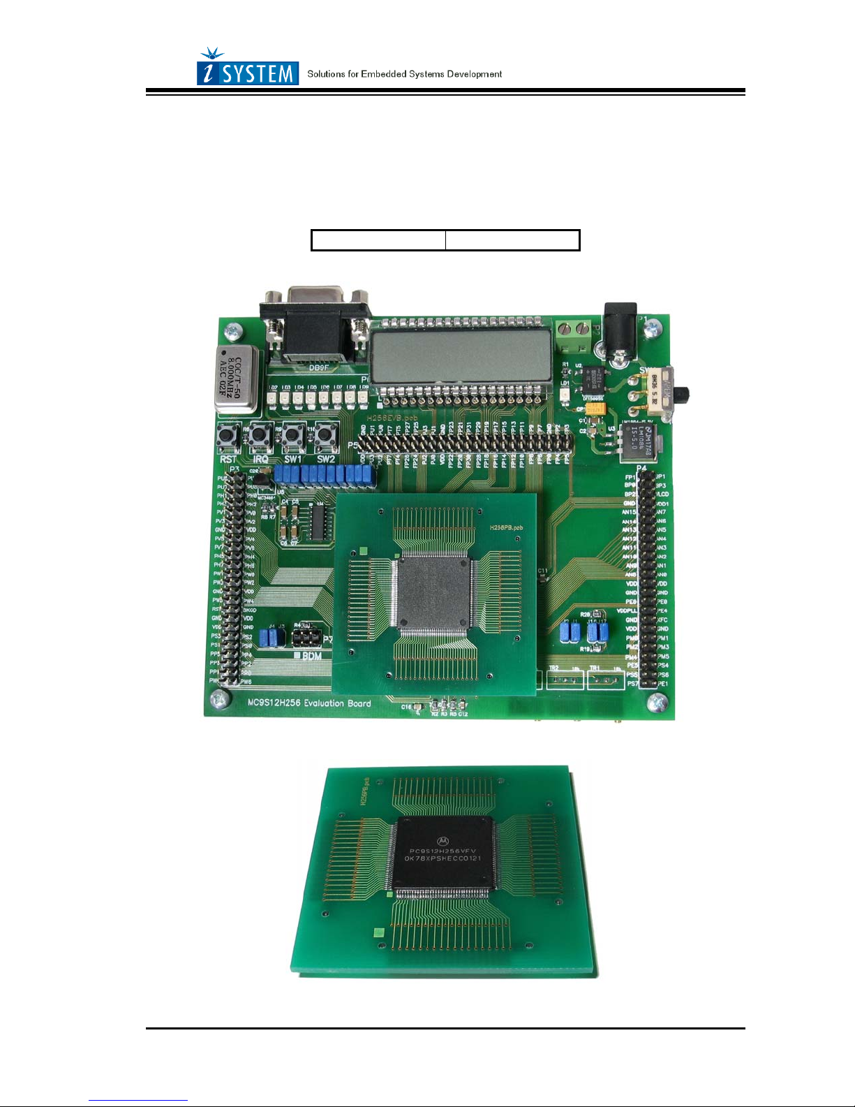
Setting up the board
The MC9S12H256 Evaluation board has been tested and programmed with the demo application.
Please examine the board and check that:
• The LCD module and the crystal oscillator are installed.
• All jumpers (J1-J17) are set.
Standalone operation
• Make sure that the CPU piggyback is installed.
• Plug the DC source (e.g. AC wall adapter) to the P1 connector or apply DC source to the
connector P2.
• Turn on the power switch SW1 and check the green power LED LD1.
• The board should execute a sample application.
Use with MC9S12H256 ActivePOD
• Remove the CPU piggyback from the board.
• Connect the MC9S12H256 ActivePOD to the board.
• Turn the emulator on and then power the target.
• Run winIDEA, open a sample project and carry out the debug reset. The system is ready for
debugging.
Use with BDM debugger
• Make sure that the CPU piggyback is installed.
• Connect the 68HC(S)12 iCARD to a standard 6-pin BDM debug connector P7
• Turn the emulator on and then power the target.
• Run winIDEA, open a sample project and carry out the debug reset. The system is ready for
debugging.
Running winIDEA
It’s assumed that winIDEA is installed on a PC, where iSYTEM development tool is connected.
Contact your local iSYSTEM sales representative for a sample project or download it from:
ftp://www.asystelectronic.si/winidea/samples/targets/itmc9s12h256.zip
Start winIDEA application from the Start menu and open a sample project workspace. If you are using
ActivePOD, open sampleICE.jrf workspace and if you are using BDM debugger, open sampleBDM.jrf
workspace. Next, check if proper emulator hardware is selected and the communication between the
PC and the emulator.
Carry out the debug reset and run the application (debug run) in case of BDM debugger and carry out
the debug download and run the application (debug run) in case of MC9S12H256 ActivePOD.
Blinking red LEDs (LD2-LD9) and a “Welcome” title on the LCD display indicate a working system.
Additionally, a test string is sent to the host RS232 terminal.
There are four push buttons on the board designated SW1, SW2, RST and IRQ. RST resets the
complete system. Make sure that ‘Reset from target’ option is checked in winIDEA when using RST
button and the development system is connected to the board. IRQ turns on all LEDs. SW1 turns on
one LED and shift its position to the left for each consecutive push. SW2 does the same except that it
shifts in the opposite direction.
Trimmer TR1 controls the LCD brightness. Use a mini-screwdriver to adjust it.
Trimmers TR2 and TR3 are connected to the CPU A/D converter. TR2 is connected to the channel 0
and TR3 to the channel 1. Refer to the board schematic for more details.

iSYSTEM, October 2003 4/8
ITMC9S12H256 Operation
Power Supply
The external power supply must provide the voltage between 6 and 12 V DC (typical 9 V DC).
Maximum current consumption shouldn’t exceed 100 mA when 9 V DC is used. The polarity is not
important. Low voltage DC plug must conform to the DIN 45323 standards:
• The hole diameter is 1.95 – 2.5 mm (standard: 2.1 mm)
• The external diameter is 6.2 - 5.5 mm (standard: 5.5 mm)
Note: The emulator must be powered on first, then the target board and vice versa when switching off
the system. First, switch off the target and then the emulator.
Jumpers
All CPU peripheral signals used on the board can be disconnected from the CPU via jumpers. By
removing the jumper, the belonging signal is freed for the user. Note that all CPU signals are available
on the expansion connectors and can be used by the user.
Jumper DESCRIPTION
J1 Enable AN0 (Analog input 0)
J2 Enable AN1 (Analog input 1)
J3 Enable PS1 (Transmit data)
J4 Enable PS0 (Receive data)
J5 Enable PE1 (IRQ push-button)
J6 Enable PH0 (LD2)
J7 Enable PH1 (LD3)
J8 Enable PH2 (LD4)
J9 Enable PH3 (LD5)
J10 Enable PH4 (LD6)
J11 Enable PH5 (LD7)
J12 Enable PH6 (LD8)
J13 Enable PH7 (LD9)
J14 Enable PE0 (SW1 push-button)
J15 Enable PM0 (SW2 push-button)
J16 Enable PE6 (MODB=0)
J17 Enable PE5 (MODA=0)

iSYSTEM, October 2003 5/8
LCD display
ITMC9S12H256 evaluation board uses 8-character LCD glass display. Each character consists of 14
segments. Following figures shows the segment position and a decoding table.
PIN COM1 COM2 COM3 COM4 PIN COM1 COM2 COM3 COM4
1 1D 1E 1F 1S 19 NC NC COM3 NC
2 1J 1I 1H 1G 20 NC NC NC COM4
3 2D 2E 2F 2S 21 8DP 8C 8B 8A
4 2J 2I 2H 2G 22 8K 8L 8M 8N
5 3D 3E 3F 3S 23 7DP 7C 7B 7A
6 3J 3I 3H 3G 24 7K 7L 7M 7N
7 4D 4E 4F 4S 25 6DP 6C 6B 6A
8 4J 4I 4H 4G 26 6K 6L 6M 6N
9 5D 5E 5F 5S 27 5DP 5C 5B 5A
10 5J 5I 5H 5G 28 5K 5L 5M 5N
11 6D 6E 6F 6S 29 4DP 4C 4B 4A
12 6J 6I 6H 6G 30 4K 4L 4M 4N
13 7D 7E 7F 7S 31 3DP 3C 3B 3A
14 7J 7I 7H 7G 32 3K 3L 3M 3N
15 8D 8E 8F 8S 33 2DP 2C 2B 2A
16 8J 8I 8H 8G 34 2K 2L 2M 2N
17 COM1 NC NC NC 35 1DP 1C 1B 1A
18 NC COM2 NC NC 36 1K 1L 1M 1N
Decoding Table

iSYSTEM, October 2003 6/8
Connectors
RS232 connector BDM debug connector
Pin DESCRIPTION
P1 N.C.
P2 TxD (Transmit data)
P3 RxD (Receive data)
P4 N.C.
P5 GND
P6 N.C.
P7 N.C.
P8 N.C.
P9 N.C.
Expansion connectors
All CPU signals are present on the expansion connectors (P3, P4 and P5).
PU5 1 2 PU4 FP1 1 2 BP1 VDD 1 2 GND
PU7 3 4 PU6 BP0 3 4 BP3 PU3 3 4 PU1
PH1 5 6 PH0 BP2 5 6 VLCD PU2
5 6 PU0
PH3 7 8 PH2 GND 7 8 VDD1 PT7
7 8 PT7
PV1 9 10
PV0 AN15 9 10 AN7 PT4
9 10
PT5
PV3 11 12 PV2 AN14 11 12 AN6 FP26 11 12 FP27
GND 13 14 VDD AN13 13 14 AN5 FP24
13 14 FP25
PV5 15 16 PV4 AN12 15 16 AN4 PJ2
15 16 PJ3
PV7 17 18 PV6 AN11 17 18 AN3 PJ0
17 18 PJ1
PH5 19 20 PH4 AN10 19 20 AN2 VDD 19 20 GND
PH7 21 22 PH6 AN9 21 22 AN1 FP22 21 22 FP23
PW1 23 24 PW0 AN8 23 24 AN0 FP20
23 24 FP21
PW3 25 26 PW2 VDD 25 26 VDD FP30
25 26 FP31
GND 27 28 VDD GND 27 28 GND FP28
27 28 FP29
PW5 29 30 PW4 PE6 29 30 PE0 FP18 29 30 FP19
~RST 31 32 BKGD VDDPLL 31 32 PE4 FP16 31 32 FP17
GND 33 34 VDD GND 33 34 XFC FP14
33 34 FP15
VDD 35 36 GND VDD 35 36 GND FP12
35 36 FP13
PS3 37 38 PS2 PM0 37 38 PM1 FP10 37 38 FP11
PS1 39 40 PS0 PM2 39 40 PM3 FP8 39 40 FP9
PP5 41 42 PP4 PM4 41 42 PM5 FP6
41 42 FP7
PP3 43 44 PP2 PE5 43 44 PS4 FP0
43 44 GND
PP1 45 46 PP0 PS5 45 46 PS6 FP4
45 46 FP2
PW4 47 48 PW6 PS7 47 48 PE1 FP5 47 48 FP3
P3 P4 P5
BKGD 1 2 GND
N.C. 3 4 ~RST
N.C. 5 6 VDD

iSYSTEM, October 2003 7/8
Schematic

iSYSTEM, October 2003 8/8
This page left blank intentionally.
This manual suits for next models
1
Table of contents