Jade ISO-BUS User manual

JADE COMPUTER PRODUCTS
Presents
THE
ISO-BUS
MOTHERBOARD
JADE COMPUTER PRODUCTS
TECHNICAL SUPPORT GROUP
l4901 WEST ROSECRANS
HAWTHORNE", CA 90250

I
iTHE ISO BUS
J:
a
e
:One oí the most important--and most often overlooked --pieces of equipment in any '
jcomputer system is the motherboard. Far from being just apassive hunk of epoxy or i
jfiberglass with abunch of copper traces running around hither and yon, it is an active and g
iintegral part of the system--the very íbundation of your computer. :
g
:You have just made the very wise decision to purchase one of the best motherboards in t
:existence: the JADE ISO—BUS '" Motherboard. Now that's apretty sweeping statement, so
iwe'd like to tell you why we feel that we can make it 1r good conscience. Along the way, S:
'hopefully, you'll get afew laughs while you're learning.
g
:¿
Y
d
'ASHORT HISTORY OF SOME BAD MOTHERS
A
!OK, let's face it. Not ali mothers are good. And just as in the real world there are good
:mothers and bad mothers ,so there are good motherboards and bad motherboards, and
;some of the bad ones are real bad mothers. Of course, if your mother is bad, you keep very
:quiet about it.
·á
:In the early days of hobbyist computers, amotherboard was considered to be just
Z
'something that had alot oí" convenient etched wires running around the place to which
y
iconnectors could be attached to hold the little darlings--all the various computer cards.
Then the "little darlings" began to grow up, and started running around at 2and 3and 4
MegaPiertz instead of lolling about at 125 or 250 or 500 KiloHertz, and people began to
discover strange eccentricities in their signals. It began to dawn upon them that a
motherboard was supposed to be something more than just abunch of wires, because what
ycu had at those frequencies was 95 or so little antennae, all interacting, putting out gobs of '
RF radiation (neatly screwing up Channels 2-S of all the local TV receivers).
it seemeg the mothers were gossiping over the back tence, aíid those nice theoretical square
waves that their children were supposed to be speaking turned out to be not so square. In fact,
these iii-mannered children had real garbage mouths. Their speech looked like somebody's
iunmown i'ront yard with oodles of liítle grassy spikes all over the place. (See Oscilloscope
iPhím i). in fact, there was as much confusion, with listeners trying to be talkers and talkers
irambling Oíl and on, as there is at apoiiticai convention. The wonder was that anything got
iGÜí.é- ;j¿ .jcQ)ié began to learn that good mothers don't lean over the back fence gossipping
!while :íever íeiiing their children to shut up.
S
,) Z"Áé first stage cure íoi" this problem was to ground one side of the motherboard with anice
;1 wA- ground glaíie. The problem with this approach is that anytime you run aground plane
,or- -.'Áé other Líe Üi asignal line, with afiberglass or epoxy board in between, what you get is a
:3a">uciíor. (:'¿jt':í"iass, el ai, makes an excellent dielectric, you see).
'Z
j3j iiú'w y\c.¿¿¿ you had was tuned RF antennae.
IFKt."'iaL'.á'¿e: yíbr the world, mothers have atendency to improve ?y"Új experieme. And so do i
?:..,7,.Á¿'¡"b.:j[u3 .ziui the engiáeers wP.o design them. i
iii
i

The next thing we noticed about mothers was that some of them let their children run hog
wild. This phenomena is called "ringing" (See Oscilloscope Photo 2). Accordingto Murphy's '
Law, no sooner do you think you finally have your kids straightened out than something else
comes along to gum up the works. To corral the little buggers and make them walk the
straight and narrow, anew feature was added to motherboards, called terminators.
There are two types of terminators: active and passive. Apassive terminator is nothing
more than two resistors, one going to avoltage supply and the other going to aground, with
the signal line tied between, and sometimes abypass capacitor which is supposed to short the
high-frequency stuff no one is interested in to ground.
There is aproblem with this approach. All those resistors gobble up power, and they've no
place to dine but the signal; q.e.d. the signal's power gets eaten. Also, there is aspecific time-
constant involved anytime you connect acapacitor to aresistor, and unless you do it exactly
right (which most board designers don't), you foul up the rise and fall times of the signals.
Active terminators are a little bit better. They're about the same as a passive terminator,
the exception being that in aproperly designed active terminator the power drain doesn't
come from the signals that are being terminated, but from the central power supply through
an active component like an op amp.
This cured the ringing--somewhat. But engineers are sometimes like economic
theoreticians--they attack the symptoms and neglect the root causes. And despite all these
approaches, the basic problem of the bad mothers was still there: 95 or so little antennae, and
lots of crosstalk.
Enter JADE.
JADE engineers--being halfway intelligent (or maybe just lucky), and of that peculiar
breed that aren't snowblind--finally hit upon the solution; the JADE ISO—BUS '". The
theory being: if you've got something noisy, put it in anice quiet box--if you surround awire
with ashield that is grounded, it can't radiate.
The ISO—BUS '" is the result and the practical application of that theory--and it works as
slick as a greased pig at acounty fair.
Net only is each and every signal line surrounded on both sides by aground line (thereby
preventing crosstalk), these ground lines are interwoven, top and bottom, into amesh. This
isn't the place to go into network mesh theory, but if you're interested there are several good
books on the subject although they're alittle bit on the esoteric side.
In areal-world sense, the signals think they're running between two infinite ground planes,
sq they stay very quiet and well behaved. But at the same time, the ground planes know
they're amesh network, so they have aminimal capacitance effect.
Asecondary benefit--and this might be one of the most important side effects--is the
inductive reflectance. As asignal reverses in aline, it carries along with it amagnetic field.
This magnetic field sweeping along the line induces acurrent flow in the next signalline. But
the next signal line--on either side and top and bottom--on the ISO-BUS"" is aground line.
This line mirrors the inductive effects of the signal line, and eliminates it.
What all of this technical-sounding gibberish boils down to is that the JADE ISO—BUS '"
is agood mother board. It takes tender care of its children, holding them gently in its claws,
2


and it sees to it that they are quiet and well-behaved--speaking only when they're supposed to
and shutting up otherwise.
It is SO good, in fact, that it will NEVER need termination, either active or passive. The
distributed capacitance-inductance of the network mesh acts to prevent ringing . . ..as an
added bonus, because the layout was done precisely enough to provide just the exact
capacitance to prevent it. The 95 or so noisy antennae magically disappear and you have
,exactly what you're supposed to have: signal lines running quietly to various cards. (For
,proof, check out Oscilloscope Photo 3).
'SOME SPECIFIC WARNINGS:
There are some problems connected with the ISO—BUS'" Motherboard. Because they are
iso precisely laid out, the leads run very close together. Although JADE has taken the trouble
,to use the most modern solder-masking techniques, it is possible to create solder bridges. So
)if you're heavy-handed with the soldering iron, beware. Too much heat, and the application
A
:of too much solder, will almost inevitably result in aphenomenon called "wicking", which
jmeans that the solder runs down the pins of the connectors and puddles up on the component
}side of the board, very neatly shorting out the signal lines to the ground lines.
jYou should be aware that JADE will not guarantee nor repair any board that is purchased
Y
ias a kit. All ISO—BUS '" Motherboards are tested individually for continuity and inter-line
Ishorts before they leave our manufacturing facility, so we know they're good when they leave
Ihere. Unless you're areal artist with the soldering iron, don't even attempt to put this board
together by yourself.
If you do insist on buying it as akit, please be aware that JADE'S policy is as stated above.
(Since solder bridges are most likely to occur underneath the connectors on the component
Iside of the board, the board is useless because the connectors are too difficult to unsolder
'without destroying the board in the process. It has to be scrapped, and we will not guarantee
:it. For those hard-core people who buy the board as abare board, please make certain to use
the proper connectors. We strongly suggest that you buy them from JADE, because we've
already gone through the hassle of finding the right connectors that are the least susceptible
!to wicking and other nasties.
WARNING: The JADE ISO---BUS'" is manufactured to conform to the proposed IEEE
S-íOO bus standards. This specification provides for ground lines on pins 53, 20, and 70 in
Iaddition to the old ground tines at pins 50 and !00. There are a few boards which use these
!pins for signals.
:Under the old definitions, pin 53 was Sense Switch Disable*. Many CPU boards
i(iñciuding the JADE IA,/Z80 and BIG Z) use this line. Under the IEEE definitions it is a
Iground line. This cffectiveiy halts the CPU, therefore the pin on the CPU card must be cut. If
)the signal is required for afront panel, it may be routed over the jumper cable connecting the
jCPU with the front banei board.
IPins 20 and 70 were formerly defined as Memory Protect) Unprotect respectively. Under
iíhe IEEE definitions, úíese are both grounds. This may create some problems with older-
3

i" '"style memory boards which use this feature. You should update your boards to conform to ,
ithe IEEE S-iOO Bus Standard Pinout enclosed in this manual. For most boards, this is a
relatively simple íix, and many boards will not even have to be modified since the S-tOO
standard was designed to conform to the configuration of as many S-lOO-style cards as t
possible.
.ifyou have aproblem with aboard and do not know what to do about it, send aXerox or
,oíher copy of your board's schematic or circuit diagram to JADE COMPUTER
PRODUCTS, TECHNICAL SUPPORT/ENGINEERING, 4901 W. ROSECRANS,
HAWTHORNE, CA. 90250, with astamped, self-addressed envelope, and JADE will do a
paper study for you without cost. Incidently, this service is available for compatiblity
problems on all the boards we sell.
MAKING IT——FOR THE REAL HARD-CORE
CONSTRUCTION AND SOLDERING TIPS
wChoose avveil-iighted work space with enough room to place yourtools, parts
and instructions. If you have two light sources that can be adjusted, this wili help
eliminate shadows which interfere with seeing your work.
2
3Familiarize yourself with ali of the general operations to be performed. It t'
Imight even help to do adry run. )
?
&The toots you will need for each individual kit will be listed in the assembly .
instructions. Abasic set would include: alow wattage soldering iron (20 watts or less), )
and with a650" tip ifyou can get one, aholder which will keep you from accidentally l
í'ouchmg the hot up, apair of wire cutters (also called dykes or skle cutters, preferably j:
beveled so that you cari cui close to the board), apair of needle-nose pliers, adamp :'
lsponge or amoistened cloth to use to wipe ihe soldering iron's tip, amagnifying glass (
ito Fxamine details, and alead former to bend leads. The latter is available at most t
;e1ecíron,tcs parís houses in an inexpensive plastic version, or you can make your own
out oí 'wood, Ifyour're kíto building lots of electronic kits, they're worth their weight I
in goid. )
)6Arrange your tools iii order oí their frequency oí use and orient them so
ithey're easy to reach. Make sure that they are clean and in good working order. t
:
t
wKeep your work area clean and uíicluttered.
'i'
L
@Make sure that your chair is set at aproper height and is comíortabk for your ;-:
work station.
Z
4

b
bTry to keep food and drink away from your area. Always strive for neatness
and uniformity. This means removing bits and pieces ofscrap wire and solder blobs, as
you work so they don't become buried in your board and short something out.
lneveitably, according to Murphy's Law, they will sneak underneath IC sockets, and if
there is aplace that's hardest to get to to fix, that's exactly where they'll lodge.
bSoldering can cause several different kinds of problems in kit building. Heat
can damage the PC board and the components, especially diodes and transistors, or
create unwanted electrical connections. Most problems can be eliminated by using ,
the right soldering iron (and the right solder--resin core, NOT acid core), and by
developing an efficient technique.
wParts are inserted on the component (front) side of the board. Soldering is
done on the back side. This is always arule, unless you are specifically directed
otherwise in the assembly instructions.
wIf you plan on building many kits (and one memory board can be many kits),
spend the few extra dollars to buy yourself aquality temperature-controlled soldering
station. Spending the $30 can save you from ruining a$200 kit.
wUse only ROSIN CORE SOLDER when constructing electronic kits. Never,
never, not ever use acid core--that's only for pipes and sheet metal. Asolder with ahigh
ratio of tin to lead is important. 60/40 is good, but 63/ 37 is excellent, and the
difference will amaze you. If you can't get 63/ 37 at your local electronics parts house,
JADE carries it.
nMake sure you have awell-tinned tip. Atip is well tinned when it has athin
film of solder coating on the surface of the iron. Oxide and resin will build up as you
work with it and the bright shiny look will disappear. That's what the wet sponge or
moistened cloth is for. The iron should be wiped clean about every ten connections or
so to get rid of that oxide and resin. Copper-tipped irons are fairly good, but gold-
coated ones are much better.
wSome DON'Ts: DON'T have any unnecessary items at your work station.
DON'T use worn or damaged tools. NEVER solder equipment that is plugged in.
DON'T use unknown cleaning solutions. DON'T pull on asolder joint to see if it's
good. NEVER flip excess solder from the tip of your iron--use the sponge or cloth.
NEVER put solder on your iron and then transfer it to acold joint.
mHeat both the component wire and the solder pad with the tip ofthe iron until
it looks wet or liquid. Then touch the solder to the junction between the iron, the pad
and the wire. When the solder melts and flows onto the connection, quickly remove the
5

J
iron's tip. Allow the joint to cool without moving any ofthe components. Agood joint
¡will be smooth and bright. Abad one will be adull lead-looking glob of solder.
·AVOID USING TOO MUCH SOLDER. From our experience at repairing
customers' boards, this is the sin most often committed. Iflittle drops ofsolder appear
on the opposite side of the board, you're either using too much solder or too much
heat. Be extremely careful when you solder adjacent pads because the heat may cause
4the solder to flow between them, making asolder "bridge". Bridges are only good for '
!crossing rivers--they don't belong on electronic boards. They make an unwanted
electrical connection.
eIf you do find abridge, the best way to remove it is to clean your iron on the ,
dampened sponge and then touch the bridge with the clean hot tip until it wets and
sticks to the tip. Then get rid of it.
i
wExcess wire can be removed with diagonal cutters. WAIT till the joint has
cooled. Beware of flying pieces of wire. ALWAYS USE EYE PROTECTION
,WHEN SOLDERING OR CUTTING WIRE.
wAfter you're ali done, use Freon solvent to remove the flux. Flux is that "
brown stufí that gets on the boards near your soldering joints, and it is formed of
burned rosin. Not only does it look bad (preventing your wonderful soldering job from
!looking ali bright and shiny), it can cause electrical headaches as well, especially in
higher-frequency circuits. Not only this, but it makes it much more difficult to find
bridges and shorting flakes, since the resin hides the solder under an effective coverup.
Leave coverups to politicians--clean your board.
)aJADE technical support people have found that aboard works about like it
llooks. Ifit's been put together with care and good workmanship, it will workjust fine.
)in life, you only get out of it what you put into it, and it works the same with electronic
kits.
2ASSEM3LY INSTUCTÍONS FOR THE JADE ISO-BUS'" S-lOO IEEE i
STANDARD MOTHER BOARD
j
Vile suggest you start at atime with you will be able to complete it without '
)interruption. Mark the check ()as you do each step. This kit could be assembled in
several ways, but if you follow these step-by-step directions your assembly problems .
should be fewer. ,
t( ) l. Make sure you've the tools needed. For this kit you need the following: asoldering'
iron (20Watts Maximum), ROSIN COR Esolder (preferably 63/ 37), cutters,a small'
magnifying glass, ascrewdriver, and alead former.
6

()2.Check the PARTS RECEIVED against the PARTS LIST. Take special care to)
correctly identify look-alike parts; i.e., resistors, capacitors and diodes. If anything is
missing, please yíli JADE's Customer Service Department.
()3.Read the section called: Construction and Soldering Tips.
PCAUTION: USE EYE PROTECTION WHILE SOLDERING OR CUTTING
WIRE! i
()4.Begin the assembly by inserting the lOO-pin edge connectors into the Motherboard.
You will notice that there are rows of plated-though holes between the holes for the
connectors. These have been arranged so that it is impossible to insert aconnector into
them. It is not necessary to inspect the board for plating errors, since this has already
been done during manufacturing. Every board is thoroughly checked for continuity
and shorts between leads.
()5.The S-lOO connectors should all face the same way. Place the side with the writing
toward the front of the board. The front of the board is the edge that has the JADE
insignia on it, and the top of the board is the side that is marked "connector side".
()6.When all the connectors have been inserted, place the foam lid of the shipping-
container firmly against the top of the connectors and carefully turn the board over,
pressing it firmly down onto the table top.
:()7. inspect the connector pins to make sure that all of them came through in their
proper holes, and none of them have gotten bent under.
j()8. Solder pins Iand lOó of each connector, on adiagonal line across the connector.
()9.Now turn the board over and carefully inspect the placement of this connectors.
They should be flush with the top of th board. This is IMPORTANT, since the proper,
placement of the connectors will help prevent wicking. Ifany of them are floating off
the top of the board, carefully heat the corner pins whiie.pushing down on the top ofj
the connector.
!()iO. Turn the board back over and solder all the connector pins. It is helpful to do one
:entire row oí pins at atime. Don't leave the job with apartially-soldered row, since it is
ieasy to overlook unsoldered pins. If you have to leave the job, wait until you've
ifinished awhole row.
S
!
1( )li. When you're ready to solder ajoint, apply heat to the joint first, then apply the
!solder to the oppcsite side of the joint from the iron. (See figure i). Then remove the
i' 7

)solder, and firiaiiy remove the soldering iron. JADE has reflow-soidered these boads,)
gív'hich meaíís that they already have some solder on them, so don't use too rnucM
t
)solder. As soon as the joint looks wet and begins to liquify, apply the soldé: ". Thij
isjíQü!ci tate abüut two seconds with adecent iron. The iron should not be left on the
)joint longer than two or three seconds after the solder has been first applied. Agot: íi
,iúkki" joint has an even flow of solder over the entire joint. abad soider joint,'
Icommorüv called a"cold" solder joint, will have adull, lead-like appearance. Do tiíjt
move ílie part or the board while the solder is cooling, or acold or fractured solderi
joiríí will result {See figure 2). I
l
1( )í2. Patience is avirtue, especially when assembling Motherboards. On asix sloíj
íSO---BU S'" there are over 600 connections to make 1200 on the twelve slot, and J900 '
ion an eighteen slot. Every one of these must be perfect. The board was designed to be
,wave-íkm' soldered. ifyou do not have the patience to correctly assemble it, return the
)baz"c bcard or the kit NOW and buy an assembled unit. JADE will NOT guarantee,
Irepair or replace any ISO-BUS'" Motherboard assembled from abare board or kit. '
j
\'
)()í3.'Niíen the connectors have been soldered in place, take an ohmmeter and place the
)cymmon lead on aground. Test each and every signal point on every connector for a
jsñoet ío µrouñd. Then íest adjacent signal traces. (Pin Iagainst 51 and pin 2: pin 2
:against pin i, 51, 52, 53, and 3, etc.). if wicking has occurred and aglob of solder is
)shórtiiíg olú the traces the short is most likely to occur between asignal line and
3,
;gi"ouríd, anti is Mscj most likely to be located underneath úie connectors on the top of I
íhe bc'ard. (See "WHAT TO DO IF MURPHY'S LAW GETS PASSED" for how to
fix Li. And our sympathy is with you.) :
)( )14. If the Zioáííl has come this far, congratulations, You're areal artist with the i
isokk:"irig iron. Now comes the easy part. <
1( ):S Fbi-m the resistor as per Figure 3, and insert it at the rear right of the board (See I
!Compóríent Placement Diagram). Solder it and cut off the excess leads. )
'( )16. F'txiñ the LED diode leads as per figure 4, and insert it. Solder it and cut off the
)
j'XCt'SS leads. Dg NOT insert it backwards. Make certain that the cathode side goes Í
zouarc! the bar orí the diagram on the board. (See Component Placement Diagramj· !
i{
( ) i7. Sit back, relax, survey your workmanship and treat yourself to anice long drink- )
you deserve it! !
i
é
.
é
ft
}
i
i
jI
4,.8

COMPONENT INSTALLATION
Install all components in their proper location, and ifpolarity is important, observe
the proper markings. The component should be installed flush with the circuit board,
unless aclearance is specifically called out. This clearance is usually required for hot
components that might burn or discolor the printed circuit board.
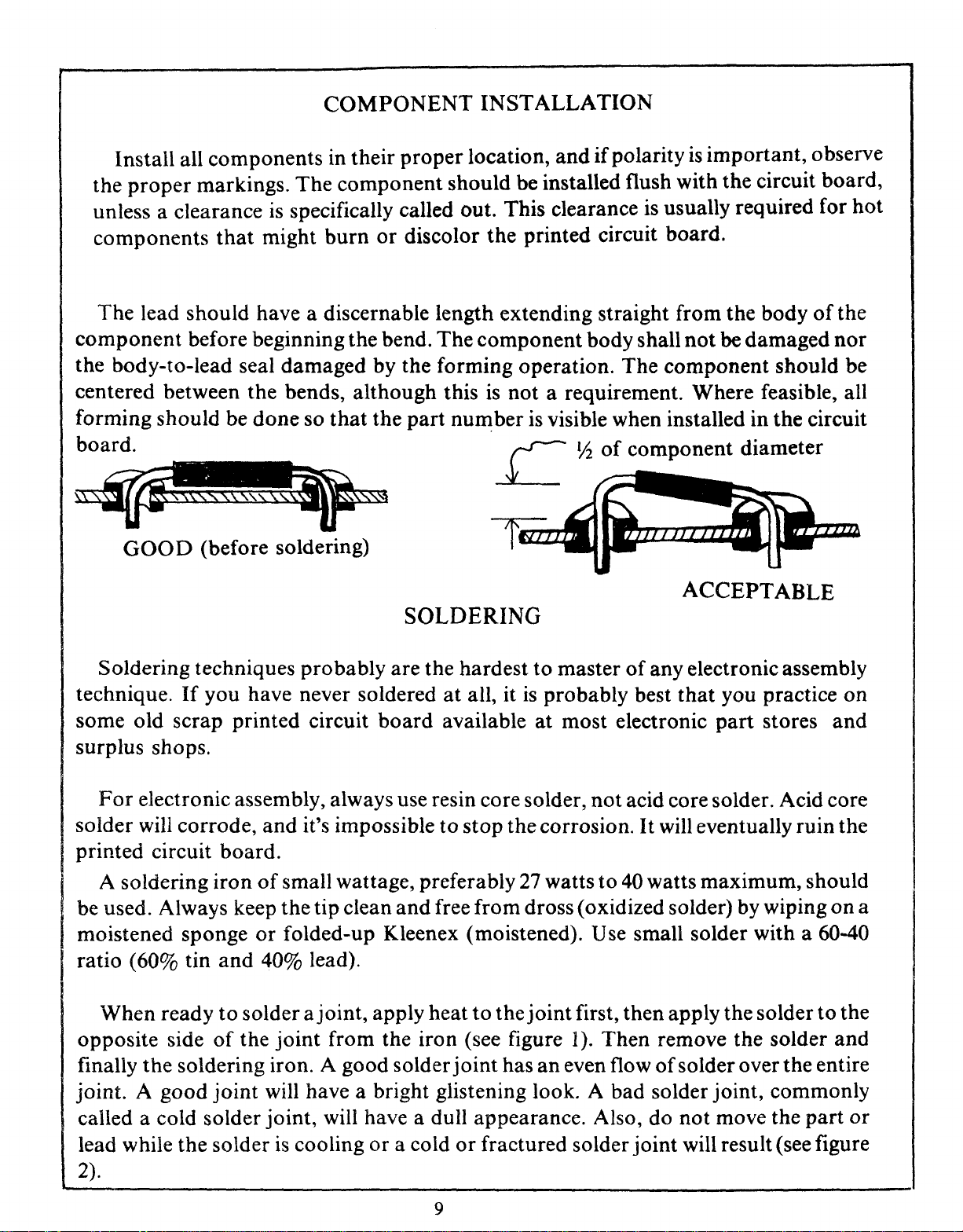
The lead should have adiscernable length extending straight from the body of the
component before beginning the bend. The component body shall not be damaged nor
the body-to-lead seal damaged by the forming operation. The component should be
centered between the bends, although this is not arequirement. 'Where feasible, all
forming should be done so that the part number is visible when installed in the circuit
r"'A of component diameter
GOOD (before soldering) 'A^b=
ACCEPTABLE
SOLDERING
Soldering techniques probably are the hardest to master of any electronic assembly
technique. If you have never soldered at all, it is probably best that you practice on
some old scrap printed circuit board available at most electronic part stores and
surplus shops.
For electronic assembly, always use resin core solder, not acid core solder. Acid core
solder will corrode, and it's impossible to stop the corrosion. It will eventually ruin the
printed circuit board.
Asoldering iron of small wattage, preferably 27 watts to 40 watts maximum, should
be used. Always keep the tip clean and free from dross (oxidized solder) by wiping on a
moistened sponge or folded-up Kleenex (moistened). Use small solder with a60-40
ratio (60% tin and 40% lead).
When ready to solder ajoint, apply heat to the joint first, then apply the solder to the
opposite side of the joint from the iron (see figure I). Then remove the solder and
finally the soldering iron. Agood solder joint has an even flow ofsolder over the entire
joint. agood joint will have abright glistening look. A bad solder joint, commonly
called acold solder joint, will have adull appearance. Also, do not move the part or
lead while the solder is cooling or acold or fractured solder joint will result (see figure
2).
9

i\ |i
1| IiSOLDERING technique
lIIPAD
i
SOLDER
"1
figure lLEAD
—)
APPLY SOLDER TO OPPOSITE SIDE OF LEAD
FROM THE SOLDERING IRON. SOLDERING IRON
FIGURE 2a OPTIMUM JOINT
THE FILLET IS WELL ...-..:·:.·.·:.[,":·:.'.i.:·.-....
FORMED. CONCAVE .
..·,:::::::)':ij.'i'i:::!::'::::::::.::::::;j:::·:.i::::?::·:::':::.
AND WELL ABOVE THE i,.CLIMBED UP LEAD .'.·': ":"·'"·""·'"·""""·'"·""""·'.:'·""·;·:.:...·:.:......
SURFACE OF THE PAD .. .i.. .'.: .'..".:".'"."'"'"' "' "' '"""""".".'..
··:;j¿' :"""' -··-.··: -·:·.·:·..:¿·;·::·:=;·";':·;;:':·;':'%·:::.·::..
·" .··...· .¿i: :"' "' '''·"·"·'·"'·.'·..'.: ·.'.·.'::·,m.':""'"·¶,:. ".·:·'·":':·:':':':i:ii'i·::':·::':·
' ".. ' '" ' ·,. ·:;".;·.'.·.,·. ·... ·.'
::· ·..:·.:·.'.·..'-".·.'·.'·.
.. ......... ..... .......
· ,·. ·. "' ·:·.'·: '' "
.. ... .. .. .............
bo^r"Y///R :,,
::j>Ui:,,:"
:,';',",":1 >:""""";"";'j";'j""
.,.:'.'::. ··': ... I, ....... .. . .
'CIRCUIT ""'¿¿'t'. ,-,',',','.'""""" "'.::.::.::.:..:,.:..:..:..:..:.:::.::. '" "" '··'··:"·;'";'"""'
SOLDER W7'·"' FEATHERED EDGES "'": :::::::: ;: ;:; :::':::'..::: :'; ::::':"i,':.:!::,::.:..::..':,:"'
.......... ..... .. ..
.."-.".'".".':':,·;Z"-
LEAD '"·'.':·:·::::::::::::·:';::::::::::::':-::':·:.':·:.:.':·"' TOP VIEW
SIDE VIEW '" '""
THE SOLDER MUST BE CLEAN, SMOOTH AND BRIGHT
MINIMUM SOLDER ACCEPTABLE
SOLDER FIGURE 2b
Á///k)'" )'"íU j:")' "" '").'").: ,:,,
\' 'I)"
... .,...... .
)SOLDER FLOW RESULTING IN AMiNUTE FILLET RADIUS ON EITHER OR BOTH SIDES
!OF THE BOARD IS ACCEPTABLE
:
INSUFFICIENT SOLDER FIGURE 2C
r-<3 SOLDER .
!Y///a 11//¿ ,' )
j
INsUFFiciENT SOLDER. INDICATED BY LACK OF FILLET '
ON ONE OR BOTH SIDES OF THE BOARD I
l0

figure 2d
j,r component .:\,
=mIe j"m _
/' L'""
.
..
.-.
·y -· '.~
acceptable
stress relief and solder build-up on axial lead components
at least one end of axial lead components shall have adequate
stress relief and absence of solder build up.
less than 25%
2 t l2l2
ilack of adhesion
))) )figure 2e rg
''':'.
... ...
<-.,í; ::::::::. '"i ""·'
...-
... .
:- '. ... ,
not acceptable
lack of adhesion indicated by acceptable
evidence 1the lead is not wet lack of adhesion confined to less
on component side, or 2than 25% of the lead perimeter
the pad is notwetatthe solder shall be acceptable provided the
pad interface. lack does not extend beneath board
surface. if defect extends below
the limit is 10¶, of lead perimeter.
Lead forming
Lead forming is performed by grasping the body of the part with the
.fingers of one hand. With the other hand holding long-nose pliers, grasp the lead near
the body with the taper ofthe pliers defining the length oflead from body ofthe part to
the lead. Bend the lead with the opposite hand to form the bend as in the following
figure. figure 3
bend with
7gfingers of
opposite hand
hand forming operation
©T_ V
,,C", ,U)
r_ _7
P~preferred bend configuration alternate bend configurations
E
ii

INSTALLING YOUR MOTHERBOARD
When you have completed your assembly (assuming you purchased your
Motherboard as akit), and you're ready to install it in your mainframe, here are a few
tips and hints that will help you with atrouble-free installation.
l. Connect ALL power leads, using #14 gauge wire minimum. There is areason for
this: On the 6, 12, and 18-slot Motherboards, there is one lead for each voltage supply
"and one iead for ground for each 6slots. These are distributed, from the lead pads, in a
'particular pattern which will help to minimize noise. In particular, you should always
provide as many ground leads as possible.
.2. Use ALL the holes for mounting the Motherboard. This will make it as stiff and
unflexible as possible. Ifyou do not choose to do this, then don't skip more than every
other mounting hole. Above all, don't try to get by with abolt at each corner.
'3. Agood installation would provide aplexiglass sheet underneath the
Motherboard. This both insulates the Motherboard from chassis ground and makes it
extremely stiff and unflexing. Plexigiass can be obtained at most local hardware stores
or building supply companies.
WHAT TO DO IF MURPHY'S LAW GETS PASSED
If you have assembled your Motherboard and discover that you have (horrors) a
short between asigna! line and ground (which is the most likely problem to occur),
don't despair--it can be fixed. Cut the offending ground lead on BOTH sides of the
connector where the short has occurred, and bypass it to the next ground lead. There
are arow oí piated through holes between the connector rows, and you can pick up
your ground lead on one of these.
Be sure to test your signal paths again after you have make this fix to make sure the
fix didn't create another problem. LED
PARTS LIST You should 'Check figure 4"
have received off here flat side jw
[J GOES TOWARD
JADE ISO-BUS'" Motherboard lbar on
Rl, 220 ohm, V! watt resistor ladiode symbol
(RED, RED, BROWN)
Dl, LED l [J
,S-tOO Card Connectors 6, 12, or 18 CI "Dl
DIODE SYMBOL
l!2

JADE would welcome your comments about this board. We are very much
interested in you, our customer, and we want you to provide us with some feedback
about how you like the product, its manual ,and the completeness and thoroughness
of the documentation provided, so that we can better serve you. JADE would
appreciate your response. Please take amoment and fill out the questionaire and
return it to us at the address below:
JADE COMPUTER PRODUCTS
TECHNICAL SUPPORT GROUP
4901 WEST ROSECRANS
HAWTHORNE, CA 90250 CIRCLE ONE
l. Was your ISO-BUS Motherboard received in areasonable length of time? YES NO
2. Was anything damaged in shipment? YES NO
·3. Were any parts missing? YES NO
If yes, what were they?
4. Was the quality of the material and workmanship good? YES NO
'5. Did you have any trouble understanding the manual? YES NO
If yes, in what area/s?
:
:6. Have yoa encountered any problems with the Motherboard? YES NO
.If yes, what?
!
7. Did you solve the problem? YES NO
If yes, how?
'8. Are you dissatisfied with your Motherboard? YES NO
if yes, in what way?
"9. Do you have any suggestions for design improvements? YES NO
'If yes, what?
410. In your opinion, what are the major advantages and disadvantages of the ISO- YES NO
BUS Motherboard?
!1. Other comments?
:12. What is your name, address and phone number?
13

THE PIN 41 DJ2
PIN 42 Di3
PIN 43 Dl7
JADE 1SO~BUS PIN 44 sMl (Instruction Op Code Fetch Cycle Signal)
PIN 45 sOUT .. (Data Transfer to an Output Device)
PIN 46 sINP . . (Data Transfer from an Input Device)
PIN 47 sMEMR (Memory Read)
PIN 48 sHLTA ... ... ... .... ... (Halt Acknowledge)
PIN OUT PIN 49 CLOCK·(2 MPk(2%) 40/60 duty cycle clock. '
No reference to any other bus signals).
PIN SO GND
PIN 51 +8 Volts DC Supply, no amperage specified
PIN 52 -\6 Volts DC Supply, no amperage specifed
PIN 53 GROUND
PIN 54 SLAVE CLR*(Signal from Bus Master to clear
Bus Slave Device) OPEN COLLECTOR
PIN l +8 Volts DC Supplv. no amperage specified PIN 55 DMAO* .. ..... (DMA Request Line) OPEN
PIN 2 +16 Volts Dc Suppiy, no amperage specifed COLLECTOR
PiX 3XRDY PIN 56 DMAI* .. .... .... ... OPEN COLLECTOR
PIN 4ViO* (Vectored Interrupt Lines) PIN 57 DMA2* OPEN COLLECTOR
PIN 5VI!* PIN 58 SXTRQ* ... (Signal Requesting a!6-bit data
PIN 6VÍ2* transfer)
PIN 7Vl3* PIN 59 Al9*
PIN 8Ví4* PIN 60 SIXTN* (Signal granting a!6-bit data transfer
PIN 9VIS* from aBus Device) OPEN COLLECTOR
PIN iO VI6* PIN 61 A20*
PIN li VI7* .PIN 62 A2I*
PIN 12 NMI* .(Non-maskable Jnterrrupt line) OPEN PIN 63 A22 *
COLL"'CTOR .PIN 64 A23
PiX i3 PWR FAIL* ..... .(DC Power Failure, Non- PIN 65 NTD t"· (Not To Be Defined)
maskable Interrupt) PIN 66 NTD (Not To Be Defined)
PIN 14 DMA3* .. .. ... (DMA Request Line) OPEN PIN 67 PHANTOM*. .. ...... OPEN COLLECTOR
COLLECTOR PIN 68 MWRITE*
PIN IS Al8 PIN 69 RFU ....... .. ....(Reserved for Future Use) ,
PIN i6 Al6 PIN 70 GND
PiN !7 Al7 "PIN 7i NTD
PIN 18 STAT DSB* .. .... .. (Status Disable) OPEN PIN 72 RDY OPEN COLLECTOR '
COLLECTOR PIN 73 INT* .... ... ... .... .. OPEN COLLECTOR
PIN 19 C/'C DSB* .... .. (Command Disable?Control PIN 74 pHOLD OPEN COLLECTOR
Disable) OPEN COLLECTOR PIN 75 pRESET".. .... ...... OPEN COLLECTOR
PJN 20 GND (GROUND) PIN 76 pSYNC
PIN 21 NDEF '(NOt to be defined) PIN 77 pWR*
'PIN 22 ADD DSB* .. ......(Address Disable) OPEN PIN 78 pDBiN
'COLLECTOR PIN 79 AO --
PIN 27 DO DSB* .. .. (Data Output Disable) OPEN PIN 80 Al
iCOLLECTOR PIN 81 A2 '"'
PIN 24 gj(B) (SYSTEM MASTER TIMING CLOCK PIN 82 A6 :
iSIGNAL) .PIN 83 A7
PiN 25 pSTVAL* (Status Valid Strobe) PIN 84 AB !
PIN 26 pHLDA ...(Hold Acknowledge to coordinate PIN 85 Al3
"DMA Xfer) PIN 86 Al4 \
PIN 27 RFU .... ... . . .. .. (Reserved for future Use) PIN 87Aíl "
PIN 28 RFU ..... .. .. .. .. (Reserved for future Use) PIN 88 DO2
PIN 29 AS PIN 89 DO3 i
PIN 30 A4 PIN 90 DO7 !
-PIN 3i A3 PIN 91 Dl4 'i
PIN 32 AtS PIN 92 DIS
PIN 33 Al2 PIN 93 DI6 .,
PIN 34 A9 PIN 94 Dll "'
,PIN 35 DOl PIN 95 DIO
PEN 36 DOD PIN 96 SINTA
PIN 37 AID PIN 97 sWO*
PIN 38 D04 PIN 98 ERROR*
PIN 39 DOS PIN 99 POC*
PIN 40 D06 PIN Ilk) GND
14
Table of contents