JHCTech EPI-I981 User manual

EPI-I981
EPIC,4” Industrial Motherboard
Socket G2,3rd and 2nd Generation Intel
Core i3/i5/i7 Processors
User’s Manual
Version:1.00
This publication, including all photographs, illustrations and software, is protected under international
copyright laws, with all rights reserved. Neither this manual, nor any of the material contained herein,
may be reproduced without written consent of the author.
All rights are reserved by Shenzhen JHC Technology Development Co.,Ltd. The information in this
document is subject to change without notice. Please refer to your vendor for the latest information.

- 2 -
Contents
CONTENTS........................................................................................................................................ 2
1 PACKING LIST............................................................................................................................ 5
2 DISCLAIMER .............................................................................................................................. 5
3 TRADEMARKS ........................................................................................................................... 5
4 SAFETY NOTICES...................................................................................................................... 5
5 INTRODUCTION ......................................................................................................................... 6
5.1 SPECIFICATIONS............................................................................................................... 6
5.2 BOARD DIMENSIONS ........................................................................................................ 8
5.3 JUMPERS AND CONNECTORS LOCATION...................................................................... 9
5.4 JUMPERS SETTING AND CONNECTORS ...................................................................... 11
1. RTC1,SRTC1 ............................................................................................................. 11
2. BAT1,BAT2................................................................................................................. 11
3. PS_ON .......................................................................................................................11
4. DC_IN1....................................................................................................................... 11
5. DC_IN2....................................................................................................................... 12
6. U1(SOCKET G2 BASED)........................................................................................... 12
7. HS1,HS2,HS3,HS4(CPU SCREW HOLES) ............................................................... 12
8. CPU_FAN1,SYS_FAN1.............................................................................................. 12
9. U4............................................................................................................................... 12
10. H5/H6 ....................................................................................................................... 12
11. DDR3........................................................................................................................ 12
12. FP1........................................................................................................................... 13
13. VGA1........................................................................................................................ 13
14. INVT1 ....................................................................................................................... 14
15. LVDS1 ...................................................................................................................... 14
16. DVI-I ......................................................................................................................... 15
17. DP1 .......................................................................................................................... 15
18. JP1 ........................................................................................................................... 15
19. COM1....................................................................................................................... 16
20. COM2,COM5............................................................................................................ 16
21. JP3 ........................................................................................................................... 16

- 3 -
22. COM6....................................................................................................................... 16
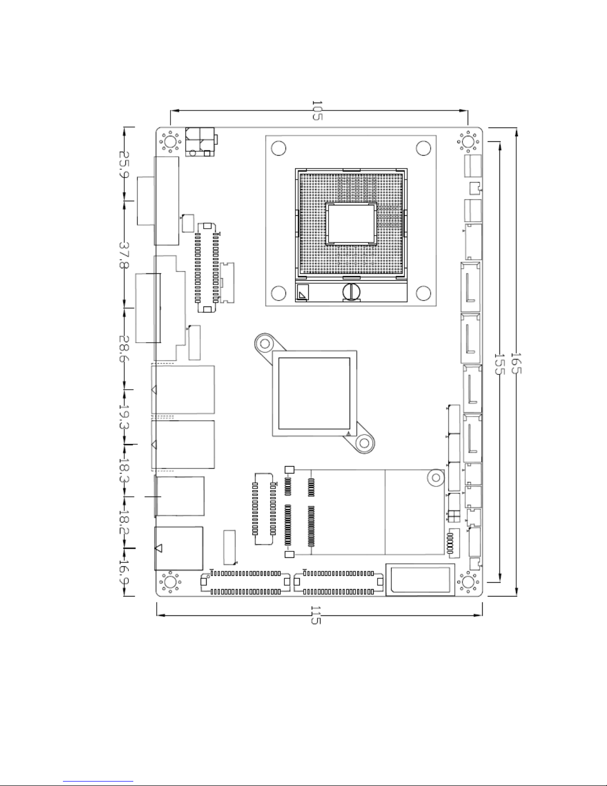
23. LAN1,LAN2 .............................................................................................................. 17
24. USB45...................................................................................................................... 17
25. USB3........................................................................................................................ 17
26. AUDIO ...................................................................................................................... 18
27. SIM1 ......................................................................................................................... 18
28. LED1,LED2,LED4..................................................................................................... 18
29. PCIE_104 ................................................................................................................. 18
30. M-PCIE1................................................................................................................... 18
31. H1............................................................................................................................. 18
32. BUZ1 ........................................................................................................................ 18
33. MIO1......................................................................................................................... 18
COM3(RS422/RS485) ............................................................................................. 18
COM4(RS232) ......................................................................................................... 18
USB3,USB12 ........................................................................................................... 18
PSON....................................................................................................................... 18
34. MIO2......................................................................................................................... 19
GPIO ........................................................................................................................ 19
PS2 MS,PS2 KB ...................................................................................................... 19
USB6,USB7,USB8,USB9......................................................................................... 19
PSON....................................................................................................................... 19
RESET ..................................................................................................................... 19
HDD_LED ................................................................................................................ 19
BUZZER................................................................................................................... 19
35. SATA_P1,SATA_P3 .................................................................................................. 20
36. SATA_P2 .................................................................................................................. 20
37. SATA1,SATA2(SATA3.0)........................................................................................... 21
38. SATA3,SATA4(SATA2.0)........................................................................................... 21
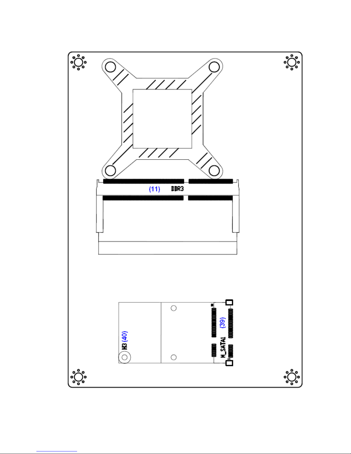
39. M_SATA1.................................................................................................................. 21
40. H3............................................................................................................................. 21
41. ECB-141 (OPTION).................................................................................................. 21

- 4 -
LED2 ........................................................................................................................22
S1 (PWR BT /LED)...................................................................................................22
COM3.......................................................................................................................22
COM4.......................................................................................................................23
USB10,USB11..........................................................................................................23
APSON1...................................................................................................................23
CF ............................................................................................................................ 23
MIO1........................................................................................................................24
45. ECB-142(OPTION)...................................................................................................25
LED2 ........................................................................................................................25
S1 (PWR BT/LED)...................................................................................................25
COM3.......................................................................................................................25
JP4........................................................................................................................... 26
COM4.......................................................................................................................26
USB10......................................................................................................................27
USB11......................................................................................................................27
CF ............................................................................................................................ 27
GPIO........................................................................................................................27
PS_ON.....................................................................................................................28
MIO1........................................................................................................................28
6 BIOS SETUP DESCRIPTION..................................................................................................30
6.1 OPERATIONS AFTER POST SCREEN..........................................................................30
6.2 BIOS SETUP UTILITY.....................................................................................................30
6.3 MAIN SETTINGS............................................................................................................. 31
6.4 ADVANCED SETTINGS..................................................................................................32
6.5 CHIPSET SETTINGS......................................................................................................40
6.6 BOOT SETTINGS...........................................................................................................47
6.7 SECURITY SETTINGS....................................................................................................49
6.8 SAVE & EXIT SETTINGS................................................................................................50

- 5 -
1 Packing List
Thank you for purchasing an JHC Product!
Open the motherboard package and check for the following items. If the motherboard or
accessories are found damaged or missing, please contact your distributor immediately.
●1 xEPI-I981 4” Industrial Motherboard
○3 x Serial Cable (option)
○4 x SATA Cable (option)
○2 x SATA Power Cable (option)
○1 x Audio Cable (option)
○1 x Driver Utility CD (option)
○1 x ECB-141 I/O Card (option)
○1 x ECB-142 I/O Card (option)
2 Disclaimer
The information in this document is subject to change without further notice. Please refer to your
vendor for the latest information. In no event shall JHC Technology Co.,Ltd be liable for hidden
defects or damages of any kind, whether consequential or incidental, arising from improper use
or installation of the product.
3 Trademarks
Microsoft, MS-DOS and Windows are registered trademarks of Microsoft Corporation.
Core i3/i5/i7 are trademarks owned by Intel Corporation.
Other trademarks mentioned in this manual are owned by their respective holders.
4 Safety Notices
4.1 Before using the product, please read this manual carefully.
4.2 Please handle the motherboard with necessary ESD protection measures. For example,
when putting unused motherboard into the antistatic bag, please wear antistatic gloves
before touching the motherboard.
4.3 Never bend the motherboard.
4.4 It is better to hold the motherboard by its edges.
4.5 Avoid turning on and off the PC frequently to prevent possible damages to the motherbo-

- 6 -
ard.
4.6 Be sure to unplug the system before installing or removing onboard devices.
5 Introduction
EPI-I981 is a 4” industrial motherboard developed on the basis of Intel HM76,which provides
abundant peripheral interfaces to meet the needs of different customers. Also, it features dual
GbE ports, 6-COM ports and one Mini PCIE configuration. To satisfy the special needs of
high-end customers, ADOtec designed 40Pin PCIe x1 expansion interface. The product is widely
used in various sectors of industrial control.
5.1 Specifications
Specifications
Board Size 165mm x 115mm
CPU Support Support Socket G2,3rd and 2nd Gen Intel Core i3/i5/i7 Processors
Chipset Intel HM76
Memory Support 1 x SO-DIMM (204pins),up to 8GB DDRIII 1066/1333/1600MHz FSB
Graphics Intel HD Graphics 4000
Super I/O Winbond W83627UHG
BIOS AMIBIOS 16M
Display 1 x DVI-I Port
1 x 24 bit 2CH LVDS
1 x CRT 2x6 Pin Header
1 x DP Port by DF13-30P
Storage 2 x SATAII Connector
2 x SATAIII Connector
Ethernet 2 x PCIe Gbe LAN by Intel 82583V
USB
2 x USB 3.0 stack ports for external (USB3)
2 x USB 2.0 stack ports for external (USB45)
2 x USB 2.0 Pin header for MIO1
4 x USB 2.0 Pin header for MIO2
1 x USB 2.0 internal for mini PCIe
1 x USB 2.0 internal(M_SATA1)
Serial
1 x RS232 port, DB9 connector for external (COM1)
pin 9 w/5V/12V/Ring select
2 x RS232 header for internal (COM2/COM5)
1 x 422/485 select header for internal MIO1 (COM3)
1 x RS232 header for internal MIO1 (COM4)

- 7 -
1 x RS232 header for internal (COM6)
pin 9 w/5V/12V/Ring select
I/O Card ECB-142 (option):
1 x 422/485 select header for internal MIO1 (COM3)
1 x RS232/422/485 select header for internal MIO1 (COM4)
Digital I/O 8-bit digital I/O by Pin header by MIO2
4-bit digital Input
4-bit digital Output
Battery Support CR2477 Li battery by 2-pin header
Audio Support Audio via Realtek ALC662 HD audio codec
Support Line-in, Line-out, MIC by 2x6-pin header
Keyboard /Mouse PS2 K/B and Mouse by MIO2
1 x PS/2 keyboard
1 x PS/2 mouse
Expansion Bus 2 x PCI-express x1 extend by 4x10 pin socket
1 x mini-PCIe slot
1 x mini-PCIe slot,Co-lay mini-SATA
Power
Management
1 x 2-pin power input connector (DC+12V)
1 x 2x2Pin Power Input connector(DC+12V,option)
Switches and
LED Indicators
Power on/off switch by ECB-142
Reset switch by MIO2
Power LED status by MIO2
HDD LED status by MIO2
External I/O port
1 x COM Ports (COM1)
2 x USB 2.0 Ports (stack)
2 x USB 3.0 Ports (stack)
2 x RJ45 GbE LAN Ports
1 x DVI-I Port
Watchdog Timer Software programmable 1 – 255 second by Super I/O
Temperature Operating: -20℃to 70℃
Storage: -40℃to 85℃
Humidity 10% - 90%, non-condensing, operating
Power
Consumption
12V/3.60A (Intel i5-2430M 2.4GHz Processor with 4GB DDR3)
EMI/EMS Meet CE/FCC class A

- 8 -
5.2 Board Dimensions
(units :mm)

- 9 -
5.3 Jumpers and Connectors Location
Board Top

- 10 -
Board Bottom

- 11 -
5.4 Jumpers Setting and Connectors
1. RTC1/SRTC1:
(2.0mm Pitch 1X2 Pin Header)CMOS clear jumper, CMOS clear operation will permanently
reset old BIOS settings to factory defaults.
RTC1/SRTC1 CMOS
Open NORMAL (Default)
Close 1-2 Clear CMOS
Procedures of CMOS clear:
a) Turn off the system and unplug the power cord from the power outlet.
b) To clear the CMOS settings, use the jumper cap to close pins1 and 2 for about 3
seconds then reinstall the jumper clip back to pins open.
c) Power on the system again.
d) When entering the POST screen, press the <DEL> key to enter CMOS Setup
Utility to load optimal defaults.
e) After the above operations, save changes and exit BIOS Setup.
2. BAT1/BAT2 :
(1.25mm Pitch 1X2 box Pin Header) 3.0V Li battery is embedded to provide power for
CMOS.
Pin# Signal Name
Pin1 VBAT
Pin2 Ground
3. PS_ON:
(2.0mm Pitch 1X2 Pin Header),ATX Power and Auto Power on jumper setting.
PS_ON Mode
Close 1-2 Auto Power on (Default)
Open ATX Power
4. DC_IN1 (option):
(2x2 Pin Connector),DC12V System power input connector.
Pin# Power input
Pin1 Ground
Pin2 Ground

- 12 -
Pin3 DC+12V
Pin4 DC+12V
5. DCIN:
(5.08mm Pitch 1x2 Pin Connector),DC12V System power input connector。
Pin# Power Input
Pin1 DC+12V
Pin2 Ground
6. U1:
(Socket G2), installing the 3rd and 2nd GEN intel Core i3/i5/i7CPU Socket.
Support for 2nd and 3rd generation Intel® Core™ processors with Turbo Boost
Technology 2.0,1 Intel® Pentium® processor, and Intel® Celeron® processor.Mobile
Intel® 7 Series HM76 Express Chipset also enables overclocking features of unlocked 3rd
generation Intel Core processors.
7. HS1/HS2/HS3/HS4(CPU SCREW HOLES):
CPU FAN SCREW HOLES, Four screw holes for fixed CPU Cooler assemble.
8. CPU_FAN1/SYS_FAN1:
(2.54mm Pitch 1x3 Pin Header),Fan connector, cooling fans can be connected directly
for use. You may set the rotation condition of cooling fan in menu of BIOS CMOS Setup.
Pin# Signal Name
1 Ground
2 VCC
3 Rotation detection
Note:
Output power of cooling fan must be limited under 5W.
9. U4:
Intel HM76 chipset.
10. H5/H6:
U4 SCREW HOLES.
11. DDR3:
(SO-DIMM 204Pin socket), DDRIII memory socket, the socket is located at the top of the
board and supports 204Pin 1.5V DDRIII 1066/1333/1600MHz FSB SO-DIMM memory

- 13 -
module up to 8GB.
12. FP1:
(2.0mm Pitch 2x5 Pin Header), Front panel connector.
Signal Name Pin# Pin# Signal Name
HDD LED+ 1 2 POWER LED+
Ground 3 4 Ground
Ground 5 6 SW+
RESET+ 7 8 Ground
BUZZER+ 9 10 BUZZER-
Pin1-3: HDD LED, They are used to connect hard disk activity LED. The LED blinks
when the hard disk is reading or writing data.
Pin2-4: POWER LED, They are used to connect power LED. When the system is
powered on or under S0/S1 state, the LED is normally on; when the system
is under S4/S5 state, the LED is off.
Pin5-6: POWER on/off Button, They are used to connect power switch button. The
two pins are disconnected under normal condition. You may short them
temporarily to realize system startup & shutdown or awaken the system from
sleep state.
Pin7-8: RESET Button, They are used to connect reset button. The two pins are dis-
connected under normal condition. You may short them temporarily to realize
system reset.
Pin9-10: BUZZER, They are used to connect an external buzzer.
Note:
When connecting LEDs and buzzer, pay special attention to the signal pola-
rity. Make sure that the connector pins have a one-to-one correspondence
with chassis wiring, or it may cause boot up failure.
13. VGA1:
(CRT 2.0mm Pitch 2x6 Pin Header),Video Graphic Array Port, Provide 2x6Pin cable to
VGA Port.
Signal Name Pin# Pin# Signal Name
CRT_RED 1 2 Ground
CRT_GREEN 3 4 Ground
CRT_BLUE 5 6 VGA_EN
CRT_H_SYNC 7 8 CRT_DDCDATA
CRT_V_SYNC 9 10 CRT_DDCCLK
Ground 11 12 Ground
VGA hot plug setting for Windows XP:
VGA1(Pin Header)Function

- 14 -
Pin4-Pin6(Close)VGA Simulation Disabled
Pin4-Pin6(Open)VGA Simulation Enabled
use the 2.0mm jumper cap to close pin4 and pin6
14. INVT1:
(2.0mm Pitch 1x6 wafer Connector),Backlight control connector for LVDS1.
Pin# Signal Name
1 +DC12V
2 +DC12V
3 Ground
4 Ground
5 BKLT_EN
6 BKLT_CTRL
Note:
Pin6 is backlight control signal, support DC or PWM mode, mode select at BIOS CMOS
menu.
15. LVDS1:
(1.25mm Pitch 2x20 Connector,DF13-40P), For 18/24-bit LVDS output connector, Fully
supported by Intel HM76 chipset, the interface features dual channel 18/24-bit output.
Signal Name Pin# Pin# Signal Name
VDD5 2 1 VDD5
Ground 4 3 Ground
VDD33 6 5 VDD33
LB_D0_N 8 7 LA_D0_N
LB_D0_P 10 9 LA_D0_P
Ground 12 11 Ground
LB_D1_N 14 13 LA_D1_N
LA_D1_P 16 15 LA_D1_P
Ground 18 17 Ground
LB_D2_N 20 19 LA_D2_N
LB_D2_P 22 21 LA_D2_P
Ground 24 23 Ground
LB_CLK_N 26 25 LA_CLK_N
LB_CLK_P 28 27 LA_CLK_P
Ground 30 29 Ground
LVDS_DDC_DATA 32 31 LVDS_DDC_CLK

- 15 -
Ground 34 33 Ground
LB_D3_N 36 35 LA_D3_N
LB_D3_P 38 37 LA_D3_P
NC 40 39 NC
16. DVI-I:
(DVI-I Connector), Digital Visual Interface-Integrated connector.
17. DP1:
(1.25mm Pitch 2x15 Connector,DF13-30P),For Display Port output expansion connector.
Signal Name Pin# Pin# Signal Name
NC 2 1 NC
5V_S5 4 3 5V_S5
DDP_D_HPD 6 5 PS_ON_ALL-
Ground 8 7 Ground
DDP_D_CTL_DAT 10 9 DDP_D_CTL_CLK
DDP_D_AUX+ 12 11 DDP_D_AUX-
DDP_D_D0+ 14 13 DDP_D_D0-
DDP_D_D1+ 16 15 DDP_D_D1-
DDP_D_D2+ 18 17 DDP_D_D2-
DDP_D_D3+ 20 19 DDP_D_D3-
Ground 22 21 Ground
3P3V_S0 24 23 3P3V_S0
Ground 26 25 Ground
12V_S0 28 27 12V_S0
12V_S0 30 29 12V_S0
18. JP1:
(2.0mm Pitch 2x3 Pin Header),COM1 jumper setting, pin 1~6 are used to select signal
out of pin 9 of COM1 port.
JP1 Pin# Function
Close 1-2 COM1 RI (Ring Indicator) (default)
Close 3-4 COM1 Pin9=+5V (option)
Close 5-6 COM1 Pin9=+12V (option)

- 16 -
19. COM1:
(Type DB9),Rear serial port, standard DB9 Male serial port is provided to make a direct
connection to serial devices.
Pin# Signal Name
1 DCD# (Data Carrier Detect)
2 RXD (Received Data)
3 TXD (Transmit Data)
4 DTR (Data Terminal Ready)
5 Ground
6 DSR (Data Set Ready)
7 RTS (Request To Send)
8 CTS (Clear To Send)
9 JP1 select Setting (RI/5V/12V)
20. COM2/COM5:
(2.0mm Pitch 2X5 Pin Header),COM2 and COM5 Port, standard RS232 ports are
provided. They can be used directly via COM cable connection.
Signal Name Pin# Pin# Signal Name
DCD 1 2 RXD
TXD 3 4 DTR
Ground 5 6 DSR
RTS 7 8 CTS
RI 9 10 NC
21. JP3:
(2.0mm Pitch 2x3 Pin Header) COM6 setting jumper, pin 1~6 are used to select signal out
of pin 9 of COM6 port.
JP3 Pin# Function
Close 1-2 COM6 RI (Ring Indicator) (default)
Close 3-4 COM6 Pin9=+5V (option)
Close 5-6 COM6 Pin9=+12V (option)
22. COM6:
(2.0mm Pitch 2x5 Pin Header), COM6 Port, standard RS232 ports are provided.They can
be used directly via COM cable connection. COM6 port is controlled by pins No.1~6 of
JP3,select output Signal 5V or 12V, For details, please refer to description of JP3.

- 17 -
Signal Name Pin# Pin# Signal Name
DCD 1 2 RXD
TXD 3 4 DTR
Ground 5 6 DSR
RTS 7 8 CTS
JP3 select Setting (RI/5V/12V) 9 10 NC
23. LAN1/LAN2:
(RJ45 Connector), Rear LAN port, Two standard 10/100/1000M RJ-45 Ethernet ports are
provided. Used Intel 82583V chipset, LINK LED (green) and ACTIVE LED (yellow)
respectively located at the left-hand and right-hand side of the Ethernet port indicate the
activity and transmission state of LAN.
24. USB45:
USB4/USB5:(Double stack USB type A), Rear USB connector, it provides up to two
USB2.0 ports, speed up to 480Mbps.
Each USB Type A Receptacle (2 Ports) Current limited value is 1.5A.
If the external USB device current exceeds 1.5A, please separate connectors into
different Receptacle.
25. USB3:
USB0/USB1:(Double stack USB type A),Rear USB connector,it provides up to two
USB2.0 and USB3.0 ports.USB2.0 speed up to 480Mbps.
Integrated USB 3.0 support,provides greater enhancement in performance with a design
data rate of up to 5 gigabits per second (Gbps) with up to 2 USB 3.0 ports.
Each USB Type A Receptacle (2 Ports) Current limited value is 1.5A.
If the external USB device current exceeds 1.5A, please separate connectors into
different Receptacle.

- 18 -
26. AUDIO:
(2.0mm Pitch 2X6 Pin Header), Front Audio, An onboard Realtek ALC662 codec is used
to provide high-quality audio I/O ports. Line Out can be connected to a headphone or
amplifier. Line In is used for the connection of external audio source via a Line in cable.
MIC is the port for microphone input audio.
Signal Name Pin# Pin# Signal Name
5V 1 2 Ground_AUD
LINE_OUT_L 3 4 LINE-OUT-R
FRONT_JD 5 6 LINE1_JD
LINE-IN-L 7 8 LINE-IN-R
MIC-IN-L 9 10 MIC-IN-R
Ground_AUD 11 12 MIC1_JD
27. SIM1 (option):
(2.0mm Pitch 1x6 wafer Connector), Support SIM Card devices.
Pin# Signal Name
1 SIM_VCC
2 Ground
3 SIM_RST
4 NC
5 SIM_CLK
6 SIM_IO
28. LED1/LED2/LED3:
LED1:LED STATUS. Green LED for Motherboard Power status,
LED2:LED STATUS. Green LED for Motherboard Standby Power Good status.
LED3:LED STATUS. Green LED for Motherboard Standby Power Good status.
29. PCIE_104(option):
(4x10 Pin socket),Riser Card expansion connector.Can expand support two PCIe [1X]
Signal.
30. M-PCIE1:
(Socket 52Pin),mini PCIe socket, it is located at the top, it supports mini PCIe devices
with USB2.0,SIM and SMBUS signal. MPCIe card size is 30x50.95mm.
31. H1:
MPCIE1 SCREW HOLES,H1 for mini PCIE card (30mmx50.95mm) assemble.
32. BUZ1:
Onboard buzzer.
33. MIO1:
(DF13-40P Connector),For expand output connector, It provides two RS232 ports or one

- 19 -
RS485 port, three USB ports, one power led, one power button, via a dedicated cable
connected to ECB-141 MIO1or ECB-142 MIO1.
Function Signal Name Pin# Pin# Signal Name Function
485+ / 422TX+ 2 1 422RX+
485- / 422TX- 4 3 422RX-
3P3V_S0 6 5 Ground
WAN_LED 8 7 WLAN_EN
COM3
RS422
or
RS485 5V_S5 10 9 5V_S5
COM3
RXD4 12 11 DCD4-
DTR4- 14 13 TXD4
DSR4- 16 15 Ground
CTS4- 18 17 RTS4-
COM4
5V_S5 20 19 RI4-
COM4
5V_USB_1213 22 21 5V_S5
USB12_N 24 23 USB3_N
USB12_P 26 25 USB3_P
Ground 28 27 Ground
USB12
Ground 30 29 Ground
USB3
3P3V_S0 32 31 5V_USB_1213Power
LED Ground 34 33 USB13_N
MIO_PSON 36 35 USB13_PPower
Button Ground 38 37 Ground
AUTO_PSON- 40 39 NC
USB13
34. MIO2:
(DF13-40P Connector),Front panel connector.
Function Signal Name Pin# Signal Name Function
P_LED+ PWR-LED 2 1 HDD_LED H_LED+
P_LED- Ground 4 3 USB01_OC-
PSON+ MIO_PSON- 6 5 USB67_OC-
PSON- Ground 8 7 RESET RESET+
BUZZER- BUZZER- 10 9 BUZZER+ BUZZER+
GPIO_OUT1 PCH_GPIO68 12 11 PCH_GPIO27 GPIO_IN1
GPIO_OUT2 PCH_GPIO69 14 13 PCH_GPIO57 GPIO_IN2
GPIO_OUT3 PCH_GPIO70 16 15 PCH_GPIO58 GPIO_IN3
GPIO_OUT4 PCH_GPIO71 18 17 PCH_GPIO75 GPIO_IN4
5V_S5_USB 20 19 Ground
PS2_MSDATA 22 21 PS2_KBDATA
PS2_Mouse
PS2_MSCLK 24 23 PS2_KBCLK
PS2_K/B
5V_S5_USB 26 25 5V_S5_USB
USB7_N 28 27 USB6_N
USB7
(USB2.0) USB7_P 30 29 USB6_P
USB6
(USB2.0)

- 20 -
Ground 32 31 Ground
5V_S5_USB 34 33 5V_S5_USB
USB9_N 36 35 USB8_N
USB9_P 38 37 USB8_P
USB9
(USB2.0)
Ground 40 39 Ground
USB8
(USB2.0)
Pin1- Ground: HDD LED, They are used to connect hard disk activity LED. The LED
blinks when the hard disk is reading or writing data.
Pin2- Pin4: POWER LED, They are used to connect power LED. When the system is
powered on or under S0/S1 state, the LED is normally on, when the system is
under S4/S5 state, the LED is off.
Pin3: USB01 OC-, “USB01_OC-“ Signal.
Pin5: USB67 OC-,“USB67_OC-“ Signal.
Pin7- Ground: RESET Button, They are used to connect reset button. The two pins
are disconnected under normal condition. You may short them temporarily to
realize system reset.
Pin6- Pin8: POWER on/off Button, They are used to connect power switch button.
The two pins are disconnected under normal condition. You may short them
temporarily to realize system startup & shutdown or awaken the system from
sleep state.
Pin9- Pin10: BUZZER, They are used to connect an external buzzer.
Pin11~Pin18: GPIO IN/GPIO OUT, General-purpose input/output port, it provides a
group of self-programming interfaces to customers for flexible use.
Pin19~Pin24: PS2 KB/MS, PS/2 keyboard and mouse port, the port can be connected to
PS/2 keyboard and mouse via a dedicated cable for direct used.
Pin25~40: USB6/USB7/USB8/USB9, Front USB connector, it provides 4 USB2.0 ports
via a dedicated USB cable, speed up to 480Mbps.
Note:
When connecting LEDs and buzzer and GPIO and USB, pay special attention to the
signal polarity. Make sure that the connector pins have a one-to-one correspondence
with chassis wiring, or it may cause boot up failure.
35. SATA_P1/SATA_P3:
(2.5mm Pitch 1x2 Pin wafer Connector), Two onboard 5V output connectors are reserved
to provide power for SATA devices.
Pin# Signal Name
1 +DC5V(output)
2 Ground
Note:
Output current of the connector must not be above 1A.
36. SATA_P2:
Table of contents