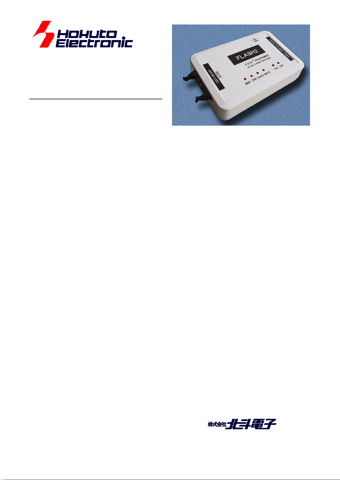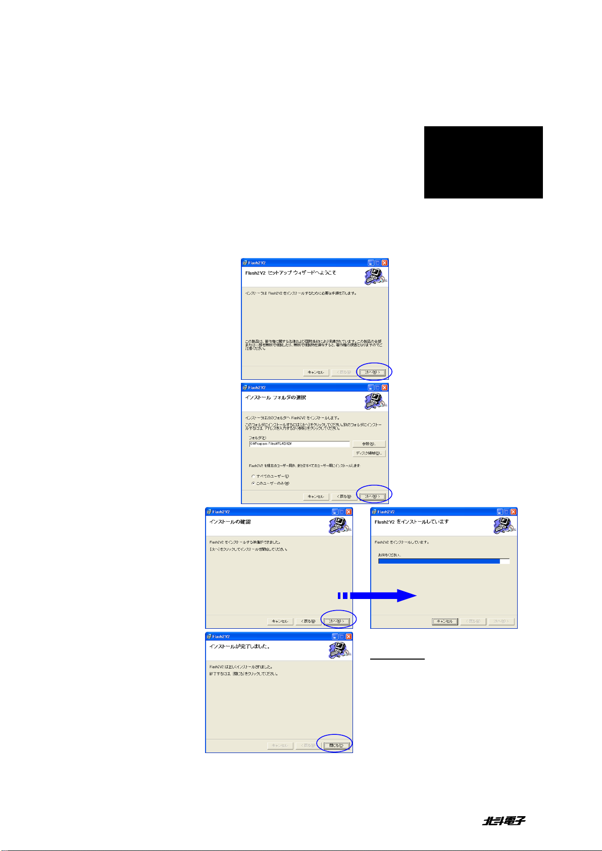
HOKUTO DENSHI CO;LTD; FLASH2 株式会社
●
IMPORTANT
MATTERS ON SAFETY
Do not use the FLASH2 before reading this user’s manual.
Make sure that you fully understood this user’s manual, before using the FLASH2 and power adapter.
Reading the manual is the responsibility of the FLASH2 users to fully understand all the matters.
THINGS OF IMPORTANCE
●The FLASH2 and attached software are products made by HokutoDenshi Co., Ltd.
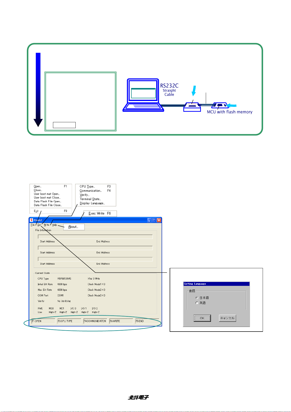
●The FLASH2 is to be used by connecting with systems containing the Renesas Electronics made MCU
with flash memory built-in microcomputer. The FLASH2 is not to be used for any other purpose other than
that which is specified in the manual.
●THE FLASH2 MUST NOT BE ALTERED IN ANY CASE.
HokutoDenshi Co., Ltd. is always improving the product design and performance. These changes will be
notified with releases of future product releases.
Users of FLASH2: Users only who have fully read and understood the manual should use the
FLASH2.Users who have not read and not fully understood the manual must not use the FLASH2.
●Possession/Ownership/Copyright: The FLASH2 described in the manual is protected by copyright and
this copyright is the property of HokutoDenshi Co., Ltd
●Product Diagrams: There may be cases where a product diagram in the manual differs from the product.
●HokutoDenshi Co., Ltd. has no responsibility for damages and dangers that may come about from
incorrect use of the FLASH2. All incorrect usage's and subsequent warnings against these usages, that
may not have been thought, are the responsibility of the users of FLASH2 who use the FLASH2 according
to the usage as is specified in the manual.
LIMITED GUARANTEE
HokutoDenshi Co., Ltd. guarantees that the FLASH2 can be used by the usage described in this manual by
HokutoDenshi Co., Ltd., and guarantees that the FLASH2 has been produced correctly and is free of any
defects per the products specification. The FLASH2 is guaranteed for 1 year after purchase of the FLASH2.
WHAT THIS GUARANTEE DOES NOT INCLUDE
●HokutoDenshi Co., Ltd. guarantees the product only when the product is used correctly as described in
the manual. This guarantee is not valid if the product is misused for purposes other than that specified in the
manual. The guarantee is valid only for the materials used to construct the product.
●HokutoDenshi Co.,Ltd accepts no responsibility for whatever costs associated directly(or indirectly) with
damaged(or faulty) goods.
●This guarantee is valid for only the original purchaser of the product.
For the damages arose cumulatively, when the guarantee explicitly covers the damages, the guarantee is
limited to received value of the product price no matter what the reasonsare.
Any application for retailing the product by a third party cannot be accepted. The purchaser of the product
assumes all responsibility after the FLASH2 purchase.
This guarantee is not valid in the following cases.
1. Fire, earthquake, flood, an accident caused by a third party, etc.
2. Incorrect use, misuse, abuses user mistake and / or use in an improper environment.
3. The product has been altered in any way or tampered with.
4. The method of use has resulted in damage to the product, or a defect with the product.
WARNINGS
Failure to adhere to the following warnings may result in possible heat, smoke and fire damage
to the FLASH2 and surrounding systems.
1. Don't disconnect and don't reconnect power cables while power is on.
2. Don't remove and don't replace any circuit while power is on.
3. Don't use power voltages other than what is specified in circuit diagram.
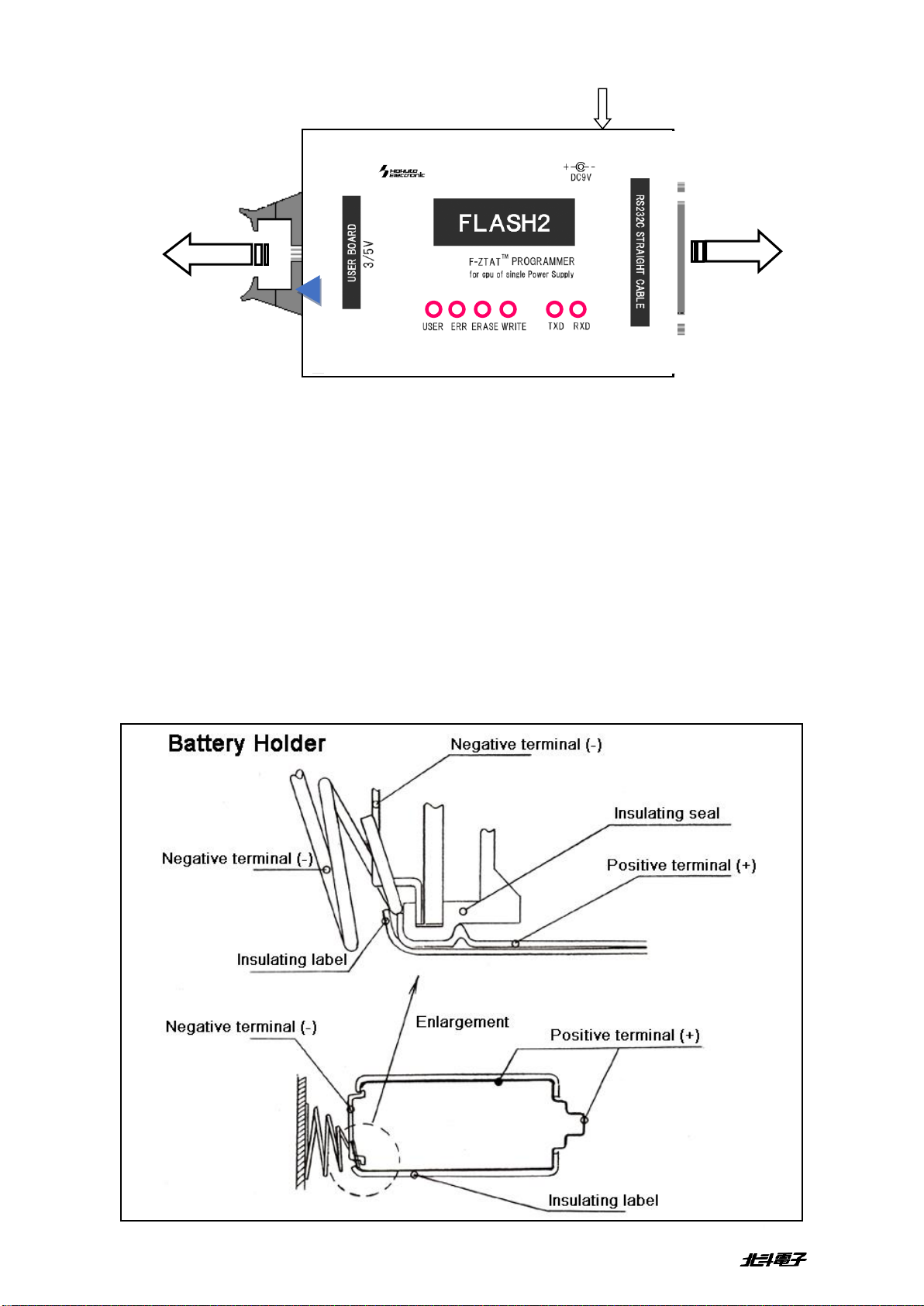
4. Be sure to use the correct connector cables when connecting between the FLASH2, MCU
and peripheral systems.