Keith & Koep MT6N User manual

Keith & Koep GmbH 21. October 2002
1von 49
MT6N (MT606)
Documentation 6.0
1.0 Introduction
The MT6N is an industrial terminal based on the Keith & Koep “Trizeps1“ module.
The board offers the following features:
•CompactFlash slot / PCMCIA adaption connector
•2 x RS232 interface (1 x DB9 male, 1 x 10-pin header)
•CAN interface (Philips SJA1000)
•Ethernet interface (SMSC LAN91C96)
•PS/2 connector (keyboard or mouse)
•Uninterruptible Power Supply (optional)
•USB target (external clamping diode, VCC necessary)
•LCD-Connector (40-pin header, included touch interface) to connect with B/W
or color DSTN, TFT; direct connection to Sharp LM8V31 (VGA DSTN)
•Audio interface (Microphone and speaker)
•2 x 8 TTL inputs, 2 x 8 TTL outputs, which can be electrically isolated on an
optional circuit board
•Connector for additional UART or IrDA
•Battery buffered Real Time Clock (RTC)
•Single power supply (24V)
1. Keith & Koep GmbH offers two kinds of Trizeps modules. First one, in the following
called „Trizeps I“, based on the Intel StrongARM SA-1110 Microprocessor. The second
one, called „Trizeps II“, based on the PXA250 Microprocessor. Both processors work
very fast (270 Dhrystone 2.1 MIPS @ 206MHz for Trizeps I and 480 Dhrystone 2.1 MIPS
@ 400MHz for Trizeps II) and need very low power. Both Trizeps modules include also
the Philips UCB 1x00 (a single chip, integrated mixed signal audio and telecom codec).
The single channel audio codec is designed for direct connection of a microphone and a
speaker. The incorporated analog to digital converter and the touch screen interface pro-
vides complete control and read-out of an 4 wire resistive touch screen. The Trizeps offers
up to 16MByte Flash memory and up to 64MByte SDRAM.

Keith & Koep GmbH Preface
MT6N (MT606) 2von 49
2.0 Preface
2.1 Getting started
The MT6N board is designed as a motherboard for Trizeps I and Trizeps II. The
first part of this chapter gives a physical description of the board and the second part
describes:
1. How to unpack the board and how to make a visual inspection.
2. How to power up the board for the first time.
3. How to connect the board to a host system
2.1.1 Physical description
The physical layout of the board is shown in figure 6 on page 23 (You’ll find details
on the last page). The dimensions of the board are 223 x 134 mm (LxW). You can
find all measures at figure 8 on page 49.
There are a number of header blocks on the board that accept 2-pin jumpers, allow-
ing the board to be configured in different ways. Due to further header blocks it is
possible to connect an LCD-display with touch screen. A serial connection to a host
system is possible by using one of the RS232 interfaces. Furthermore the board con-
tains an JTAG-interface for programming the Trizeps.
2.1.2 Unpacking the board
The MT6N contains electronic components that are susceptible to electrostatic dis-
charge (static electricity). To avoid electrostatic damage the board is supplied in an
antistatic bag. When handling the card, risk of damage can be diminished by taking
a few simple precautions:
1. Do not remove the card from the bag unless you are working on an antistatic,
grounded surface and wearing an grounded antistatic wrist strap.
2. Keep the antistatic bag the card was supplied in; if you remove the card from a
system, store it in the bag.
Normally MT6N is supplied with a Trizeps in the SODIMM-socket. If the
SODIMM is not fitted with Trizeps when you receive your board, follow the next
instructions:
1. Slide the Trizeps into the socket taking account of the polarity mark. Do not
touch the gold contacts. You can see that there is a polarization mark cut in the
Trizeps; this ensures that the Trizeps is adjusted correctly. Put the Trizeps modul
carefully at an angle of about 30 degrees into the socket.
2. Support the underside of the board and push the Trizeps down into the socket. It
should click into its place with a gentle click.
Before you install and power up your MT6, you should perform a short visual
inspection:
1. Inspect the card for physical damage.
2. Ensure that each of the 2-pin jumpers is pushed down firmly onto its mounting
posts. If you move any of the jumpers, refer to Appendix A to ensure they are
replaced correctly.

Keith & Koep GmbH Functional specification
MT6N (MT606) 3von 49
2.1.3 Powering up the first time
Use Appendix A to ensure the jumpers are set appropriately. If you need more
details on how to install the card or attach power supply, refer to Appendix A, too.
2.1.4 How to connect the board to host system
Use an RS232 null-modem cable to attach the serial interface on the board to an
RS232 port on a terminal or terminal emulator. For example, you could connect it to
a PC running Windows and use the Windows Terminal or Hyperterminal applica-
tion. Configure the terminal to operate at 38 kbaud, 8-bit data, 1 stop bit, no parity,
no flow control. If you need more details on choosing an appropriate cable, refer to
appendix A.
3.0 Functional specification
This chapter describes each functional element on the MT6N board. In the next
chapters you can find more detailed information about the board and some impor-
tant hints for programming it. The block diagram on figure 1 on page 4 shows the
interconnections of the major elements.
Components of MT6:
1. Trizeps module
2. Serial EEPROM (optional)
3. CompactFlash / PCMCIA
4. Board Control Register BCR
5. Real Time Clock
6. JTAG interface
7. Reset
8. Power Supply
9. Power generation on board
10.GPIO
11. Ethernet
12.Serial ports
13.CAN interface
14.TTL I/O
15.Audio in/out
16.Display connectors and 4 wire Touch Panel
17.MultiMediaCard
18.PS/2 interface
19.Powerfail - Interrupt
20.Uninterruptible Power Supply (UPS)

Keith & Koep GmbH Functional specification
MT6N (MT606) 4von 49
FIGURE 1. MT6 block diagram
Flash SDRAM CODEC
UCB1200
Trizeps
Display
Touchpanel
RS232
serial port 1
RS232
serial port 3
Ethernet
MMC Ext IrDA /
16 TTL
RTC
Fuse
Power +24V +12V
Regulator
Regulator
+3V3
+5V
I/O ports 10 Base-T
interface
Supply Filter
Regulator
serial port 2
CompactFlash /
PCMCIA-Adaption
serial port 4
SSP
UART
PS/2
CAN
interface
mouse or
keyboard

Keith & Koep GmbH Functional specification
MT6N (MT606) 5von 49
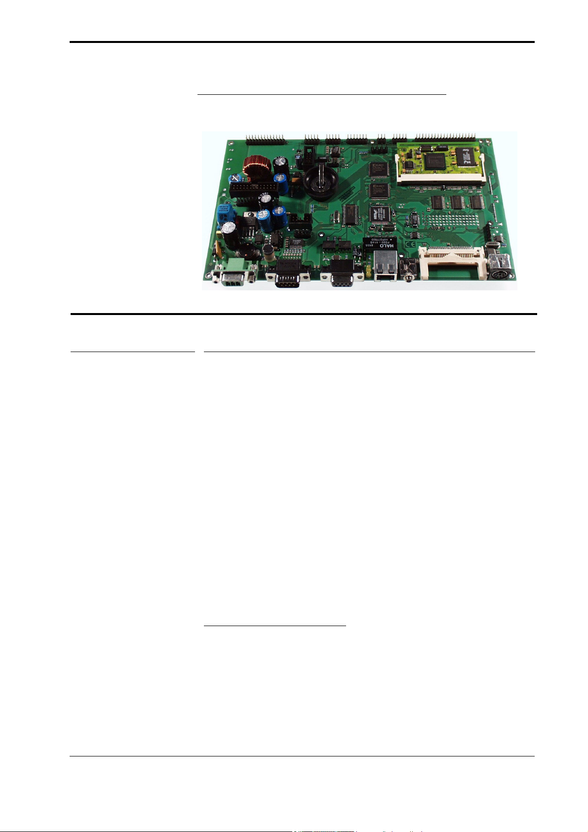
3.1 Trizeps
The MT6 board is fitted out either with the Trizeps I or the Trizeps II module.
3.1.1 Trizeps I
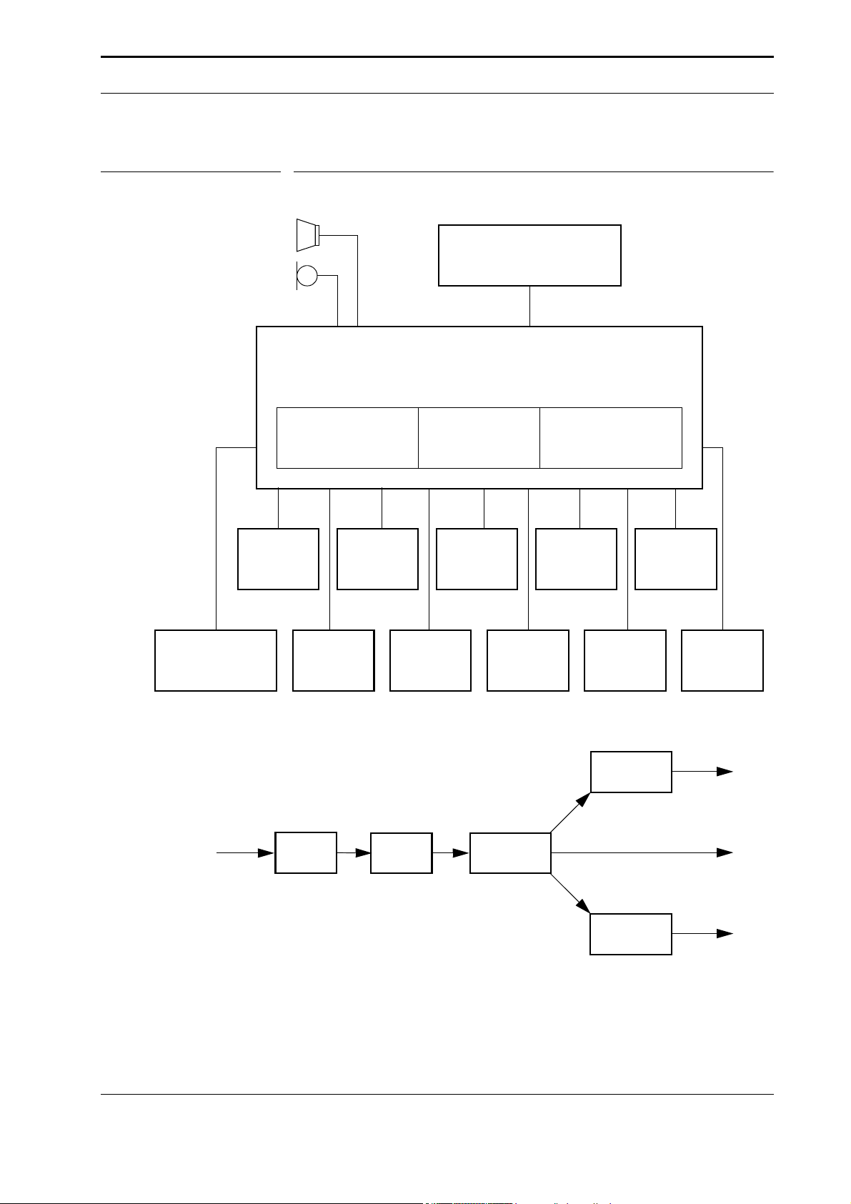
The Trizeps board is based on the Intel StrongArm SA-1110 Microprocessor - a
highly integrated communications microcontroller that incorporates a 32-bit Strong-
Arm Risc Processor core, system support logic, multiple communication channels,
an LCD controller, a memory and PCMCIA controller, and general-purpose I/O
ports.The SA-1110 is working very fast (150 Dhrystone 2.1 MIPS @ 133 MHz or
235 Dhrystone 2.1 MIPS @ 206 MHz) and needs very low power. Trizeps includes
also the Philips UCB 1200 (a single chip, integrated mixed signal audio and telecom
codec). The single channel audio codec is designed for direct connection of a micro-
phone and a speaker. The built-in telecom codec can directly be connected to a
DAA and supports high speed modem protocols. The incorporated analog to digital
converter and the touch screen interface provides complete control and read-out of
an 4 wire resistive touch screen.
3.1.2 Trizeps II
The Trizeps II Module is based on the Intel® XScale™ core-based CPU (200, 300
and 400 MHz) PXA250 - ARM Architecture v.5TE compliant and application code
compatible with Intel® SA-1110 processor which is used on the Trizeps I module.
The CPU based on Intel® Superpipelined RISC technology utilizing advanced Intel
0.18µ process for high core speeds at low power (480K Dhrystone 2.1 per second
@ 400 MHz). Some features of the XScale: Integrated memory and PCMCIA/Com-
pactFlash Controller with 100MHz Memory Bus, 16-bit or 32-bit ROM/Flash/
SRAM six banks, 16-bit or 32-bit SDRAM; System Control Module includes 17
dedicated general-purpose interruptible I/O ports, real-time clock, watchdog and
interval timers, power management controller, interrupt and reset controller, LCD
controller and two on-chip oscillators. Trizeps-II includes also the Philips UCB
1400, on a single chip it combines audio codec functions, a touch-screen controller
and power management interfaces. The incorporated A/D converter and the touch
screen interface provides complete control and read-out of a 4 wire resistive touch
screen.
3.2 Serial EEPROM (optional)
MT6N provides a serial EEPROM (X24C16- Xicor) to be used as a non-volatile
memory. It has a size of 16KBit and it is internal organized as 2048 x 8. The
X24C16 offers a serial interface and a software protocol allowing operation on a
simple two wire bus with I2C_CLK (GPIO26 of SA-1110) and I2C_DATA (GPIO27
of SA-1110). The EEPROM is optional and usually not placed.
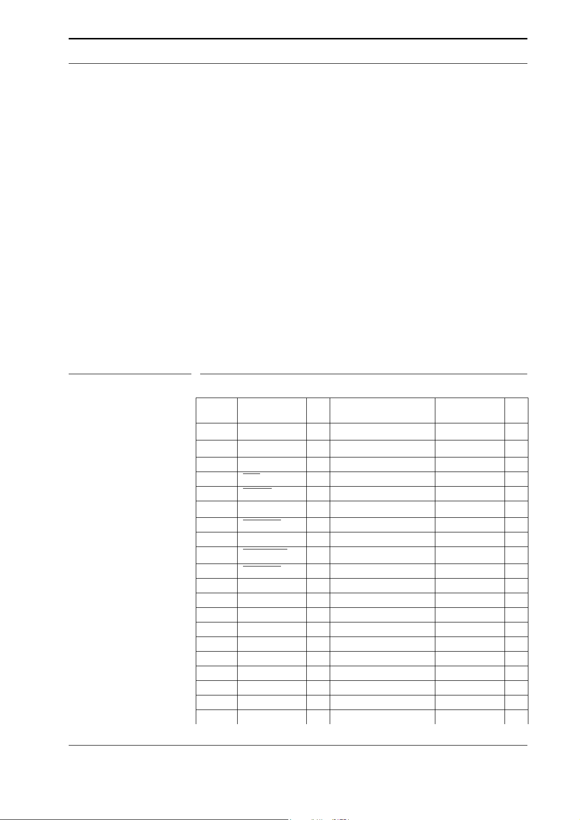
FIGURE 2. The slave address of the EEPROM:
•Read address: A1
•Write address: A0
1010000R/W
Device Type
Identifier
High order
word address

Keith & Koep GmbH Functional specification
MT6N (MT606) 6von 49
3.3 CompactFlash / PCMCIA
The MT6N is delivered with a Type I CompactFlash connector. In addition
(optional) there is a 68-leaded adaption connector which carries all signals for a sin-
gle Type II PCMCIA-Slot connector.
3.3.1 PCMCIA
In the past memory expansion cards (specification 1.0) of the size of check cards
had just the purpose of providing memory. With the today generally valid specifica-
tion 2.0 much of I/O units can be placed in a PCMCIA-slot. This includes for exam-
ple SCSI-adaptation, Ethernet-Card or modem cards.
The PCMCIA-adaption connector on the board is designed on the basis of specifi-
cation 2.0 (representative of this specification is the Personal Computer Memory
Card International Association)
The adjustment of the supply voltage and the programming voltage of the PCM-
CIA-card is to be effected by the Board Control Register.
3.3.2 CompactFlash
CompactFlash is a very small removable mass storage device. It provides complete
PCMCIA-ATA functionality and compatibility plus TrueIDE functionality compati-
ble with ATA/ATAPI-4. At 43mm (1.7“) x 36mm (1.4“) x 3.3mm (0.13“), the
device’s thickness is less than one-half of a current PCMCIA Type II card. It is actu-
ally one-fourth the volume of a PCMCIA card. Compared to a 68-pin PCMCIA
card, a CompactFlash card has 50 pins (the connector is similar to the PCMCIA
card) but still conforms to PCMCIA-ATA specs. CompactFlash cards are designed
with flash technology, a non-volatile storage solution that does not require a battery
to retain data indefinitely. CompactFlash storage products are solid state, meaning
TABLE 1. PCMCIA and CF Status Register
Offset 0x00000000 PCMCIA Status Register
Bit 15 14 13 12 11 10 9 8 7 6 5 4 3 2 1 0
Reserved
VS[1.0]
BVD[1:0]
Bits Name Type Description
1:0 BVD[2..1] Read Only
Charge Condition of PC-card
00 - Battery low, data loss
01 - Warning, battery must be chan-
ged, but no data loss till now
10 - Battery low, data loss
11 - Battery OK
3:2 VS[2:1] Read Only
Voltage Sense lines
xxa- 5V operation
0x - 3V3 operation
a. x means unconnected

Keith & Koep GmbH Functional specification
MT6N (MT606) 7von 49
they contain no moving parts, and provide users with much greater protection of
their data than conventional magnetic disk drives.
3.4 Board Control Register BCR
The MT6N board requires additional GPIO output functions, which are imple-
mented in the Board Control Register (BCR) to control the Compact Flash, PCM-
CIA, display and something else.
The PCMCIA-Switcher (MIC2562a-1) can be adjusted by the data lines D00 to
D03. The MIC2562a-1 switches between the three power supplies (0V, 3.3V and
TABLE 2. Board Control Register
Offset 0x02000000 Board Control Register
Bit 1514131211109876543210
Reset ????????00100000
Reserved
PCMCIA_RESET
FORCE_ON
PCMCIA_BUF_EN
L_DISP
CONTR_LOGIC
[3..0]
Bits Name Type Description
3:0
CONTR_
LOGIC
[3..0]
Write Only
PCMCIA Power Control Logic
see table 3 on page 8
4 L_DISP Write Only
Display enable
0 - Display off
1 - Display on
5PCMCIA_
BUF_EN Write Only
PCMCIA buffer enable
0 - PCMCIA buffer enable ON
1 - PCMCIA buffer enable OFF
6FORCE_
ON Write Only
Turn on RS232 tranceiver
0 - RS232 transceiver OFF
1 - RS232 transceiver ON
7PCMCIA_
RESET Write Only
Resetting PCMCIA card
0 - Normal operation
1 - Resetting PCMCIA

Keith & Koep GmbH Functional specification
MT6N (MT606) 8von 49
5.0V) and the programming voltages (OFF, 0V, 3.3V, 5.0V or 12.0V), which are
needed for the PCMCIA-cards.
With setting the data bus D04 the display control signal L_DISP can be switched.
The important thing about that is the power on/off timing of the display. Usually the
correct sequence is as followed:
1. Power Supply
2. Input signal
3. Contrast voltage
4. Display control signal L_DISP
If you use another display as delivered from Keith & Koep you should test the cor-
rectness of the power on/off sequences.
Resetting the data bus D05 switches the address and control-signals of the PCM-
CIA-buffer.
With setting the data bus D06 the serial interface driver is switched on.
With setting the data bus D07 a reset-signal is sent to the PCMCIA-slot.
TABLE 3. MIC2562a-1 Control Logic Table
D00 D01 D02 D03 Vcc out Vpp out
0000ClampedtoGround Clamped to Ground
0001ClampedtoGround High Z
0010ClampedtoGround High Z
0011ClampedtoGround High Z
01005V ClampedtoGround
01015V 5V
01105V 12V
01115V HighZ
10003.3V ClampedtoGround
10013.3V 3.3V
10103.3V 12V
10113.3V HighZ
1100ClampedtoGround Clamped to Ground
1101ClampedtoGround High Z
1110ClampedtoGround High Z
1111ClampedtoGround High Z

Keith & Koep GmbH Functional specification
MT6N (MT606) 9von 49
3.5 Real Time Clock (RTC)
MT6N contains a Low-Power RTC from Philips, called PCF8593. This chip uses
the same two wire bus as the serial EEPROM, which is described in figure 2 on
page 5.
FIGURE 3. The slave address of the RTC
Read address: A3
Write address: A2
The RTC is either supplied from the onboard battery or from an external battery.
3.6 JTAG interfaces
The SA-1110 contains a JTAG port that allows test access to the I/O pins of the
device. The JTAG port is designed as a 10-pin header connector.
With a second JTAG interface program the CPLDs on board. It is designed as a 6-
pin header.
3.7 Reset
There are two sources of reset on the MT6N:
1. Power-on Reset
2. Reset from the watchdog timer
Power-on reset is generated automatically when power is applied to the board. It
can also be initiated by a push button switch attached to a 2-pole 0.1-inch pitch con-
nector on the board.
Resets generated by any of these methods are equivalent and indistinguishable.
3.8 Power Supply
Power supply is possible on several ways:
First: The Power supply of MT6N is accessible by a power connector by Phoenix
with part number PSC 1,5/3-M. Pin 1 is the positive one (+24V) and Pin 3 is
Ground.
Second: It is also possible to supply MT6N by an optional PCB where the TTL I/O
ports are electrically isolated. More information: http://www.keith-koep.com.
Third: Supply through a 2-pin connector by Phoenix, which is optional and usually
not placed.
1110000R/W
Device Type
Identifier
High order
word address

Keith & Koep GmbH Functional specification
MT6N (MT606) 10 von 49
3.9 Power generation on board
+12V are generated from the +24V power supply using a DC-DC converter. This
voltage is just needed for some PCMCIA cards and for some kinds of backlight
inverter of the display.
The power supplies +5V and +3V3 are generated from the +12V power by two fur-
ther DC-DC converters. The +5V are used by PCMCIA or CompactFlash cards,
CAN and for backlight inverter. The +3V3 are used by Trizeps, Ethernet, PCMCIA
or CompactFlash cards, serial interfaces and something else.
3.10 GPIO
Both (Trizeps I and Trizeps II) modules put GPIOs at free disposal.
3.10.1 GPIO (Trizeps I)
The SA-1110 provides 28 general purpose I/O port pins for use in generating and
capturing application specific input and output signals. Each pin is programmable
as an input or output and as an interrupt source. Most GPIO pins have an alternate
function which can be invoked to enable additional functionality within the SA-
1110. If a GPIO is used for this alternate function it cannot be used as a GPIO at the
same time. The table below shows each GPIO pin with the using on MT6N and its
corresponding alternate function.
TABLE 4. GPIOs of SA1110 (Trizeps I) used on MT6 and their alternate functions
SA1110
Pin
Function on
MT6 Dir Description
Alternate
function Dir
GP[27] I2C_DATAabi Data I2C-bus 32KHZ_OUT out
GP[26] I2C_CLKbout Clock I2C-bus RCLK_OUT out
GP[25] ANGELBOOT in Start of angel BSL RTC Clock out
GP[24] PCD in PCMCIA card detect Reserved
GP[23] IRQ_IO in Interrupt of TTL I/O TREQB in
GP[22] IRQ_CODECcin Interrupt of UCB1200 TREQA in
GP[21] IRQ_CAN in Interrupt of CAN TIC_ACK out
GP[21] MCP_CLK in
GP[20] INVALID_3 in RS232-Invalid-signal (3)dUART_SCLK3 in
GP[19] IRQ_SMC in Interrupt of Ethernet SSP_CLK in
GP[18] DCD_3 in Data carrier detect (3) UART_SCLK1 in
GP[17] DSR_3 in Data set ready (3) SDLC_AAF out
GP[16] DTR_3 out Data terminal ready (3) SDLC_SCLK bi
GP[15] CTS_3 in Clear to send (3) UART_RXD in
GP[14] RTS_3 out Request to send (3) UART_TXD out
GP[13] CTS_1 in Clear to send (1) SPI_CS out
GP[12] RTS_1 out Request to send (1) SPI_CLK out
GP[11] SPI_RXD in in
GP[10] SPI_TXD out out
GP[2-9] LDD[8-15] out Display signal LDD[8-15] out

Keith & Koep GmbH Functional specification
MT6N (MT606) 11 von 49
3.10.2 GPIO (Trizeps II)
The PXA250 processor enables and controls its 81 general purpose I/O (GPIO) pins
through the use of 27 registers which configure the pin direction (input or output),
pin function, pin state (outputs only), pin level detection (inputs only), and selection
of alternate functions. The PXA250 processor provides 81 GPIO pins for use in
generating and capturing application specific input and output signals. Each pin can
be programmed as either an input or output.When programmed to be an input, a
GPIO can also serve as an interrupt source. If a GPIO is used for it alternate func-
tion it cannot be used as a GPIO at the same time. The table below shows each
GPIO pin with the using on MT6N and its corresponding alternate function.
GP[1] PRDY in Interrupt PCMCIA Reserved
GP[0] IRQ_PIC in Interrupt PIC Reserved
a. 100K pulled up
b. 100K pulled up
c. Used on Trizeps internally
d. The number in parenthesis named the serial port
TABLE 5. GPIOs of PXA250 (Trizeps II) used on MT6 and their alternate functions
PXA250
Pin
Function on
MT6 Dir Description
Alternate
function
Di
r
GP[80] CS[4] out Active low chip select 4 nCS[4] out
GP[79] CS[3] out Active low chip select 3 nCS[3] out
GP[78] CS[2] out Active low chip select 2 nCS[2] out
GP[77] L_BIAS out LCD AC BIAS LCD_ACBIAS out
GP[76] L_PCLK out LCD pixel clock LCD_PCLK out
GP[75] L_LCLK out LCD line clock LCD_LCLK out
GP[74] L_FCLK out LCD frame clock LCD_FCLK out
GP[73] LDD15 out LCD data pin 15 LDD[15] out
GP[73] Memory controller grant MBGNT out
GP[72] LDD14 out LCD data pin 14 LDD[14] out
GP[72] 32 KHz clock 32 kHz out
GP[71] LDD13 out LCD data pin 13 LDD[13] out
GP[71] 3.6 MHz oscillator clock 3.6 MHz out
GP[70] LDD12 out LCD data pin 12 LDD[12] out
GP[70] Real Time Clock (1Hz) RTCCLK out
GP[69] LDD11 out LCD data pin 11 LDD[11] out
GP[69] MMC_CLK MMCCLK out
GP[68] LDD10 out LCD data pin 10 LDD[10] out
GP[68] MMC Chip Select 1 MMCCS1 out
TABLE 4. GPIOs of SA1110 (Trizeps I) used on MT6 and their alternate functions
SA1110
Pin
Function on
MT6 Dir Description
Alternate
function Dir

Keith & Koep GmbH Functional specification
MT6N (MT606) 12 von 49
GP[67] LDD09 out LCD data pin 9 LDD[9] out
GP[67] MMC Chip Select 0 MMCCS0 out
GP[66] LDD08 out LCD data pin 8 LDD[8] out
GP[66] MBREQ MBREQ in
GP[58]-
GP[65]
LDD[00-07] out LCD data pin 0 to7 LDD[0-7] out
GP[57] PIOIS16 in Bus Width select I/O card nIOIS16 in
GP[56] PWAIT in Wait signal for card space nPWAIT in
GP[55] PREG out Card address bit 26 nPREG out
GP[54] PSKTSEL out Socket select for card space PSKTSEL out
GP[54] MMC Clock MMCCLK out
GP[53] PCE2 out Card Enable for card space nPCE[2] out
GP[53] MMC Clock MMCCLK out
GP[52] PCE1 out Card Enable for card space nPCE[1] out
GP[51] PIOW out I/O Write for Card space nPIOW out
GP[50] PIOR out I/O Read for Card space nPIOR out
GP[49] PWE out Write enable for card space nPWE out
GP[48] POE out Output Enable for card space nPOE out
GP[47] TXD_2 out STD_UART transmit data TXD out
GP[47] ICP transmit data ICP_TXD out
GP[46] RXD_2 in STD_UART receive data RXD in
GP[46] ICP receive data ICP_RXD in
GP[45] BT_RTS out BTUART request to send RTS out
GP[44] BT_CTS in BTUART clear to send CTS in
GP[43] BT_TXD out BTUART transmit data BTTXD out
GP[42] BT_RXD in BTUART receive data BTRXD in
GP[41] FF_RTS out FFUART request to send RTS out
GP[40] FF_DTR out FFUART data terminal ready DTR out
GP[39] FF_TXD out FFUART transmit data FFTXD out
GP[39] MMC Chip select 1 MMCCS1 out
GP[38] FF_RI in FFUART ring indicator RI in
GP[37] FF_DSR in FFUART data set ready DSR in
GP[36] FF_DCD in FFUART data carrier detect DCD in
GP[35] FF_CTS in FFUART clear to send CTS in
GP[34] FF_RXD in FFUART receive data FFRXD in
GP[34] MMC chip select 0 MMCCS0 out
GP[33] CS5 out Active low chip select 5 nCS[5] out
GP[32] AC97 Sdata_in1 SDATA_IN1 in
GP[31] AC97SYNCaout AC97 sync SYNC out
TABLE 5. GPIOs of PXA250 (Trizeps II) used on MT6 and their alternate functions
PXA250
Pin
Function on
MT6 Dir Description
Alternate
function
Di
r

Keith & Koep GmbH Functional specification
MT6N (MT606) 13 von 49
GP[31] I2S sync SYNC out
GP[30] AC97DOUTaout AC97 Sdata_out SDATA_OUT out
GP[30] I2S Sdata_out SDATA_OUT out
GP[29] AC97DINain AC97 Sdata_in0 SDATA_IN0 in
GP[29] I2S Sdata_in SDATA_IN in
GP[28] BITCLKain AC97 bit_clk BITCLK in
GP[28] I2S bit_clk BITCLK in
GP[28] I2S bit_clk BITCLK out
GP[27] EXT_CLK in
GP[26] RXD in
GP[25] PWR_FAIL in Powerfail IRQ TXD out
GP[24] PCD in PCMCIA card detect SFRM out
GP[23] IRQ_IO in TTL I/O IRQ SCLK out
GP[22]
GP[21] IRQ_CAN in CAN IRQ
GP[20] INVALID_3 in RS232 Invalid signal DREQ[0] in
GP[19] IRQ_SMC in Ethernet IRQ DREQ[1] in
GP[18] RDY in External bus ready RDY in
GP[17] PWM1 output PWM1 out
GP[16] PWM0 output PWM0 out
GP[15] CS1 out Active low chip select 1 nCS[1] out
GP[14] Memory bus master request MBREQ in
GP[13] Memory controller grant MBGNT out
GP[12] 32 kHz out 32 kHz out
GP[11] 3.6 MHz oscillator out 3.6 MHz out
GP[10] Real time clock (1Hz) RTCCLK out
GP[9] MMC Chip select 1 MMCCS1 out
GP[8] MMC Chip select 0 MMCCS0 out
GP[7] 48 MHz clock output 48 MHz clock out
GP[6] MMC clock MMCCLK out
GP[5]
GP[4]
GP[3]
GP[2] IRQ_CODECain UCB1x00 IRQ
GP[1] PRDY in PCMCIA IRQ GP_RST in
GP[0] IRQ_PIC in PIC IRQ
a. used on Trizeps II internally
TABLE 5. GPIOs of PXA250 (Trizeps II) used on MT6 and their alternate functions
PXA250
Pin
Function on
MT6 Dir Description
Alternate
function
Di
r

Keith & Koep GmbH Functional specification
MT6N (MT606) 14 von 49
3.11 Ethernet
The Ethernet Controller (LAN91C96 by SMSC) on the MT6N board supports the
IEEE 802.3 (ANSI 8802-3) Ethernet Standards. It is connected to a 10 Base-T filter
module. The Ethernet connector is of the type RJ45. The controller in the configura-
tion of MT6N provides:
•6K Bytes of On-Chip RAM
•Support of enhanced transmit queue management
•Direct interface to ISA buses with no wait states
•Fast access time (40ns)
•Pipelined data path
•Integrated 10Base-T Transceiver functions:
•Driver and receiver
•Link integrity test
•Receive polarity detection and correction
•10 Mb/s Manchester Encoding / Decoding and clock recovery
•Automatic retransmission, bad packet rejection and transmit padding
•Optional configuration via serial EEPROM interface (jumperless)
•Two direct driven LEDs for diagnostics (transmit / receive indication)
3.12 Serial ports
The MT6 provides four kinds of serial ports:
•USB
•UART
•IrDA
•SPI
3.12.1 Serial port 0 - USB Device Controller
Serial port 0 is an universal serial bus device controller (UDC) that supports three
endpoints and can operate half-duplex at a baud rate of 12 Mbps (slave only, not a
host or hub controller).The UDC is USB-compliant and supports all standard device
requests is issued by the host. The external pins dedicated to this interface are
UDC+ and UDC-. The USB protocol uses differential signalling between the two
pins for half-duplex data transmission. A 1.5 KOhm pull-up resistor is connected to
the USB cable’s D+ signal to pull the UDC+ pin high when not driven. This signi-
fies the UDC is a high-speed, 12 Mbps device and provides the correct polarity for
data transmission.
Serial port 0 is accessible by an SL1-4 (four pin header). However, the user should
refer to the Universal Serial Bus Specification, Revision 1.01for a full description
of the USB protocol and its operation.
3.12.2 Serial port 1 - UART
Serial port 1 is configured as an universal asynchronous receiver / transmitter
(UART) serial controller. A Maxim MAX3223 RS232 transceiver is used to man-
age the level conversion and line interface. The device has a power saving auto-
1. The latest revision of the Universal Serial Bus Specification Revision 1.0 can be accessed
via the World Wide Web Internet side at: http://www.teleport.com/~usb/

Keith & Koep GmbH Functional specification
MT6N (MT606) 15 von 49
matic shutdown that powers down the chip if no valid RS232 levels are detected.
The component may also be forced off by the FORCEON signal. Serial port 1 is
accessible by the female serial port connector J18 (10-pin header). The external pins
dedicated to this interface are TXD1 and RXD1. Further GPIO 12 and 13 are used
as hand-shake signals RTS and CTS.
For the communication between the PC (DB9 male) and the MT6 a serial extension
cable is needed. Therefore the serial port J18 (10 pin header) is to be connected with
a short flat cable to a DB9 female connector (see figure 7 on page 36).
3.12.3 Serial port 2 - Infrared communications port
The infrared communications port (ICP) operates at half-duplex and provides direct
connection to commercially available Infrared Data Association (IrDA) compliant
LED transceivers. The ICP supports both the original IrDA standard with speeds up
to 115.2 Kbps as well as the newer 4-Mbps standard. Both standards use different
bit encoding techniques and serial packet formats. Low-speed IrDA transmission
uses the Hewlett-Packard Serial Infrared standard (HP-SIR) for bit encoding and an
UART as the serial engine; high-speed uses Four-Position Pulse Modulation
(4PPM) and a specialized serial packet protocol developed expressly for IrDA
transmission. Serial port 2 is accessible by a 10-pin header. The external pins dedi-
cated to the ICP are TXD2 and RXD2.
FIGURE 4. Sample: Use of IrDA

Keith & Koep GmbH Functional specification
MT6N (MT606) 16 von 49
Alternately you can use serial port 2 as an UART.
3.12.4 Serial port 3 - UART
Serial port 3 is configured as an universal asynchronous receiver / transmitter
(UART) serial controller. A Maxim MAX3243 RS232 transceiver is used to
manage the level conversion and line interface. The device has a power saving auto-
matic shutdown that powers down the chip if no valid RS232 levels are detected.
The component may also be forced off by the FORCEON signal. Serial port 3 is
accessible by the male serial port connector J12 (DSUB9M). This port provides
RTS, CTS, DSR, DTR and DCD modem signals to support a serial IO port PC syn-
chronous application.
3.12.5 Serial port 4 - SSP
The synchronous serial port (SSP) of the SA-1110 is used to interface to a variety of
analog-to-digital converters, audio and telecom codecs, memory chips, and keypad
controllers as well as other miscellaneous serial devices. The SSP supports the
National Microwire and Texas Instruments synchronous serial protocols as well as a
subset of the Motorola serial peripheral interface (SPI) protocol. Serial port 4 con-
trols full-duplex synchronous serial transfer between the SA-1110 and off-chip
devices. The SSP functions as a master only and communicates to the off-chip slave
device by driving a serial bit rate clock ranging from 7.2 KHz to 1.8432 MHz along
with a frame synchronisation pulse to denote the start of each frame transfer, and
supports any data format between 4 and 16 bits. The external pins dedicated to this
interface are GPIO 10 to 13.
TABLE 6. IrDA Control Register
Offset 0x02400000 IrDA Control Register
Bit 1514131211109876543210
Reset ??????????????01
Reserved
IRDA_MODE
IRDA_SD
Bits Name Type Description
0 IRDA_SD Write Only
IrDA Shutdown
0 - IrDA activ
1 - IrDA inactiv
1IRDA_
MODE Write Only
IrDA Mode
0 - Low speed
1 - High speed

Keith & Koep GmbH Functional specification
MT6N (MT606) 17 von 49
3.13 CAN interface
The CAN (Controller Area Network) is a serial bus system especially suited for net-
working “intelligent“ devices as well as sensors and actuators within a system or
subsystem. MT6 uses the SJA1000, a stand-alone CAN controller made by Philips.
It is used within automotive and general industrial environments. SJA1000 is the
successor of the PCA82C200 CAN controller (BasicCAN) from Philips Semicon-
ductors. Additionally, a new mode of operation is implemented (PeliCAN) which
supports the CAN 2.0B protocol specification with several new features.
This controller offers the following features:
•PIN and Electrical compatibility to the PCA82C200 stand-alone CAN controller
•PCA82C200 mode (BasicCan mode is default)
•Extended receive buffer (64-byte FIFO)
•CAN 2.0B protocol compatibility
•Supports 11-bit identifier as well as 29-bit identifier
•Bit rates up to 1Mbits/s
•PeliCAN mode extensions:
•Error counters with read/write access
•Programmable error warning limit
•Last error code register
•Error interrupt for each CAN-bus error
•Arbitration lost interrupt with detailed bit position
•Single-shot transmission (no re-transmission)
•Listen only mode (no acknowledge, no active error flags)
•Hot plugging support (software driven bit rate detection)
•Acceptance filter extension (4-byte code, 4-byte mask)
•Reception of ’own’ messages (self reception request)
To use the can interface, please refer to the pinout description of the can connector
(J3 DB9 female) in table 12 on page 25.
3.14 TTL I/O
MT6 offers 16 TTL Inputs and 16 TTL Outputs. There are 2 I/O connectors called
J15 and J16 on the board. Both connectors comprise each 8 TTL Input ports and 8
TTL Output ports. The pinout is shown in table 24 on page 33 and table 25 on
page 34. The output signals (OUTPUT[00:15]) correspond with dataline signals
D[00:15], which are switched by a CPLD. They will be selected by addressing
0x19800000 (\CS_IO_OUT and \CS_IO_IN). The Inputs can be read as follows:
read = *(short *) ADR
The Outputs can be written as follows:
*(short *) portadr = value
Keith & Koep GmbH offers an optional circuit board with electrically isolated
ports, one which can be placed directly on J15 and another one that will be con-
nected by a flat cable to J16. With this board it is possible to provide +24V for the

Keith & Koep GmbH Functional specification
MT6N (MT606) 18 von 49
MT6. You’ll find more information about the I/O board on our homepage
(www.keith-koep.com/trizeps.html)
3.15 Audio In/Out
The Trizeps board includes a single chip integrated mixed signal audio and telecom
codec (Philips UCB 1200). JJ2 and JJ3 on the MT6 give access to the speaker and
microphone signals. The pinout of JJ2 is shown in table 34 on page 39 and of JJ3 in
table 35 on page 39.
From MT6 Version 5 the board can be fitted out with an audio stereo connector.
3.16 Display connector and 4 wire Touch Panel
The SA-1110 on the Trizeps offers a 16 bit LCD-controller. The audio and telecom
codec (see chapter 3.15, "Audio In/Out" on page 18) provides also a 4 wire touch
screen interface. The relevant signals are accessible at J14 see table 23 on page 32.
The contrast voltage can be adjusted by an Digitally-Controlled Potentiometer by
Xicor. The device consists of a resistor array, wiper switches, a control section, and
nonvolatile memory. The wiper position is controlled by a three-wire interface.
The potentiometer is implemented by a resistor array composed of 99 resistive ele-
ments and a wiper switching network. Between each element and at either end are
tap points accessible to the wiper terminal. The position of the wiper element is con-
trolled by the CS, U/D, and INC inputs. The position of the wiper can be stored in
nonvolatile memory and then be recalled upon a subsequent power-up operation.
3.17 MultiMediaCard
The MultiMediaCard standard grew out of a joint development between SanDisk
Corporation and Siemens AG/Infineon Technologies AG, and was introduced in
TABLE 7. Display Contrast Register
Offset 0x03800000 Display Contrast Register
Bit 1514131211109876543210
Reset ??????????????11
Reserved
EEPOT_U_D
EEPOT_INC
EEPOT_CS
Bits Name Type Description
0EEPOT_
CS Write Only
Chip Select of EEPOT
0 - activ
1 - inactiv
1EEPOT_
INC Write Only
Increment of EEPOT
0 - increment by 1
1 - inactive
2EEPOT_
U_D Write Only
Direction (Up/Down)of EEPOT
0 - decrement
1 - increment

Keith & Koep GmbH Functional specification
MT6N (MT606) 19 von 49
November 1997. MultiMediaCards weigh less than two grams and, about the size of
a postage stamp, are the world’s smallest (24mm x 32mm x 1.4 mm) removable
solid-state memory solutions for mobile applications. These convenient, reliable,
rugged and lightweight standardized data carriers store up to 64 MBytes.
MultiMediaCards use ROM technology for read-only applications and Flash tech-
nology for read/write applications. The cards are fast for excellent system perfor-
mance; energy efficient for prolonged battery life in portable products; and cost-
efficient for use in systems sold at consumer price points. The simple molded pack-
age has a seven pad (pin) serial interface. This easy-to-install simple serial interface
offers easy integration into various devices regardless of the microprocessor used.
The MultiMediaCard has a wide variety of uses in some of the most exciting prod-
ucts on the market today.
3.18 PS/2 connector
The MT6 is fitted out with an PS/2 connector which allows the use of a keyboard or
a mouse.
3.19 Powerfail - Interrupt
Falling down power supply under ~14V generates an interrupt GPIO25 (Powerfail-
IRQ).
3.20 Uninterruptible Power Supply (UPS)
The easiest way to get an UPS is to use the following electrical circuit.
FIGURE 5. UPS
You can use connector J23 to supply this circuit with +12V and Ground.
This circuit is able to supply the MT6 with Trizeps in case of Powerfail for 15 sec-
onds.
C
RRRRR
CCCC
+++++
R
V
DD
+12V
GND
Values:
R: 22K
Ω
RV: 10
Ω
C: 10F / 2,3V (UltraCap by EPCOS)
D: 1N5819
(Power resistor)

Keith & Koep GmbH Functional specification
MT6N (MT606) 20 von 49
TABLE 8. UPS Register
Offset 0x02800000 UPS Register
Bit 1514131211109876543210
Reset ???????????01100
Reserved
BATT_EMPTY
AUTO_DSPL_OFF
AUTO_PWR_OFF
CHARGE
BATT_EN
Bits Name Type Description
0 BATT_EN Output
R/W
External battery enable signal
0 - external battery OFF
1 - external battery ON
1 CHARGE Output
R/W
Charge external battery
0 - Do not charge
1 - Charge
2AUTO_
PWR_OFF
Flag
R/W
Turn off system flag
0 - OS does not power down after
powerfail-IRQ
1 - OS powers down after power-
fail-IRQ
3
AUTO_
DISPL_
OFF
Flag
R/W
Turn off backlight inverter flag
0 - Leave backlight ON
1 - Powerfail-IRQ handler swit-
ches backlight OFF
4BATT_
EMPTY
Input
Read Only
External battery status
0 - External battery empty
1 - External battery full
This manual suits for next models
1
Table of contents