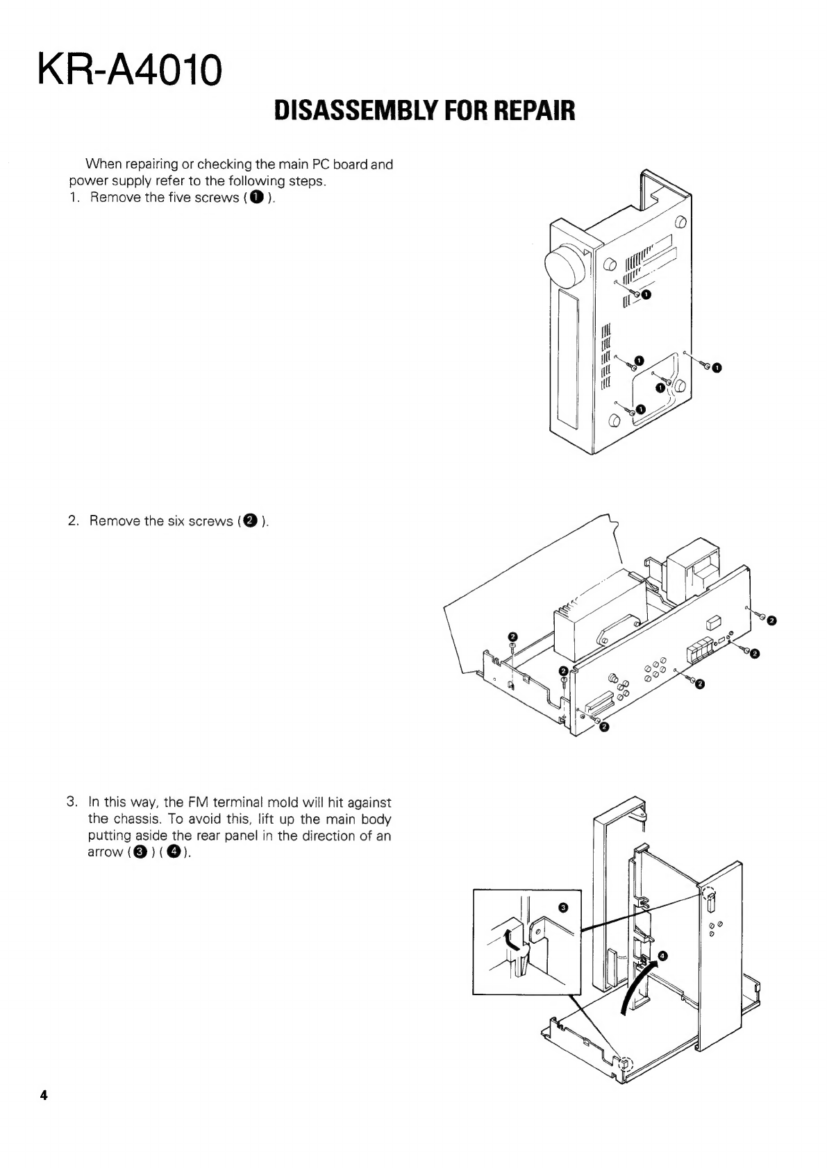
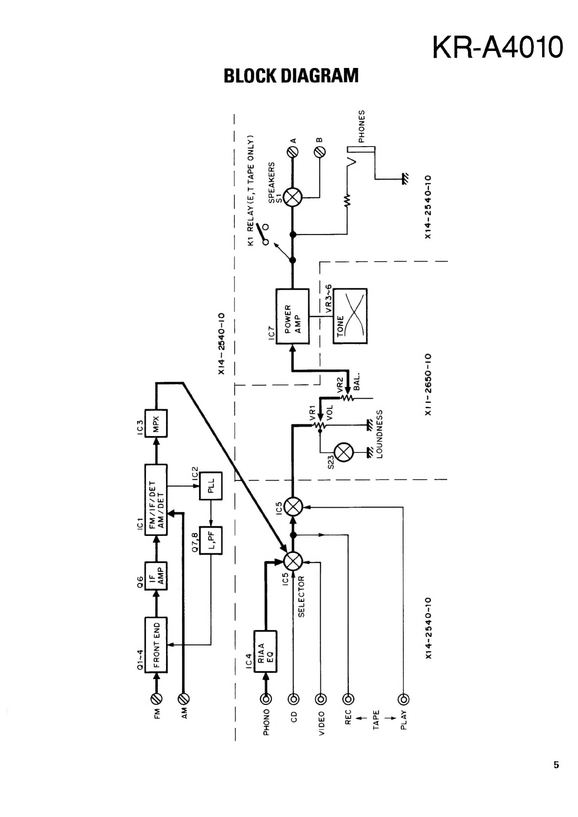
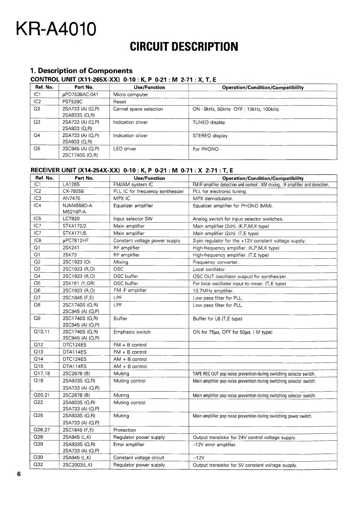
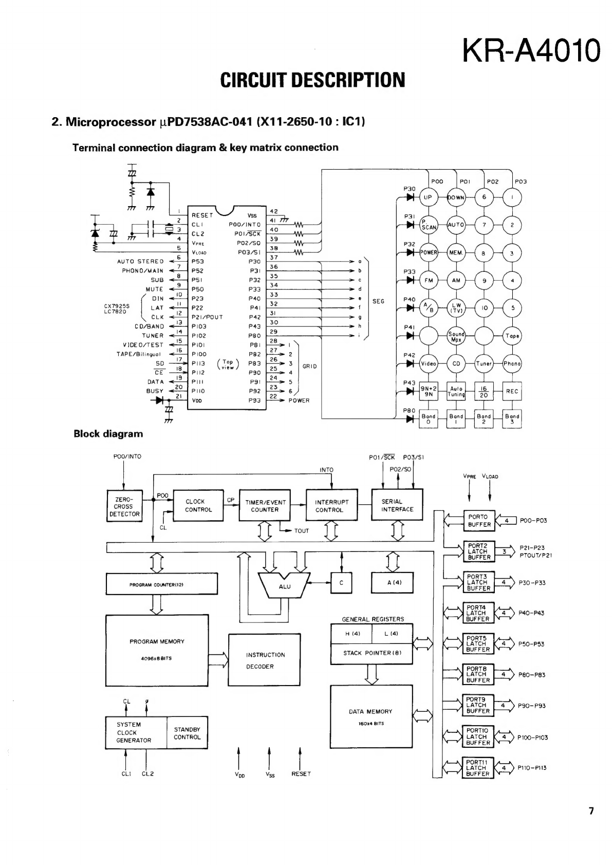
Kenwood KR-A4010 User manual

AM/FM
STEREO
RECEIVER
KR-A4010
SERVICE
MANUAL
Panel*
Metallic
cabinet
(A20-)
(A01-1746-01)
KENWOOD
ier
sipcness
rnin
Rasxaord
KENWOOD
©
1989-5
PRINTED
IN
JAPAN
B51-3894-00
(O)
3012
Front
glass
(B10-1006-03)
Phone
jack
Knob
(E11-0162-05)
=
(K27-1987-04)
x
2
Lock
terminal
board
*
Bindinng
post
{E20-)
(NO8-0128-35)
FSot*
Phono
jack
(J02-)
x
4
(E13-0446-05)
Slide
switch
*
($31-2136-05)
Phono
jack
(E13-0621-05)
Knob
(K29-3598-04)
X4
Terminal
board
(E20-0823-05)
AC
outlet*
({E03-)
Slide
switch
(S31-2132-05)
(E30-)
Knob
(K29-3597-04)
Knob
Knob
(K27-1725-04)
(K29-3632-04)
Slide
switch
*
($31-3010-05)
Power
cord
bushing
(J42-0083-05)
AC
power
cord*
*
Refer
to
parts
list
on
page
38.

KR-A4010
CONTENTS
DISASSEMBLY
FOR
REPAIR
..............::c::seseeeseeeees
3
ADJUSTMENT
....0......ccccescccssesseceeseeeeneeseneenseensees
16
BLOCK
DIAGRAM
............:.:::cccseceeeeeeseeeteeeeeseseneeeenee
5
REGEAGE:
occ.
civcancsccarieceaseseced
caccessce
cdelassssnrostactqeazes
17
CIRCUIT
DESCRIPTION
PABGLEICH
oii
ics
sccesscciecieaceccaacve
ctusecttseeteccdesoeseeseet
18
1.
Description
of
components
............::::cseeeeeseeees
6
ADJUSTMENT/REGLAGE/ABGLEICH
.................
19
2.
Microprocessor
uPD7538AC-041
VOLTAGE:
TABLE
oes.
cs.
hcsccscccescbccccneendetediesncestcctes
20
(X11-2650-10
2
1C1)
oo...
ceeeeceeeeeeseeeereeeeeeeseeeenenesenes
7
PC
BORD
(COMPONENT
SIDE
VIEW)
.............06
21
3.
PLL
CX7925B
(X14-2540-10
:
IC2)
.....
ec
eeeeseees
13
PC
BORD
(FOIL
SIDE
VIEW).............ccsscsssrscsersees
25
4.
FM
MPX
AN7470
.(X14-2540-10
:
1C3)
..............
14
SCHEMATIC
DIAGRAM
..............:ccsccsessereesersenecsenes
29
5.
STK4171/5
:
Main
amplifier
EXPLODED
VIEW.............::.::ccescccssseeseseeensensneenseennee
37
(X14-2542-71:
1C7)
:
T,
E
type
........::sseseeeeeeees
15
PARTS:
LIST:
ii
silceceses
ees
atieseiiln
asec
rece
aateesa
haste:
38
6.
STK4172/2
:
Main
amplifier
SPECIFICATIONS
............:cssseeeeeeeenenens
BACK
COVER
(X14-2540-XX
:
1C7):
K,
P,
M,
X
type..............006+
15

KR-A4010
DISASSEMBLY
FOR
REPAIR
Befor
repair
work,
take
out
the
case.
1.
Remove
the
five
screws,
then
detach
the
front
panel
(@).
2.
Remove
the
two
screws
then
undo
the
catch
of
the
sub
panel
(@
).
3.
Remove
the
one
screw
(@
).
4.
Undo
the
catch
of
the
PHONES,
then
detach
the
PONES
boad
(X14-)
(B/3)
(@
).
5.
Detach
the
knob
using
a
screwdriver
(@).
6.
Undo
the
catch,
then
the
knob
(@).
7.
Remove
the
one
screw
(@)
and
the
one
hook
(@),
then
detach
the
PCB.
8.
Remove
the
one
screw
(@),
then
detach
the
power
switch.
9.
Remove
the
six
screws
(@)
and
the
twelve
screws
(@
),
then
detach
the
display
board
(X11-)
(A/2).

KR-A4010
DISASSEMBLY
FOR
REPAIR
When
repairing
or
checking
the
main
PC
board
and
power
supply
refer
to
the
following
steps.
1.
Remove
the
five
screws
(@).
2.
Remove
the
six
screws
(Q
).
3.
In
this
way,
the
FM
terminal
mold
will
hit
against
the
chassis.
To
avoid
this,
lift
up
the
main
body
putting
aside
the
rear
panel
in
the
direction
of
an
arrow
(@)(@).

KR-A4010
BLOCK
DIAGRAM
Olt-OvSZ-blLx
|
01-0692-11X
|
Ol-ObG2-b
Lx
;
|
|
(6)
Avid
|
SS3NQNNO1
|
IdVL
S3NOHd
|
|
.
|
x)
|
ae
0
TOA
€eS
|
a@
pence
aesa
hy
amram
acres
O)
O3GIA
A
|
LYA
|
©)
4yO1L9373S
VY
i
SZ
O)
dd
|
vat
IS
o)
SY3nNVadSs
291
2
|
|
[or
JO
oon
(ATNO
3dVL
169)
AV138
Ly
|
vol
Bens
es
ee
teas
ects
Te
Pes
toe
oN
ne
NS,
Leet
Ay
Ol-OvS2
—
1x
Wd
3d‘71
Z9l
Ss
ee
an
£91
Lol
90
p~lod

KR-A4010
CIRCUIT
DESCRIPTION
1.
Description
of
Components
CONTROL
UNIT
(X11-265X-XX)
0-10:
K,P
0-21:M
2-71:X,T,E
Part
No.
Use/Function
Operation/Condition/Compatibility
IC1
pPD7538AC-041
Micro
computer
IC2
PST529C
Reset
Q2
2SA733
(A)
(Q,P)
Cannel
space
selection
ON
:
9kHz,
50kHz
OFF
:
10kHz,
100kHz
2SA933S
(Q,R)
Q3
2SA733
(A)
(Q,P)
Indication
driver
TUNED
display
I
2SA933
(Q,R)
Q4
2SA733
(A)
(Q,P)
Indication
driver
STEREO
display
2SA933
(Q,R)
Q5
2SC945
(A)
(Q,P)
LED
driver
For
PHONO
2SC1740S
(Q,R)
RECEIVER
UNIT
(X14-254X-XX)
0-10:
K,P
0-21:M
0-71:X
2-71:T,E
Part
No.
Use/Function
Operation/Condition/Compatibility
|
1C1
LA1265
FM/AM
system
IC
FM
IF
amplifier
detection
and
control
:
AM
mixing,
IF
amplifier
and
derection.
IC2
CX-79258
PLL
IC
for
frequency
synthesizer
PLL
for
electronic
tuning.
IC3
AN7470
MPX
IC
MPX
demodulator.
IC4
NJM4558D-A
Equalizer
amplifier
Equalizer
amplifier
for
PHONO
(MM).
M5218P-A
IC5
LC7820
Input
selector
SW
Analog
switch
for
input
selector
switches.
C7
STK4172/2
Main
amplifier
Main
amplifier
(2ch).
(K,P,M,X
type)
1C7
STK4171/5
Main
amplifier
Main
amplifier
(2ch).
(T,E
type)
IC8
PC7812HF
Constant
voltage
power
supply
3-pin
regulator
for
the
+12V
constant
voltage
supply.
Qi
2SK241
RF
amplifier
High-frequency
amplifier.
(K,P,M,X
type)
Qi
2SK73
RF
amplifier
High-frequency
amplifier.
(T,E
type)
Q2
2SC1923
(O)
Mixing
Frequency
converter.
Q3
2SC1923
(R,O)
OSC
Local
oscillator.
Q4
2SC1923
(R,O}
OSC
buffer
OSC
OUT
(oscillator
output)
for
synthesizer.
Q5
2SK161
(Y,GR)
OSC
buffer
For
local
oscillator
input
to
mixer.
(T,E
type)
Q6
2SC1923
(R,O)
FM
IF
amplifier
10.7MHz
amplifier.
Q7
2SC1845
(F,E)
LPF
Low
pass
filter
for
PLL.
Q8
2SC1740S
(Q,R)
LPF
Low
pass
filter
for
PLL.
2SC945
(A}
(Q,P}
ag
25C1740S
(Q,R)
Buffer
Buffer
for
L6
(T,E
type)
2SC945
(A)
(Q,P}
Q10,11
25C1740S
(Q,R)
Emphasis
switch
ON
for
75s,
OFF
for
501s.
(
M
type)
2SC945
(A)
(O,P)
Q12
DTC124ES
FM
+
B
control
Q13
DTA114ES
FM
+
B
control
Q14
|
DTC124ES
AM
+
B
control
Q15
DTA114ES
AM
+
B
control
Q17,18
25C2878
(B)
Muting
TAPE
REC
OUT
pop
noise
prevention
during
switching
selector
switch.
Q19
2SA933S
(Q,R)
Muting
control
Main
amplifier
pop
noise
prevention
during
switching
selector
switch.
2SA733
(A}
(Q,R)
Q20,21
2S$C2878
(B)
Muting
Main
amplifier
pop
noise
prevention
during
switching
selector
switch.
Q22
2SA933S
(Q,R)
Muting
control
2SA733
{A}
(Q,P)
Q25
2SA933S
(Q,R)
Muting
Main
amplifier
pop
noise
prevention
during
switching
power
switch.
2SA733
{A}
(Q,P)
Q26,27
2SC1845
(F,E)
Protection
Q28
2SA945
(L,K)
Regulator
power
supply
Output
transistor
for
24V
control
voltage
supply.
Q29
2SA933S
(Q,R}
Error
amplifier
-12V
error
amplifier.
2SA733
(A)
(Q,P)
Q30
2SA945
(L,K)
Constant
voltage
circuit
-12V
Q32
2SC2003(L,K)
Regulator
power
supply
Output
transistor
tor
5V
constant
voltage
supply.

CIRCUIT
DESCRIPTION
2.
Microprocessor
1.
PD7538AC-041
(X11-2650-10
:
IC1)
Terminal
connection
diagram
&
key
matrix
connection
KR-A4010
Lil
|
|
Reset
ves
2
2
4!
|
|-=e
cli
POO/INTO
33
Ca
|
vest
PO3/S!
(vem)
AUTO
STEREO
P53
P30
or
PHONO/MAIN
2
P52
P31
>
SUB
<7
PSI
P32
Pe
(1)
(>)
MUTE
P50
P33
od
ap
-
ee?
bae
~
©
|
SEG
P40
CX7925S
!
j
A
CLK
3
P2I7POUT
P42
=
9
coveann
«<2
Pi03
P43
=
a
>h
pai
Tuner
«<4
pioz
P80
i!
i
5
i5
28
VIDEO/TEST
<=
PIO!
Pal
fo
|
TAPE/Bilingual
=
P100
P82
=
2
ae
|
To
$0
8
PUB
(ee
P83
25
3
|
Grip
la
>t
Video
(co)
CE
Pil2
P30
4
DATA
=
PI
P9l
24
5.
BUSY
PIO
P92
6
Voo
P93
POWER
LiL
Block
diagram
POO/INTO
ZERO-
CROSS
DETECTOR
CLOCK
CONTROL
TIMER/EVENT
COUNTER
INTERRUPT
CONTROL
P80
PO1/SCK
PO2/SO
SERIAL
INTERFACE
PROGRAM
MEMORY
INSTRUCTION
4096x8
BITS
DECODER
SYSTEM
CLOCK
GENERATOR
STANDBY
CONTROL
CLI
CcL2
Vop
Vss_
«RESET
GENERAL
REGISTERS
STACK
POINTER(8)
DATA
MEMORY
160x4
BITS
Bond Bond
fo)
|
PO3/S1
-_
Band
Band
2
"8
Vere
VioAD
|
lee
POO-PO3
PORT2
LATCH
BUFFER
P2I-P23
PTOUT/P2!
LATCH
BUFFER
PORT4
K_
LATCH
K
4
pao-pa3
BUFFER
PORTS
LATCH
BUFFER
PORTS
LATCH
BUFFER
PORTS
LATCH
BUFFER
|
4)
P90-P93
PORTIO
LATCH
BUFFER
K"4_)
P100-P103
PORTI1
LATCH
BUFFER
K
4)
PO-PH3

KR-A4010
CIRCUIT
DESCRIPTION
Function
of
the
diode
switch
1.
Models
for
each
designated
area
and
function
setting
switches
Model
for
desig-
Set
switch
Receiving
Channel
Reference
Middle
nated
area
Band
3|/Band
2/Band
1
frequency
range
spacing
frequency
frequency
87.5
~
108
MHz
100
kHz
50
kHz
10.7
MHz
530
~
1610
MHz
10
kHz
10
kHz
450
kHz
4
87.5
~
108
MHz
50
kHz
50
kHz
10.7
MHz
531
~
1602
kHz
9
kHz
9
kHz
450
kHz
163
~
281
kHz
1
kHz
1
kHz
450
kHz
0 0
K
type
or
E
type
(without
LW)
Band
3
H
Overseas
L
Domestic
(Japan)
Band
2
H
FMch
space
50
kHz
&
AMch
space
9
kHz
L
FMch
space
100
kHz
&
AMch
space
10
kHz
Band
1
H
Without
auto
tuning
function
only
for
LW
broadcast
Band
0
H
With
LW:
Indication
(FM,
MW,
LW)
L
Without
LW:
Indication
(FM,
AM)
LW
key
is
not
accepted.
2.
Stop
frequency
select
switch
for
auto
tuning
in
LW
@
Setting
of
this
switch
can
be
changed
without
reception
resetting
(unplugging/plugging
the
AC
cord.)
This
switch
is
used
to
set
the
frequency
which
intakes
the
SD
signal
in
LW
band
reception.
For
both
manual
and
auto
tuning,
the
tuning
frequency
is
changed
up
or
9N-+
2
|Frequency/Channel|Reference|
Middle
Stop
/9N
range
spacing
|
frequency
|
frequency
frequency
down
in
1
kHz
step,
however,
in
auto
tuning
mode,
the
153
~
155,
164
.....
ae
1
281
kHz
|
1
KHz
1
kHz
450
kHz
|
525587
KH
receiving
frequency
stops
at
the
following
frequency
=
:
:
163
~
153,
162...
selected
by
this
switch.
|
o
|
281
kHz
450
kHz
|
950979
KHe
3.
Auto
tuning
4.
Others
Auto
tuning
Auto
tuning
function
Auto/Mono
KEY
Function
Preset
16
Preset
20
1
|
Not
available
Mono/Stereo
function
only
0
Available
This
key
is
also
used
as
the
Auto/Man-
ual
tuning
mode
key
Set
switch
6)
1

KR-A4010
CIRCUIT
DESCRIPTION
Port
allocation
Function
Key
return
signal
input
Key
return
signal
input
Key
return
signal
input
Key
return
signal
input
PLL
IC
(CX7925B)
Function
SW
(LC7820)
Data
output
PLL
IC
(CX7925B)
LAT
output
PLL
IC
(CX7925B)
CLK
output
oO}
w
FL
display
segment
output:
nN
Tyr}
rT
{Tz}
TT
TTT
a
T
Function
SW
(LC7820)
Key
strobe
signal
output.
Key
strobe
signal
output,
FL
display
segment
output:
Key
strobe
signal
output.
FL
display
segment
output:
Key
strobe
signal
output.
FL
display
segment
output:
-1O}W!/N
xrjxrjrl/t
Key
strobe
signal
output,
Key
strobe
signal
output.
FL
display
segment
output:
FL
display
segment
output:
(0)
|
oOo
|
H
i)
pa
ef
Key
strobe
signal
output,
FL
display
segment
output:
Key
strobe
signal
output,
FL
display
segment
output:
TFIO;T/MDIQl
o;T]o
Key
strobe
signal
output
oO
FL
display
segment
output
FL
display
digit
control
pin:
GRID
1
FL
display
digit
control
pin:
GRID
2
FL
display
digit
control
pin:
GRID
3
<
—-}O!}a
NIN
w
ames)
oO
bf
t
T
lox
Ke)
x
}Tl/TyryTt
.|
Power
supply
input
pin
(5V)
FL
display
digit
control
pin:
GRID
4
FL
display
digit
control
pin:
GRID
5
FL
display
digit
control
pin:
GRID
6
Input
port:
TV
mode
“Bilingual”
pin
(H)
Output
port:
Receiver
selector
“TAPE”
Input
port:
TEST
pin
(H)
Output
port:
Receiver
selector
“VIDEO”
Receiver
selector
“TUNER”
Receiver
design:
Receiver
selector
“CD”
System
component
design:
Band
data
output
(UHF:
H)
Serial
signal
BUSY
pin
Serial
signal
DATA
pin
Back
up
detection
pin
Station
detection
pin
for
auto
tuning
mode
OWN}
-|O]
w
=
Muting
signal
TV
SUB
pin
Receiver
design:
Receiver
selector
“PHONO”
System
component
design:
TV
MAIN
pin
Stereo
(L)
MONO/SST
key
to
control
Mono
(H)
Reset
signal
Clock
Clock
Power
supply
for
FL
display
pre-driver
Power
supply
for
FL
display
driver
(—
30V)

KR-A4010
10
CIRCUIT
DESCRIPTION
Key
matrix
layout
POO
(41)
PO1
(40)
PO2
(39)
PO3
(38)
P30
(37)
UP
DOWN
AUTO
MONO
Preset
P31
(36)
Scan
P32
(35)
——_--+
P33
(34)
|
P40
(33)
Sound
multiplex
P42
(31)
i
cD
*
Auto
tuning
P41
(32)
*16
Preset
20
Preset
P43
(30)
Receiver
@
Values
in
brackets
(
*
Band
1
*Band
3
*Band
2
)
shows
the
pin
number
of
P80
(29)
microcomputer.
@
items
with
an
asterisk
(")
shows
the
diode
switch.
Others
are
momentary
switches.
@
LW
(9N+2/9N)
is
the
slide
switch
on
the
rear
panel.
@
Key-intake
is
active
high.
Tuner
function
1.
Manual
tuning
Each
time
the
UP/DOWN
key
is
pressed,
the
tuning
frequency
is
varied
one
step
higher
or
lower.
When
this
key
is
kept
pressed
for
more
than
0.5
seconds,
the
frequency
is
changed
up
or
down
at
approx.
128
msec/step
(approx.
224
msec/step
for
TV
reception)
until
the
key
is
released.
.
Auto
tuning
When
the
AUTO/MONDO
switch
is
set
to
AUTO,
press-
ing
the
UP/DOWN
key
starts
auto
tuning.
The
tuning
frequency
is
changed
up
or
down
at
approx.
128
msec/step
(approx.
224
msec/step
for
TV
reception)
until
the
high-level
signal
is
input
to
the
SD
pin.
When
the
high-level
signal
is
input,
auto
tuning
operation
stops.
.
Preset
memory
Up
to
16
or
20
frequencies
(the
maximum
number
of
preset
stations
is
set
by
the
diode
switch)
can
be
preset
randgmly
for
FM,
MW
(AM)
and
LW
(TV)
stations.
a)
How
to
preset
When
the
MEMORY
key
is
pressed,
the
MEMORY”
indicator
lights
and
the
unit
is
set
to
the
write-enable
Status.
Writing
to
memory
is
possible
for
approx.
5
seconds
after
the
MEMORY
key
is
pressed.
During
this
time,
pressing
any
of
the
numeric
key
(1
—
10)
will
write
the
currently-received
frequency
into
memory
corre-
sponding
to
the
key
pressed.
b)
How
to
recail
When
the
tuner
functions,
pressing
any
of
the
preset
keys
will
recall
the
stored
contents
corresponding
to
the
key
pressed.
.
Preset
scan
When
the
PRESET
SCAN
key
is
pressed,
the
SD
pin
goes
high
level.
A
preset
channel
is
received
for
5
Test
frequency
530
|
630
|
@
Test
mode
set-up:
:
FM
87.5
89.1
AM
ee
1440/1602]
153
Set
the
test
pin
(P15)
to
high
level,
and
invert
it
to
low
level
after
turning
the
power
ON.
(The
entire!
FL
display
will
light
except
for
MEMORY.)
seconds,
then
the
receiving
frequency
is
changed
to
the
next
preset
channel.
When
the
SD
pin
is
low
level,
the
receiving
channel
is
changed
to
the
next
preset
channel
after
one
second.
a)
Key
processing
during
scanning
@
Preset
key:
Stops
the
scanning
operation
and
receives
the
frequency
of
the
designated
preset
channel.
@
UP/DOWN
key:
Stops
the
scanning
operation
and
processes
the
UP/DOWN
function.

Function
of
tact
switches
Name
POWER
|
Power
ON/OFF
key.
Each
time
this
key
is
pressed,
the
Power
pin
is
inverted.
When
the
KR-A4010
CIRCUIT
DESCRIPTION
Function
POWER
switch
is
turned
ON,
the
Power
pin
goes
high
level
and
the
jast
channel
(which
is
received
when
the
power
switch
is
turned
off)
is
recalled.
When
the
POWER
switch
ig
turned
OFF,
the
Power
pin
goes
low
level
and
no
indication
will
be
displayed.
FM
AM
(MW)
LW
(TV)
Band
select
key
for
FM,
AM
(MW)
and
LW
(TV).
The
reference
data
and
the
program
data
corresponding
to
the
selected
band
will
be
transmitted
to
the
PLL
IC.
However,
if
the
band
which
is
the
same
as
that
currently
selected
is
selected,
the
command
Is
not
accepted.
DOWN
Numeric
keys
(1
-
8)
(numeric
keys
(1-10)
for
20-memory
model)
MEMORY
Frequency
up/down
key.
@
Auto
tuning
When
this
key
is
pressed,
the
frequency
is
changing
to
the
higher
or
lower
scale
at
approx.
128
msec/step
in
the
square
mode.
When
the
high-level
signal
is
input
to
the
SD
pin,
auto
tuning
operation
is
stopped
and
that
frequency
is
received.
@
Manual
tuning
Each
time
this
key
is
pressed,
the
frequency
is
changed
up/down
by
one
step
(channel
spacing).
When
it
is
kept
pressed
for
more
than
0.5
seconds,
the
frequency
is
changed
at
approx.
128
msec/step
until
the
key
is
released.
Write
key
(during
Memory
indicator
is
lit).
During
approx.
5
seconds
after
the
MEMORY
key
is
pressed,
pressing
any
of
the
numeric
keys
1
-
8
(or
1
—
10)
will
write
the
frequency
and
the
band
which
are
currently
received
into
the
memory
corresponding
to
the
key
pressed.
@
Recall
(when
Memory
indicator
is
not
lit)
When
any
of
the
numeric
keys
1
-
8
(or
1-10)
is
pressed,
the
memorized
contents
(band
and
frequency)
corresponding
to
the
key
pressed
will
be
recalled.
When
the
VDD
signal
is
initially
input,
the
|[owest
frequency
in
the
preset
memories
will
be
recalled
for
each
band.
AUTO
|
Auto/Mono
select
key
for
FM
broadcast.
Each
time
this
key
is
pressed,
the
FM
reception
mode
alternates
between
Auto
and
Mono.
The
Auto
indicator
lights
and
the
Auto/Mono
pin
is
inverted.
@
When
auto
tuning
is
available,
this
key
is
also
used
for
the
auto/manual
tuning
mode
select
key.
@
When
this
key
is
pressed
during
auto
tuning,
auto
tuning
operation
stops
and
the
manual
tuning
mode
resumes.
Preset
Scan
4
When
this
key
is
pressed,
the
preset
channel
(1
-
8
or
1
-
10)
is
scanned
sequentially.
When
the
receiving
frequency
is
stored
in
memory,
its
contents
(frequency
and
banda)
is
recalled
and
received
for
approx.
5
seconds,
then
the
next
channel
is
received.
When
the
receiving
frequency
is
not
stored
in
memory,
the
next
channel
is
received
after
1
second.
MAIN
SUB
Sub
Audio
Program
{bilingual
audio
channel)
mode
select
key
for
TV
broadcast
(MAIN/SUB/BOTH).
Each
time
the
key
is
pressed,
the
SAP
mode
is
changed
in
the
order
MAIN
—~
SUB
>
BOTH,
then
MAIN
resumes.
The
indication
and
the
pin
status
for
each
mode
are
as
follows:
Mode
Indication
Port
(Main)
Port
(Sub)
MAIN
MAIN
L
BOTH
MAIN
SUB
H
This
key
is
effective
only
when
the
band
is
set
to
the
TV
position.
When
set
to
another
position,
the
MAIN
or
SUB
indication
will
go
off.
11

KR-A4010
12
CIRCUIT
DESCRIPTION
Function
Each
time
the
key
is
pressed,
the
preset
group
is
alternated
between
A
preset
(1
-
8
or
1
-
10)and
B
preset(1
-
8
or
1
-
10)
for
recalling
or
storing.
When
pressed
in
the
memory
write
mode,
the
writing
time
is
set
to
5
seconds
after
pressing
the
key.
CD
PHONO
VIDEO
Used
only
when
the
unit
is
set
to
the
receiver
mode.
By
pressing
any
of
these
select
keys.
the
data
is
transmitted
to
the
Selector
IC
and
the
input
source
is
changed.
@
Keys
related
with
the
Tuner
(except
for
the
Preset
and
Band
keys)
are
not
accepted
other
than
when
the
input
selector
is
set
to
TUNER.
@
When
any
input
source
other
than
TUNER
is
selected,
pressing
the
Band
key
or
Preset
key
will
change
the
selector
to
TUNER.
@
When
the
input
selector
which
is
the
same
as
the
current
source
is
selected,
muting
does
not
function.
Tape
monitor
key.
@
When
pressed,
the
input
source
indicator
LED
(TUNER,
CD,
PHONO
or
VIDEO)
is
not
changed
but
the
Selector
IC
is
changed.
@
When
the
Preset
Scan
or
Frequency
Scan
is
engaged
with
the
selector
TUNER
selected.
pressing
this
key
does
not
stop
the
scanning
operation.

CIRCUIT
DESCRIPTION
3.
PLL
CX7925B
(X14-2540-10
:
1C2)
Block
diagram
and
terminal
configuration
diagram
SWALLOW
172
COUNTER
ree
PRESCALER
MAIN
DIVIDER
(16-BIT,
PROGRAMMABLE)
TIMING
CONTROLLER
Ves
CLK
LAT
DIN
x!
XO
Terminat
description
Symbol
Terminal
Description
Vee
PCB
terminal
(Connect
a
0.01
uF
capacitor
between
the
GND).
KR-A4010
CLK
Input
terminal
for
the
clock
used
for
20-bit
serial
data
input
(Shifted
at
the
rise).
Input
terminal
for
the
shift
register
input
data
latch
signal
(shifted
at
the
rise)
and,
at
the
same
time,
for
the
Up/Down
clock
(status
changed
at
the
rise).
Data
input
terminal,
also
the
Up/Down
mode
switching
terminal
(Up
mode
with
“H”
level,
Down
mode
with
"L”
fevel).
High-frequency
signal
input
terminal
(150
MHz
or
180
MHz
max).
Power
supply
(+5V).
High-frequency
signal
input
terminal
(40
MHz
or
50
MHz
max).
Grouding
terminal
13

KR-A4010
CIRCUIT
DESCRIPTION
4.
FM
MPX
AN7470
(X14-2540-10
:
IC3)
Equivalent
block
diagram
SEP.
ADJ
Lech
OUTPUT
AMP
STEREO
7
MONO
SWITCH
CONSTANT
VOLTAGE
CIRCUIT
19
kHz
FREQUENCY
°
CHECK
Terminal
connection
and
functions
Terminal
No.
Connection/Function
|
Supply
voltage
(+Vcc)
Stereo
composite
signal,
input
terminal
Input
preamp,
output
terminal
L
CH
output
amp,
feedback
terminal
[_R
CH
output
amp,
feedback
terminal
R
CH
output
amp,
output
terminal
L
CH
output
amp,
output
terminal
Grounding
terminal
Stereo
display
lamp
drive
and
19
kHz
frequency
check
terminal
Stereo
signal
detector
circuit,
low-pass
filter
terminal
Stereo
signal
detector
circuit,
low-pass
filter
terminal
PLL
circuit,
input
terminal
TPL
circuit,
low-pass
filter
terminal
PLL
circuit,
low-pass
filter
terminal
VCO
freerun
oscillation
frequency
adjustment
terminal
Forced
mono/forced
VCO
oscillation
stop
terminal
14

KR-A4010
CIRCUIT
DESCRIPTION
5.
STK4171/5
:
Main
amplifier
(X14-2542-71
:
IC7)
:
T,
E,
type
Equivalent
circuit
.
oe
6.
STK4172/2
:
Main
amplifier
(X14-2540-XX
:
IC7)
:
K,
P,
M,
X
type
Equivalent
circcuit
OO
O
O000
3 5
6 8
9
10
13
14
4

KR-A4010
16
ADJUSTMENT
eae:
tae
il
INPUT
OUTPUT
TUNER
ALIGNMENT
ITEM
SETTINGS SETTINGS
SETTINGS
POINTS
ALIGN
FOR
FIG.
FM
SECTION
(Unless
otherwise
specified,
the
individual
switches
should
be
set
as
following:
SELECTOR:
FM
MODE:
FM
MODE/AUTO
Connect
a
DC
(1)
TP6
(YT)
and
TPS
(GND).
(Front
end
Connect
a
DC
BAND
EDGE
voltmeter
between
TC1
8.0¥
(2)
TP6
(VT)
and
TP
5
(GHD).
(Front
end
Repeat
alignments
|
and
2
several
times.
Maximum
amplitude
and
3
RF
ALIGNMENT
(B)
L2-4
symmetry
of
the
oscilloscope
98.
OMH2
(Front
end
display.
DISCRIMINATOR
WONG
98.
OMHz
L14
OV
(b)
(A)
98.
OMHz
1kHz,+75kHz
dev
(A)
98.
OMHz
1kHz,+75kHz
dev
60dBuCANT
input)
Connect
a
DC
voltmeter
between
TP3
and
TP4.
Connect
a
330kQ
resis
(A)
tor
to
TP1.
Connect
a
98.
OMHz
frequency
counter
to
98.
OMHz
VR3
76
.
0OkH2
(ce)
0
dev
the
resistor
via
60dBuCANT
input)
an
AC
voltaeter.
(Cc)
98.
OMHz
DISTORTION
1kHz,+68.25kHz
dev
(B)
Miniaue
distortion.
(STEREO)
Selector:L
or
R
(L
or
R)
BOdBuCANT
input)
(C)
98.
OMHz
Minimum
crosstalk.
LkHz,
+68.
25kHz
dev
A
compromise
adjustment
Selector:L
or
R
(B)
98.
OMHz
v4
may
be
required
if
left-to-
right
and
right-to-left
separations
are
unequal,
Adjust
VR1
so
that
FLI
(TUNED)
goes
off.
Then,
adjust
VR1
VR
and
stop
at
the
point
where
FLICTUNED)
goes
on.
Pilot:
+6.75kHz
de
60dBu
CANT
input)
(A)
98.
OMHz
SEPARATION
0
dev
Al
TUNING
LEVEL
18dBuCANT
input)
AM
SECTION
Keep
the
AM
loop
antenna
installed.
SELECTOR:
AM
530kHz
Connect
a
DC
(1)
TP
6
(YT)
and
TP
5
(GND).
(531kHz)
Connect
a
DC
BAND EDGE
voltmeter
between
1610kHz
TC
3
8.0V
(a)
(2)
TP
6
(VT)
and
TP5
(GND).|
(1602kHz)
Repeat
alignments
(1)
and
(2)
several
tines.
Maximum
amplitude
and
symmetry
of
the
oscilloscope
display.
Maximua
aaplitude
and
TC2
symmetry
of
the
oscilloscope
Repeat
alignments
(3)
and
(4)
several
times.
display.
(B)
L13
(X14)
98.
OMHz
(D)
(3)
)
RF
ALIGNMENT
630kHz
(B)
(1)
400Hz,30%
mod
‘
ca
(4)
1]
RP
ALIGNMENT
1440kHz
(8)
(2)
400Hz,
30%
mod
Adjust
¥R2so
that
FLICTUNED,
goes
off.
Then,
adjust
VR4
and
stop
at
the
point
where
FLICTUNED)
goes
on.
Maximum
amplitude
and
symmetry
of
the
oscilloscope
display.
()
1000(999)
kHz
0
dev
26
dBuCANT
input)
€5)]
TUNING
LEVEL
1000KHz
20dBy(ANT
input)
IF
TRANSFORMER

REGLAGE
DE
REGLAGE
DE
REGLAGE
DU
POINT
DE
i
ITEW
L’
ENTREE
LA
SORTIE
TUNER
L’
ALIGNEMENT
ALIGNER
POUR
SECTION
MF
Sauf
en
cas
d’
indications
spéciales,
régler
chaque
comautateur
comae
suit:
SELECTEUR:
FM
MODE:
Fl
MODE/AUTO
Relier
un
voltaétre
BORD
DE
BANDE
CC
entre
les
foam
|
|
2,5¥
(a)
(ed)
TP6
(YT)
et
TP
5
(GND).
(Contrdle)
Relier
un
voltaétre
(Contrdle)
CC
entre
les
Répéter
les
points
1
et
2
plusieurs
fois.
BORD
DE
BANDE
TP
6
(VT)
et
TP5
(GND).
Amplitude
et
syaétrie
(A)
98,
OMHz
1kHz.+75kHz
dév
(A)
98,
OMHz
DISCRIMINATEUR
|
1kHz.+75kHz
dév
60dBuCEntrée
ANT)
(B)
MONO
L
2-4
maximale
de
1’
affichage
98,
OMHz
(Cont
réle)
de
1’
oscilloscope.
CC
entre
les
MONO
98,
OMHz
Li4
(b)
TP3
et
TP4.
Relier
une
résistance
de
330kQ
a
TPl
.
Raccorder
un
compteur
de
fréquence
&
une
98,
OMHz
VR
3
76.00kHz
(ec)
résistance
par
l’
intermédiaire
d’
un
voltmatre
CA.
(Cont
role)
98,
OMHz
ALIGNEWENT
HT
Relier
un
voltadtre
(A)
98,
OMHz
0
dév
60dBu(Entrée
ANT)
(c)
98,
OMHz
kHz.
+68,
25kHz
dév
Selection:L
ou
R
60dBuCEntrée
ANT)
(C)
98,
OMHz
LkHz,+68,25kHz
dév
SEPARATION
Selection:L
ou
R
Signal
pilote:
+6,75kHz
dév
60dBuCEntrée
ANT)
Distorsion
miniaale.
(L
ou
R)
DISTORSION
(STEREO)
Diaphonie
minimale.
Un
ecompromis
de
réglage
VR
4
peut
6tre
nécessaire
s°
les
séparation
de
gauche
a
droite
et
droite
a
gauche
sont
inéglage.
Ajuster
VR1
que
FLI
(TUNED)
est
non
allumé.
Alors,
ajuster
VR1
et
arréter
le
mouvement
de
VR]
au
moment
oG
le
FLICTUNED)s’
allume.
(A)
NIVEAU
98,
OMHz
D’
ACCORDER
0
dév
18dBuCEntrée
ANT)
Laisser
1’
antenne
bouche
MA
installée.
Relier
un
voltaétre
CC
entre
les
530kHz
TP
6
(YT)
et
TP
5
(GND).
(531kHz)
Relier
un
voltaétre
CC
entre
les
TP
6
(VT)
et
TP
5
(GND).
SECTION
MA
SELECTEUR:
AM
BORD
DE
BANDE
qd
(1)
1610kHz
(1602kHz)
BORD
DE
BANDE
(2)
Amplitude
et
symétrie
maximale
de
1’
affichage
de
|’
oscilloscope.
Amplitude
et
syaétrie
(B)
TC2
maximale
de
|’
affichage
de
1’
oscilloscope.
Repéter
les
points
(3)
et
(4)
plusieurs
fois.
(A)
(5)
NIVEAU
1000(999)kHz
1000(999)
kHz
D’
ACCORDER
0
dév
26
dBu(Entrée
ANT)
)
(D)
(B)
(D)
630kHz
400Hz.30%
mod
(D)
1440kHz
400Hz.30%
mod
(3)
|
ALIGNEMENT
HT
(4)
|
ALIGNEMENT
HT
Ajuster
¥R2
que
FLI(TURED)
est
non
alluaé.
Alors,
ajuster
VR4
et
arréter
le
mouverent
de
VR4
au
moment
oG
le
FLICTUNED)s’
allume.
Amplitude
et
symétrie
maximale
de
|’
affichage
de
I’
oscil
loscope.
(6)
|
TRANSFORMATEUR
Fil.
1000KHZ
20DBy
(Entrée
ANT)
7

KR-A4010
Meccan
|
EINGANGS-
AUSGANGS-
TUNER-
ABGLE]CH-
EINSTELLUNG
EINSTELLUNG
EINSTELLUNG
PUNKTE
ABGLEICHEN
FUR
ABB.
UKW-EMPFANGSABTEILUNG
AuBer
wenn
anders
angogeben,
die
verschiedenen
Schaiter
wie
folgt
einstellen:
SELECTOR:
FM
MODE:FM
MODE/AUTO
BANDKANTE
qd)
BANDKANTE
(2)
EMPFANGS-
BEREICH-
ABST
IMMUNGEN
DISKRIMINATOR
SPANNUNGS-
GEREGELTER
OSZILLATOR
KLIRRFAKTOR
(STEREO)
STEREO
KANAL
TRENNUNG
(A)
98,
OMHz
1kHz.t75kHz
Hub
(A)
98,
OMHz
1kHz.+75kHz
Hub
60dBuCANT-Eingang)
(A)
98,
OMHz
0
Hub
60dBu(ANT-Eingang)
(C)
98,
OMHz
1kHz.
+68,
25kHz
Hub
Wahler:
L
oder
R
60dBu(ANT-Eingang)
(C)
98,
OMH2
LkHz.
+68,
25kHz
Hub
Wahler:L
oder
R
Pilotten:
+6,75kHz
Hub
60dBu
(ANT
-Eingang)
Einen
Gleichspannungs-
messer
zwischen
TP6
(VT)
und
TP
5
(GND)
ansch]
ieBen.
Einen
Gleichspannungs-
messer
zwischen
TP6
(VT)
und
TP
5
(GND)
anschlieBen.
Abstiamungen
1
und
2
mehrere
Male
108,
OMHz
ja:
an
-
tii
98,
OMHz
Einen
Gleichspannungs-
messer
zwischen
TP
3
und
TP4
anschlieBen.
Einen
330kQ2
Wider-
standen
zu
TP!
anschlieBen.
Einen
Frequenzzaéhler
uber
einen
Vechselspannungs
messer
an
den
Vider-
stand
anschlieBen.
98,
OWHZ
L7
(Eingangs-
stufe)
TCl
(Eingangs-
stufe)
wiederholen.
L2-4
(Eingangs-
stufe)
8
(Eingangs-
stufe)
Maximal
Amplitude
und
Syametrie
des
0szilloskopbildes.
ai
Miniaal
Klirrfaktor.
(L
oder
R)
Minimales
tibersprechen
Eine
Ausgleich-regelung
kann
notwendig
sein,
falls
links-zu-rechts
und
rechts-zu-links.
Trennungen
ungleich
sind.
ABSTIMM
PEGEL
MW-EMPFANGSABTEILUNG
(A)
98,
OMHz
0
Hub
18dBuCANT-Eingang)
98,
OMz
Die
MW
Rahmenantenne
angebracht
lassen
Einen
Gleichspannungs-
messer
zwischen
530kHz
TP
6
CYT)
und
TP
5
(GND)
anschlieBen.
Einen
Gleichspannungs-
messer
zwischen
TP
6
(YT)
und
TP5
(GND)
anschlieBen.
BANDKANTE
@
BANDKANTE
(2)
@)
630kHz
400Hz.30%
mod
@)
1440kHz
400H2.30%
mod
(3)
|
HF-ABGLEICH
@
HF
-ABGLE1CH
(2)
(4)
Abstimaungen
(3)
und
(4)
mehrere
Male
wiederholen
(A)
1000(9939)
kHz
0
Hub
26
dBuCANT~Eingang)
ABSTIMM
PEGEL
(531kHz)
1610kHz
(1602kHz)
1000(999)kHz
YRZ
Den
Pegel
widerstand
VR1
so
einstellen,
de&
der
FLICTUNED)
anzeiger
nicht
leuchtet.
Dann
der
Pegel
widerstand
aufdrehen
und
dem
VR1
Halt
geben
wobei
den
FL1CTUNED)
anzeiger
leuchtet
wird.
SELECTOR:
AM
Maximal
Amplitude
und
Syametrie
des
Oszilloskopbildes.
Maximal
Amplitude
und
Syametrie
des
Oszilloskopbildes.
Den
Pegel
widerstand
¥R2
so
einstellen,
deB
der
FLICTUNED)
anzeiger
nicht
leuchtet.
Dann
der
Pegel
widerstand
aufdrehen,
und
dem
-VR4
Halt
geben
wobei
den
FLI(TUNED)
anzeiger
leuchtet
wird.
)
1000KHz
20dBy1
{ANT-Eingang)
18
2
-UBERTRAGER
Maximal
Amplitude
und
Symmetrie
des
Oszilloskopbildes.

ADJUSTMENT/REGLAGE/ABGLEICH
KR-A4010
S0us
FM
DE-EMPHASIS
75s
FM
50KHz
©
CHANNELSPACE
—
FM
100KHz
‘AM
SKHz
<P
AM
1OKHz
VIDEO
1
(A)
as
[1
FM-SG
75
2/300
2
Antenna
adaptor
Adaptateur
d’antenne
Antennenadapter
Dummy
antenna
Antenna
fictive
Kunstantenne
‘SPEAKERS
(40-162)
AC
110-120/220-240
SO/60H2
UNSWITCHED
200W
MAX.
ACI10-120V
am
220-2400
SERIAL
NO.
INPEDANCE
SELECTOR
een
LESS
THAN8Q
—@B>
800R
MORE
AC
voltmeter
Voltmétre
CA
Klirrfaktormesser
01°
ogooo
Oscilloscope
Oscilloscope
Oszilloskop
9°
oo000
(B)
Distortion
meter
Distorsionmétre
Wechselspannungsmesser
Ee
©
ood
coodd
ee
®
seee
0
semeneuess
bs
soe
19

KR-A4010
VOLTAGE
TABLE
X11-265X-XX
IC1
1C2
2
2av_
|
!
O
=
B
E
3,4
|
26V
l
5.5V
5.4V 5.5V
5
-23V
[
«G
ov
4.8V[PHONO}
4.1V(PHPNO]
7
|4.BV(PHONE)
18
|
4.9V
21
4.8V
42
OV
X14-254X-XX
C1
IC3
1~3
|
24V
1
11.3V
4
OV
2
2.5V
5~7
|
9.9V
3
6V
8
4.2V
4,5
|
9.2V
9
|
3.8V
6
3.8V
|
10
|
3.3V
7
3.6V
1
1.4V
9
11.2V
12
1.5V
10,11
|
2.6V
50p
:
0.2V
13,
14
OV
12
~14
2.6V
75p
:
0.6V
75p
:
OV
75:
OV
Wa
2.4V
18
4.4V
ov
|
7
16
1.4V
16
4.1V
11.9V
12V
17~19|
OV
TOV}
on
20,21
|
3.9V
|
1¢4
0.07V
12V
my,
2.8V
4
11.9V
ov
|
ov
8
|
-12.3V
e
3.6V
1C2
ov
|
-oav
1
2.4V_
|
1C5
ov
-0.4V
2~4
|
ov
10
|
-12.4V
-0.4V
3.6V
5
2v
i
5.5V
-19.7V_
|
-6.2v__|
6
2.4V
19
12V
11V
|
-
7
1.2V
it
a
oe
8
|
aN
-13V.
|
ov
9
ov
~42.4V
|)
-12.4V
11
|
2.3V
=|
BV
12
5.1V
13
4.5V
a
ae
a
ee
14
ov
Cn
ee
eee
ee,
ae
[|
a5
|
sev
[a
ae
|
(X00)
(B/2)
|
i
(X00-239)(A/2)
20
(XH
B72)
SS
a
Table of contents
Other Kenwood Stereo Receiver manuals

Kenwood
Kenwood KR-65 User manual

Kenwood
Kenwood DVR-6300 User manual

Kenwood
Kenwood KR-V8080 User manual

Kenwood
Kenwood VR-8060 User manual

Kenwood
Kenwood 1090VR User manual

Kenwood
Kenwood 1090VR User manual

Kenwood
Kenwood KRF-V4530D User manual

Kenwood
Kenwood KR-V5560 User manual

Kenwood
Kenwood 1080VR User manual

Kenwood
Kenwood KR-V9030 User manual

Kenwood
Kenwood KRF-V5090D User manual

Kenwood
Kenwood A-711 User manual

Kenwood
Kenwood KR-V8030 User manual

Kenwood
Kenwood KRF-X9050D User manual

Kenwood
Kenwood KRF-V4080D User manual

Kenwood
Kenwood 106VR User manual

Kenwood
Kenwood VR-9050 User manual

Kenwood
Kenwood KR-V77R User manual

Kenwood
Kenwood KRC-21SA User manual

Kenwood
Kenwood KR-A4080 User manual