Kingdy K350-D25501 User manual

K350-D25501 / K350-N26001
Intel D2550 / Intel N2600
2102.voN,10.veRlaunaMresU

K350-D25501 / K350-N26001 User Manual 2
All rights reserved. No part of this publication may be reproduced in any form or by
any means, without prior written permission of the publisher.
All trademarks are the properties of the respective owners.
All product specifications are subject to change without prior notice
ʳ
ϭK350-D25501 / K350-N26001
ϭDriver CD (Include user’s manual)
Packing List
Statement

K350-D25501 / K350-N26001 User Manual 3
Contents
Chapter 1 Product Information ...................................................................................5
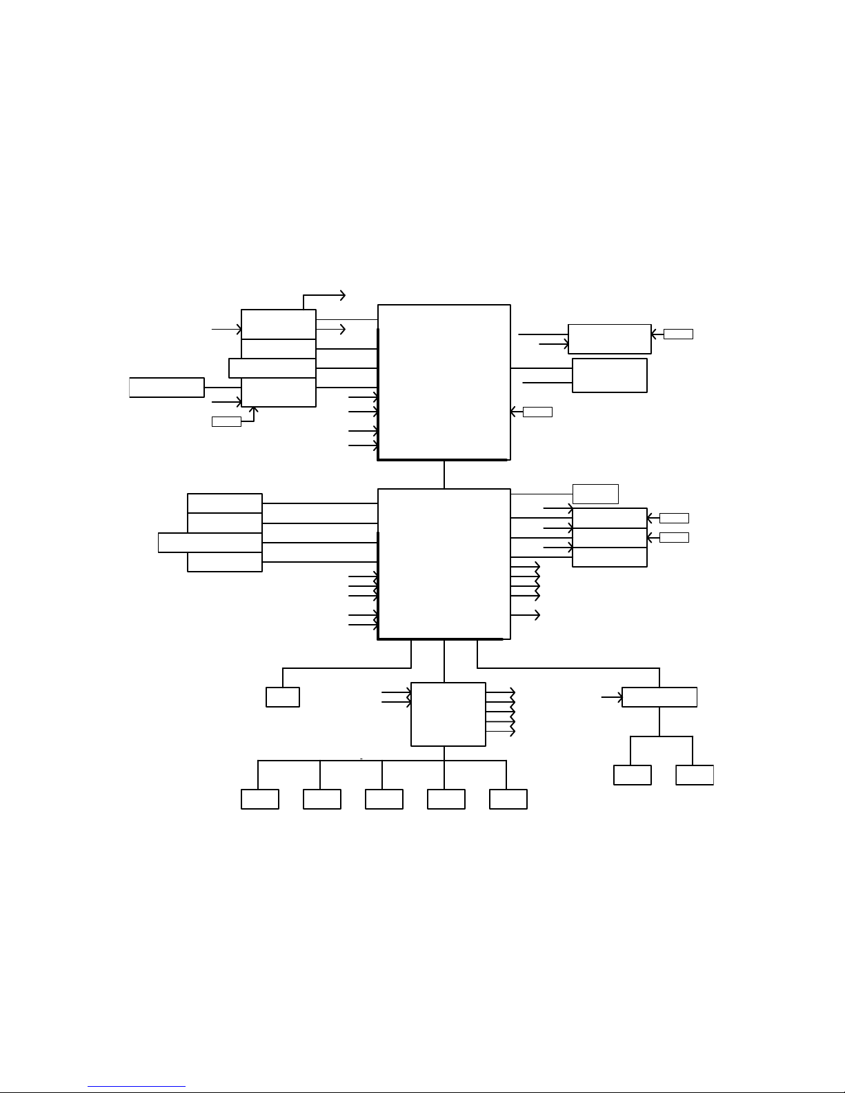
1.1 Block Diagram............................................................................................... 5
1.2 Features........................................................................................................ 6
1.3 PCB Layout ................................................................................................... 8
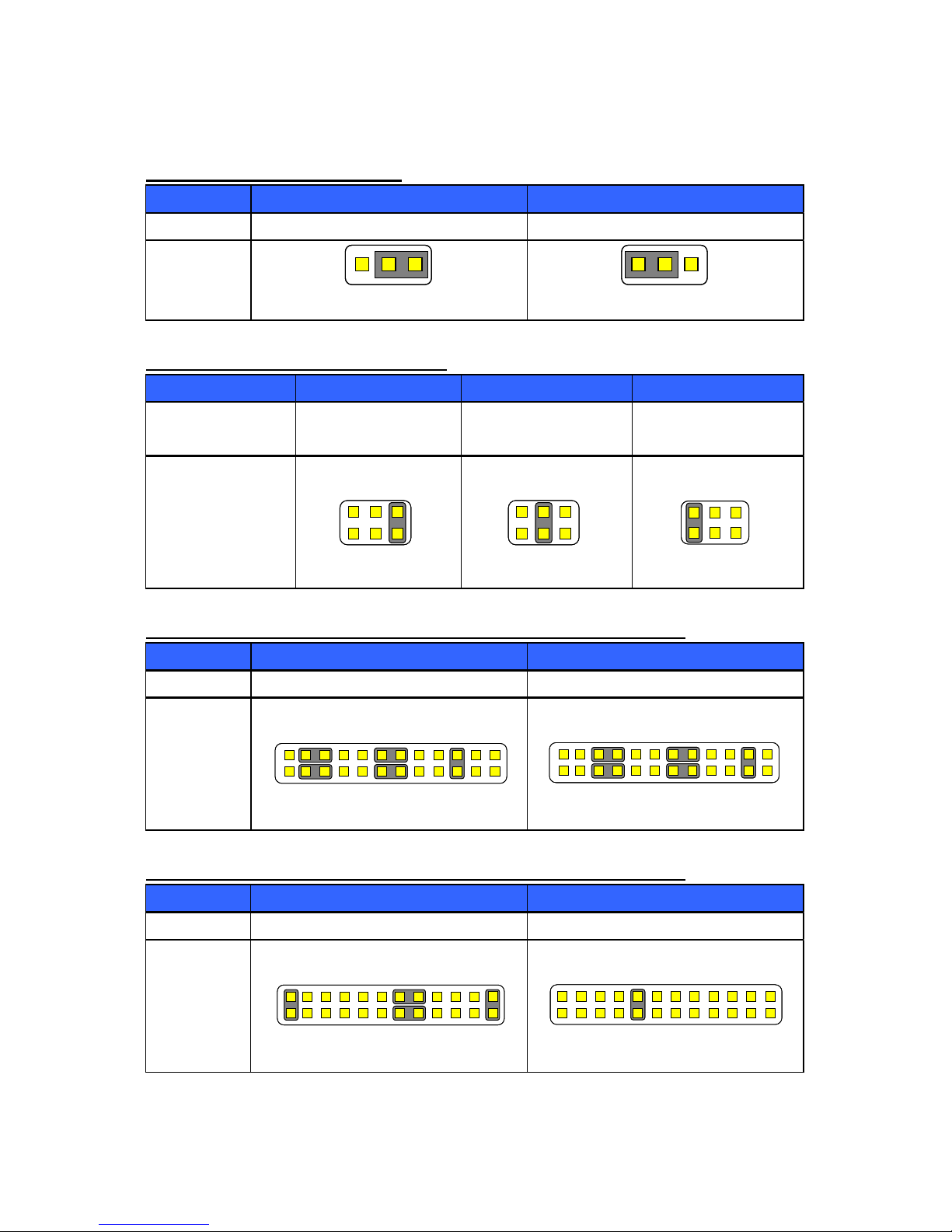
1.4 Jumper Setting .............................................................................................. 9
1.5 Connector Function List .............................................................................. 13
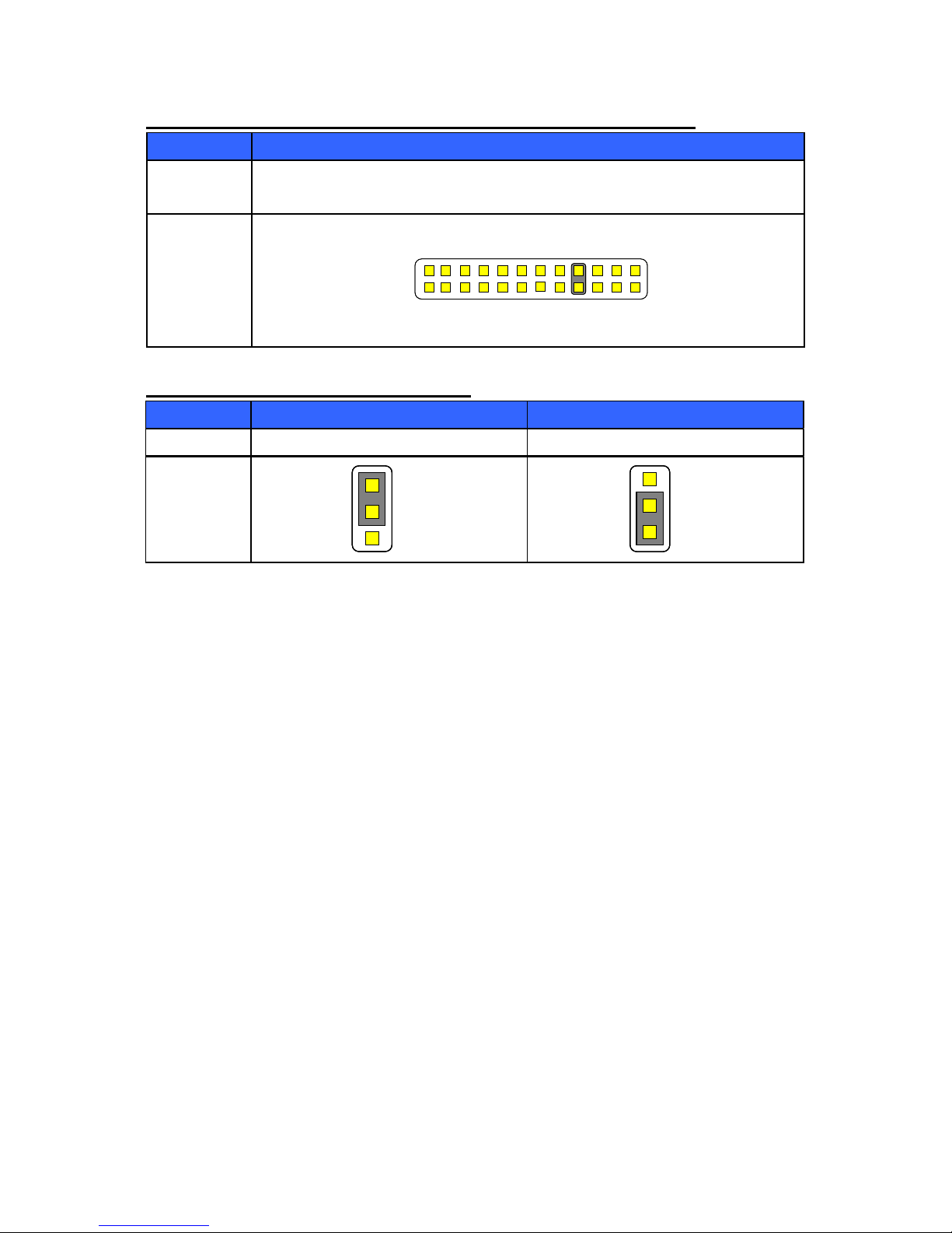
1.6 Internal Connector Pin Define ..................................................................... 14
Chapter 2 BIOS Setup.............................................................................................. 19
2.1 Main Menu .................................................................................................. 19
2.2 Advanced Menu .......................................................................................... 20
2.3 PCI Subsystem Setting ............................................................................... 21
2.4 Advanced BIOS Feature Setup ................................................................... 22
2.5 CPU Configuration ...................................................................................... 23
2.6 SATA Configuration ..................................................................................... 24
2.7 USB Configuration ...................................................................................... 25
2.8 Super IO Configuration ............................................................................... 27
2.9 Serial Port 0 Configuration .......................................................................... 28
2.10 Serial Port 1 Configuration ........................................................................ 29
2.11 Parallel Port Configuration......................................................................... 30
2.12 Pc Health Status........................................................................................ 31
2.13 Serial Super IO Configuration ................................................................... 32
2.14 Serial Port Configuration ........................................................................... 33
2.15 Chipset ...................................................................................................... 35
2.16 Memory Information .................................................................................. 36
2.17 Chipset Configuration................................................................................ 37
2.18 Intel IGD Configuration.............................................................................. 38
2.19 PCI Express Root Ports Configuration ...................................................... 40
2.20 USB Mode................................................................................................. 41
2.21 PCI Express Ports Configuration............................................................... 43
2.22 Boot Configuration .................................................................................... 45
2.23 Password Description ............................................................................... 47
2.24 Save Changes and Exit............................................................................. 48
Chapter 3 Drivers Installation ................................................................................... 49
3.1 Intel Chipset Device Software ..................................................................... 49
3.2 Intel Graphic Media Accelerator Driver........................................................ 52
3.3 LAN Driver................................................................................................... 55

K350-D25501 / K350-N26001 User Manual 4
3.4 Audio Driver................................................................................................. 57
Appendix-A Watchdog.............................................................................................. 58
Appendix-B GPIO..................................................................................................... 61

K350-D25501 / K350-N26001 User Manual 5
Chapter 1 Product Information
This chapter introduces the product features, jumper and connector information.
1.1 Block Diagram
RTC
32.768KHZ
WDTO_N
SIO_PWROK
PLTRST_N
SYS_PWRGD_TPT
25MHZ
25MHZ
27MHZ
H_PWRGD
RESET#
PWRGOOD
P 04
RSMRST#RSMRST#
H_PWRGDCPUPWRGD
PSIN PS_ON-
P 25
P 08
P 04,05,06.07
P 17
P 19
P 09,10,11
P 20
P 13
P 12
P 16 P 16
P 15P 15
P 21
P 18
SATA
V1.05_PWROK
PGOOD
DGRWP_XFGNO_RV
VCPU_PWROK
PGOODG
VRMPWRGDALL_SYS_PWRGD
P 17
P 17
P 18
P 18
SLP_S3_N
SLP_S4_N
SLP_S5_N
PM_PWRBTN_N
PM_PWRBTN_N
SLP_S3#
SYS_RESET#
PW RBTN#
FP_RST_N
SLP_S5#
SLP_S4#
27MHZ
PLTRST_R_N
PCIRST#
PLTRST#
P 23
P 22
P 24
P 29
DP
DP Signal CONN to DVI-D
ALL_SYS_PWRGD
PLTRST-
P 03
9VRS4339BKLF/MLF56
25MHZ
PLTRST- PLTRST-
LPC I/F
DDR3 800/1066MHz
DMI 4 Lanes
Intel
PLTRST-
COM2KB&MS
SM Bus
SM Bus
SO-DIMM
Intel ATOM
NM10
CG82NM10
PLTRST-
USB 2.0 x2
SIO_W83627EHG
SPI
LPT
PLTRST-
COM4COM3
COM1
SATA2 CONN or CFAST Socket
SATA1 CONN
DIO
VGA
SIO_ F81216D
SPI
PCIe x1
mini-PCIe Slot
PCIe x1
PCIe x1
LAN1_RTL8111E
HD Audio
CODEC_ALC662
D2 Series / N2 Series
eDP
LVDS 18/24bit CH7511
LAN2_RTL8111E
ISL95837HRZ
USB 2.0
SATA
SIO_RSMRST_N
P 25
SYS_PWRGD_TPT
DDR3_PWROK
DDR3_VCCA_PW ROK
DDR3_DRAM_PWROK
PWROK

K350-D25501 / K350-N26001 User Manual 6
1.2 Features
SystemProcessor/
Chipsets
Processor Intel ATOM Processor D2550 processor
on board
Chipset Intel D2550 + NM10
BIOS AMI
Memory Technology One 204-pin DDR3 1066 SO-DIMM
SDRAM, upgradable to 4GB
Display
Chipset Intel D2550 integrated
VRAM Share with System memory
Resolution Analog Display: Up to 2048 x 1536
(QXGA)
LVDS 24bit, Dual channel
LVDS Resolution Digital LVDS: Up to 1920 x 1200
Dual Display CRT+LVDS, CRT+DP, LVDS+DP
Ethernet Interface Dual 10/100/1000 Mbps
Controller Realtek 8111E GbE
Audio Interface High Definition Audio
Controller Realtek ALC662 HD CODEC
SATA
Max. Data
Transfer
300 MB/s
Port 1
Expansion Bus Mini-PCIe 1
Onboard
Pin-Header
LVDS 1
USB 2.0 2
COM 3
Parallel 1
DP 1
Audio Header 1 (Mic.-In, Line-in, Line-out)
C-Fast 1
DIO *Note1 8-bit Digital I/O (4 In + 4 Out)
PS/2 1 (K/B and Mouse)
Rear I/O
COM 1 x (RS232/422/485), support 5V & 12V by
jumper selector
VGA 1
LAN 2 x RJ45
USB 2.0 2

K350-D25501 / K350-N26001 User Manual 7
Power Connector Type 4-pin DC-in power connector
Mode AT/ATX Mode support (by jumper selector)
Watchdog Timer Interval Programmable 1~255 sec./min.
Output System reset
Environment
*Note2
Operating Temp. 0°C~ 60°C
Storage Temp. -20°C~ 80°C
Relative
Humidity
0%~ 95% (non-condensing)
Form Factor Dimension (L*W) 146mm x 102mm
*Note:
1. Digital I/O:
Input: 12V-tolerance & TTL inputs with ESD protection.
Output: Open-drain outputs with minimum100mA sinking capability.
2. Laboratory Stress Test Results:
Operating Temperature: 0°C ~ 60°C (0%~95% R.H., non-condensing)
Cold Boot Temperature: -40°C

K350-D25501 / K350-N26001 User Manual 8
1.3 PCB Layout
KB_MS1
JFRONT
H2 JLVDS1 LCD1 JLVDS_SEL1 DB1 JCMOS BAT1
PWR1
H4
AUDIO1
U12
JSPI1
USB2
SATA_PWR1
H3
SATA1
USB1
LAN2LAN1
JCOM2
COM2
JCOM2_SEL1
VGA1
COM4COM3
H1
J
PWR_SEL1
CPUFAN1
LPT1
LPC1
DIO1
MINI-PCIE1
U7
INV1
COM1

K350-D25501 / K350-N26001 User Manual 9
1.4 Jumper Setting
JCMOS: CMOS Clear (2.54mm)
Pin No. 1-2 2-3
Function Normal Operation (Default) Clear CMOS Contents
Jumper
Setting
3 2 13 2 1
3 2 13 2 1
JCOM2: (5V/12V/RI) Select (2.54mm)
Pin No. 1-2 3-4 5-6
Function +5V Modem Ring In
(Default)
+12V
Jumper Setting
JCOM2_SEL: COM2 (RS-232/RS-422/RS-485) Select (1/3) (2.0mm)
Pin No. 5-6, 11-13, 12-14, 19-21, 20-22 3-4, 9-11, 10-12, 17-19, 18-20
224-SR)tluafeD(232-SRnoitcnuF
Jumper
Setting
JCOM2_SEL: COM2 (RS-232/RS-422/RS-485) Select (2/3) (2.0mm)
Pin No. 1-2, 9-11, 10-12, 23-24 15-16
Function RS-485 RS-422 RX 100 Termination
Jumper
Setting
23 1
24 2
23 1
24 2
23 1
24 2
23 1
24 2
23 1
24 2
23 1
24 2
23 1
24 2
23 1
24 2
6 4 2
5 3 1
6 4 2
5 3 1
6 4 2
5 3 1
6 4 2
5 3 1
6 4 2
5 3 1
6 4 2
5 3 1

K350-D25501 / K350-N26001 User Manual 10
JCOM2_SEL1: COM2 (RS-232/RS-422/RS-485) Select (3/3) (2.0mm)
Pin No. 7-8
Function RS-422 TXD Pair 100 (Not recommended)/
RS-485 Data Pair Termination
Jumper
Setting
JLVDS1: LCD Power (+3.3V/+5V) Select
Pin No. 1-2 2-3
Function LCD Power +3.3V (Default) LCD Power +5V
Jumper
Setting
1
2
3
1
2
3
1
2
3
1
2
3
23 1
24 2
23 1
24 2

K350-D25501 / K350-N26001 User Manual 11
JLVDS_SEL1: LVDS Panel Type Select
Pin No. Jumper Setting LVDS Panel Type
1-2, 3-4, 5-6, 7-8
(Default)
800*600/18bit
Single Channel
3-4, 5-6, 7-8
1024*768/18bit
Single Channel
1-2, 5-6, 7-8
1024*768/24bit
Single Channel
5-6, 7-8
1 3 5 7
2 4 6 8
1280*768/18bit
Single Channel
1-2, 3-4, 7-8
1 3 5 7
2 4 6 8
1280*800/18bit
Single Channel
3-4, 7-8
1280*960/18bit
Single Channel
1-2, 7-8
1280*1024/24bit
Dual Channel
7-8
1366*768/18bit
Single Channel
1-2, 3-4, 5-6
1366*768/24bit
Single Channel
1 3 5 7
2 4 6 8
1 3 5 7
2 4 6 8
1 3 5 7
2 4 6 8
1 3 5 7
2 4 6 8
1 3 5 7
2 4 6 8
1 3 5 7
2 4 6 8
1 3 5 7
2 4 6 8

K350-D25501 / K350-N26001 User Manual 12
3-4, 5-6
1400*900/24bit
Dual Channel
1-2, 5-6
1 3 5 7
2 4 6 8
1400*1050/24bit
Dual Channel
5-6
1 3 5 7
2 4 6 8
1600*900/24bit
Dual Channel
1-2, 3-4
1 3 5 7
2 4 6 8
1680*1050/24bit
Dual Channel
3-4
1 3 5 7
2 4 6 8
1600*1200/24bit
Dual Channel
1-2
1 3 5 7
2 4 6 8
1920*1080/24bit
Dual Channel
NC
1 3 5 7
2 4 6 8
1920*1200/24bit
Dual Channel
JPWR_SEL1: AT/ATX Mode Select
Pin No. 1-2 2-3
)tluafeD(edoMXTAedoMTAnoitcnuF
Jumper
Setting
1
2
3
1
2
3
1
2
3
1
2
3
1 3 5 7
2 4 6 8

K350-D25501 / K350-N26001 User Manual 13
1.5 Connector Function List
Connector Function Note
AUDIO1 Audio Amplifier Output with Wafer connector
COM1, 3, 4 Serial Port with Box-header
COM2 Serial Port with DSUB-9P connector
CPUFAN1 CPUFAN 3-pin connector
DIO1 Digital I/O with Pin-header
INV1 Inverter with Box-header
JFRONT Front Panel with Pin-header
KB_MS1 Keyboard and mouse connector
rotcennocNAL2,1NAL
LCD1 LVDS Panel Signal with Box-header
LPC1 Debug Port with Pin-header
LPT1 Parallel Port with Box-header
MINI-PCIE1 Mini PCI Express connector
rotcennoc2x2XTA1RWP
rotcennocATAS1ATAS
SATA_PWR1, SATA Power with Box-header
USB1 USB0/1 Port connector
USB2 USB2/3 connector with Pin-header
rotcennocAGV1AGV

K350-D25501 / K350-N26001 User Manual 14
1.6 Internal Connector Pin Define
1
2
10
9
AUDIO: Audio Amplifier Output with Wafer connector (2.0mm)
Pin No. Signal Pin No. Signal
1 Line-In Right 2 Line-In Left
3 Line-In Jack Detect 4 MIC Jack Detect
5 MIC-In Right 6 MIC-In Left
7 Line-Out Jack Detect 8 Audio Ground
9 Line-Out Right 10 Line-Out Left
1
2
10
9
COM1, 3, 4: Serial Port with Box-header (2.0mm)
Pin No. Signal Pin No. Signal
1 DCD 2 DSR
3 RXD 4 RTS
5 TXD 6 CTS
7 DTR 8,10 RI/+5V/+12V
9 Ground
156273849
COM2: RS 232 Serial Port with DSUB-9P connector (1/3)
Pin No. Signal Pin No. Signal
1 DCD 2 RXD
3 TXD 4 DTR
5 Ground 6 DSR
7 RTS 8 CTS
9 RI/+5V/+12V
156273849
COM2: RS 422 Serial Port with DSUB-9P connector (2/3)
Pin No. Signal Pin No. Signal
1 DATA TX- 2 DATA TX+
3 DATA RX+ 4 DATA RX-
5 NC 6 NC
7 NC 8 NC
9 NC

K350-D25501 / K350-N26001 User Manual 15
156273849
COM2: RS 485 Serial Port with DSUB-9P connector (3/3)
Pin No. Signal Pin No. Signal
1 DATA- 2 DATA+
3 NC 4 NC
5 NC 6 NC
7 NC 8 NC
9 NC
1
3
CPUFAN: 3Pin FAN connector
Pin No. Signal
1 Ground
2 Fan Power (+12V)
3 Speed Sense
12
10
11
DIO: Digital I/O with Pin-header (2.00mm)
Pin No. Signal Pin No. Signal
1 DIO-Out0 2 DIO-In0
3 DIO-Out1 4 DIO-In1
5 DIO-Out2 6 DIO-In2
7 DIO-Out3 8 DIO-In3
9 +12V 10 +5V
11 Ground
15
INV1: Inverter with Box-header (2.50mm)
Pin No. Signal
1 +12V
2 +12V
3 Ground
4 Inverter Brightness control
5 Inverter Enable

K350-D25501 / K350-N26001 User Manual 16
12
9
10
JFRONT: Front Panel Connector with Pin-header (2.54mm)
Pin No. Signal Pin No. Signal
1 Power LED +
(+5V, 470)
2 Power LED – (Ground)
3 HDD LED + (470) 4 HDD LED -
5 Suspend LED +
(+V5S, 470)
6 Suspend LED -
7 Reset Switch + 8 Reset Switch –
(Ground)
9 Power Switch + 10 Power Switch –
(Ground)
1
6
KB_MS1: Keyboard and mouse connector (2.00mm)
Pin No. Sgnal
1 PS2 Power (+5V)
2 PS2 Mouse Data
3 PS2 Mouse Clock
4 PS2 Keyboard Data
5 PS2 Keyboard Clock
6 PS2 Ground
1
2
2
9
30
LCD1: LVDS Panel Signal with Box-header (1.0mm)
Pin No. Signal Pin No. Signal
1 Ground 2 Ground
3 LA_DC3+ 4 LA_DC3-
5 LA_CLK+ 6 LA_CLK-
7 LA_DC2+ 8 LA_DC2-
9 LA_DC1+ 10 LA_DC1-
11 LA_DC0+ 12 LA_DC0-
13 Ground 14 Ground
15 LB_DC7P 16 LB_DC7N
17 LB_CLK2P 18 LB_CLK2N
19 LB_DC6P 20 LB_DC6N
21 LB_DC5P 22 BL_DC5N
23 LB_DC4P 24 LB_DC4N

K350-D25501 / K350-N26001 User Manual 17
25 Ground 26 Ground
27 LVDS Power 28 LVDS Power
29 LVDS Power 30 LVDS Power
Note1: LVDS Power = +5V or +3.3V (Default)
21
9
8
LPC1: Debug Port with Pin-header (2.0mm)
Pin No. Signal Pin No. Signal
1 LAD0 2 LPC Reset#
3 LAD1 4 LFRAME#
5 LAD2 6 +3.3V
7 LAD3 8 Ground
9 LPC33MHz 10 NC
1
14
13
26
LPT1: Parallel Port with Box-header (2.0mm)
Pin No. Signal Pin No. Signal
1 Strobe# 14 Auto Form Feed#
2 Data 0 15 Error#
3 Data 1 16 Initialization#
4 Data 2 17 Printer Select IN#
5 Data 3 18 Ground
6 Data 4 19 Ground
7 Data 5 20 Ground
8 Data 6 21 Ground
9 Data 7 22 Ground
10 Acknowledge# 23 Ground
11 Busy 24 Ground
12 Paper Empty 25 Ground
13 Printer Select 26 Ground
21
34
PWR1: ATX 2x2 +9V ~ +36V Input (4.20mm)
Pin No. Signal Pin No. Signal
1 Ground 2 Ground
3 +9V ~ +36V
4 +9V ~ +36V

K350-D25501 / K350-N26001 User Manual 18
1
7
SATA1: SATA Connector (2.50mm)
Pin No. Signal
1 Ground
2 TX+
3 TX-
4 Ground 1
5 RX-
6 RX+
7 Ground 2
1
4
SATA_PWR1: SATA Power with Box-header (2.50mm)
Pin No. Signal
1 +5V
2 Ground
3 Ground
4 +12V
17
2
8
USB2/3: USB connector with Pin header (2.0mm)
Pin No. Signal Pin No. Signal
1 USB Power (+5V) 2 USB Power (+5V)
3 USB DATA- 4 USB DATA-
5 USB DATA+ 6 USB DATA+
7 Ground 8 Ground

K350-D25501 / K350-N26001 User Manual 19
Chapter 2 BIOS Setup
This chapter introduces BIOS setup information.
Power on or reboot the system board, when screen appears message as “Press DEL
to enter SETUP.” Press <DEL> to run BIOS SETUP Utility.
Note: The BIOS configuration for reference only, it may subject to change without
prior notice.
2.1 Main Menu
$SWLR 6HWXS8WLOLW\ &RS\ULJKW&$PHULFDQ0HJDWUHQGV,QF
0DLQ$GYDQFHG&KLSVHW%RRW6HFXULW\6DYH([LW
&KRRVHWKHV\VWHP
GHIDXOWODQJXDJH
(QWHU6HOHFW
&KDQJH2SW
)*HQHUDO+HOS
)3UHYLRXV9DOXHV
)2SWLPL]HG'HIDXOWV
)6DYH([LW
(6&([LW
Main
6HOHFW6FUHHQ
6HOHFW,WHP
Version 2.14.1219. Copyright (C) 2011 American Megatrends, INC.
%,26 ,QIRUPDWLRQ
%,269HQGRU
&RUH9HUVLRQ
&RPSOLDQF\
3URMHFW9HUVLRQ
0RGHO1DPH
%,269HUVLRQ
%XLOG'DWHDQG
7LPH
6\VWHP/DQJXDJH
6\VWHP'DWH
6\VWHP7LPH
$FFHVV/HYH
$PHULFDQ0HJDWUHQGV
8(),3,
$3-.
:(&;'
5$
>(QJOLVK@
>0RQ@
>@
$GPLQLVWUDWRU
ϭDate
Set system date.
ϭTime
Set system time.

K350-D25501 / K350-N26001 User Manual 20
2.2 Advanced Menu
This section allows you to configure CPU and other system devices for basic operation
through the following sub-menus.
$SWLR 6HWXS8WLOLW\ &RS\ULJKW&$PHULFDQ0HJDWUHQGV,QF
0DLQ$GYDQFHG&KLSVHW%RRW6HFXULW\6DYH([LW
%RRW2SWLRQIRUUHO7HN
(1,&
(QWHU6HOHFW
&KDQJH2SW
)*HQHUDO+HOS
)3UHYLRXV9DOXHV
)2SWLPL]HG'HIDXOWV
)6DYH([LW
(6&([LW
Advanced
6HOHFW6FUHHQ
6HOHFW,WHP
/HJDF\2S5206XSSRUW
2QERDUG3;(2S520
:DNH2Q3&,H/DQ
:DNH2Q5LQJ
/DXQFK6WRUDJH2S520
3&,
$&3,
&38
,'(
86%
6XSHU
+:
6HFRQG
WATX-Q670 BIOS RA01 20120104Version 2.14.1219. Copyright (C) 2011 American Megatrends, INC.
6XEV\VWHP6HWWLQJV
6HWWLQJV
&RQILJXUDWLRQ
&RQILJXUDWLRQ
&RQILJXUDWLRQ
,2&RQILJXUDWLRQ
0RQLWRU
,2&RQILJXUDWLRQ
>'LVDEOHG@
>'LVDEOHG@
>'LVDEOHG@
>(QDEOHG@
ϭOnboard PXE OpROM
Choices: Disabled, Enabled.
ϭWake On PCIe Lan
Choices: Disabled, Enabled.
ϭWake On Ring
Choices: Disabled, Enabled.
ϭLaunch Storage OpROM
Enabled: Use this setting to specify that legacy PCI option ROMs for PCI storage
devices are to be loaded and executed.
This manual suits for next models
1
Table of contents