LG LAC6700R User manual

CAR CD/MP3/WMA
RECEIVER
SERVICE MANUAL
MODEL :
LAC6700R
CAUTION
BEFORE SERVICING THE UNIT, READ THE “SAFETY PRECAUTIONS”
IN THIS MANUAL
.
MODEL: LAC6700R
SERVICE MANUAL
P/NO : AFN35097871
OCTOBER, 2007
Website http://biz.lgservice.com
Internal Use Only

1-1
CONTENTS
SECTION 1 SUMMARY
SERVICING PRECAUTIONS..........................................................................................................................................1-2
ESD PRECAUTIONS .......................................................................................................................................................1-3
SPECIFICATIONS.............................................................................................................................................................1-4
SECTION 2 ELECTRICAL
ELECTRICAL TROUBLESHOOTING GUIDE & WAVEFORMS .............................................................................2-1
1. MAIN, FRONT & TUNER PART................................................................................................................................2-1
2. CD PART TROUBLESHOOTING .............................................................................................................................2-4
3. USB PART TROUBLESHOOTING...........................................................................................................................2-7
• WAVEFORMS..............................................................................................................................................................2-9
INTERNAL BLOCK DIAGRAM OF ICs......................................................................................................................2-12
1. IC518, IC701 & IC702 (S4580) ...............................................................................................................................2-12
2. IC301 (HA13173AH) ................................................................................................................................................2-12
3. IC302 (BA00CCOWFP) ...........................................................................................................................................2-14
4. IC401 (µPD78F1164) ...............................................................................................................................................2-14
5. IC601 (TDA7419) .....................................................................................................................................................2-17
6. IC602 (NJM2706-DMP24) .......................................................................................................................................2-19
7. IC801 (TB2904HQ) ..................................................................................................................................................2-20
8. IC901 (LD3811) ........................................................................................................................................................2-21
BLOCK DIAGRAM .........................................................................................................................................................2-23
CIRCUIT DIAGRAMS.....................................................................................................................................................2-25
1. MAIN CIRCUIT DIAGRAM ......................................................................................................................................2-25
2. CDP 1 CIRCUIT DIAGRAM ....................................................................................................................................2-27
3. CDP 2 CIRCUIT DIAGRAM ....................................................................................................................................2-29
4. FRONT CIRCUIT DIAGRAM ..................................................................................................................................2-31
5. USB CIRCUIT DIAGRAM........................................................................................................................................2-33
6. LCD LIGHTING CIRCUIT DIAGRAM.....................................................................................................................2-34
PRINTED CIRCUIT DIAGRAMS..................................................................................................................................2-35
1. MAIN P.C.BOARD....................................................................................................................................................2-35
2. CDP P.C.BOARD .....................................................................................................................................................2-39
3. FRONT P.C.BOARD ................................................................................................................................................2-40
4. USB P.C.BOARD......................................................................................................................................................2-41
5. LCD LIGHTING P.C.BOARD...................................................................................................................................2-41
SECTION 3 EXPLODED VIEWS
1. CABINET AND MAIN FRAME SECTION ................................................................................................................3-1
2. MECHANISM(PICK-UP) SECTION..........................................................................................................................3-3
SECTION 4 REPLACEMENT PARTS LIST.............................................................4-1
Copyright © 2007 LG Electronics. Inc. All right reserved.
Only for training and service purposes
LGE Internal Use Only

1-2
1. Always disconnect the power source before:
1) Removing or reinstalling any component, circuit board, module or any other instrument assembly.
2) Disconnecting or reconnecting any instrument electrical plug or other electrical connection.
3) Connecting a test substitute in parallel with an electrolytic capacitor in the instrument.
CAUTION: A wrong part substitution or incorrect polarity installation of electrolytic capacitors may result in an
explosion hazard.
2. Do not defeat any plug/socket B+ voltage interlocks with which instruments covered by this service
manual might be equipped.
3. Do not apply power to this instrument and or any of its electrical assemblies unless all solid-state
device heat sinks are correctly installed.
4. Always connect a test instrument’s ground lead to the instrument chassis ground before connecting
the test instrument positive lead. Always remove the test instrument ground lead last.
1) The service precautions are indicated or printed on the cabinet, chassis or components. When servicing,
follow the printed or indicated service precautions and service materials.
2) The Components used in the unit have a specified conflammability and dielectric strength. When replacing
any components, use components which have the same ratings. Components marked in the circuit diagram
are important for safety or for the characteristics of the unit. Always replace with the exact components.
3) An insulation tube or tape is sometimes used and some components are raised above the printed writing
board for safety. The internal wiring is sometimes clamped to prevent contact with heating components.
Install them as they were.
4) After servicing always check that the removed screws, components and wiring have been installed correctly
and that the portion around the service part has not been damaged. Further check the insulation between
the blades of attachment plug and accessible conductive parts.
SERVICING PRECAUTIONS
SECTION 1 SUMMARY
Copyright © 2007 LG Electronics. Inc. All right reserved.
Only for training and service purposes
LGE Internal Use Only

1-3
ESD PRECAUTIONS
Electrostatically Sensitive Devices (ESD)
Some semiconductor (solid state) devices can be damaged easily by static electricity. Such components
commonly are called electrostatically sensitive devices (ESD). Examples of typical ESD devices are
integrated circuits and some field-effect transistors and semiconductor chip components. The following
techniques should be used to help reduce the incidence of component damage caused by static electricity.
1. Immediately before handling any semiconductor component or semiconductor-equipped assembly, drain
off any electrostatic charge on your body by touching a know earth ground. Alternatively, obtain and
wear a commercially available discharging wrist strap device, which should be removed for potential
shock reasons prior to applying power to the unit under test.
2. After removing an electrical assembly equipped with ESD devices, place the assembly on a conductive
surface such as aluminum foil, to prevent electrostatic charge buildup or exposure of the assembly.
3. Use only a grounded-tip soldering iron to solder or unsolder ESD devices.
4. Use only an anti-static solder removal device. Some solder removal devices not classified as "anti-static"
can generate electrical charges sufficient to damage ESD devices.
5. Do not use freon-propelled chemicals These can generate electrical charges sufficient to damage ESD
devices.
6. Do not remove a replacement ESD device from its protective package until immediately before you are
ready to install it. (Most replacement ESD devices are packaged with leads electrically shorted together
by conductive foam, aluminum foil or comparable conductive materials).
7. Immediately before removing the protective material from the leads of a replacement ESD device, touch
the protective material to the chassis or circuit assembly into which the device will by installed.
CAUTION : BE SURE NO POWER IS APPLIED TO THE CHASSIS OR CIRCUIT, AND OBSERVE ALL
OTHER SAFETY PRECAUTIONS.
8. Minimize bodily motions when handing unpackaged replacement ESD devices. (Otherwise harmless
motion such as the brushing together of your clothes fabric or the lifting of your foot from a carpeted floor
can generate static electricity sufficient to damage an ESD device).
CAUTION. GRAPHIC SYMBOLS
THE LIGHTNING FLASH WITH ARROWHEAD SYMBOL. WITHIN AN EQUILATERAL
TRIANGLE, IS INTENDED TO ALERT THE SERVICE PERSONNEL TO THE PRESENCE
OF UNINSULATED "DANGEROUS VOLTAGE" THAT MAY BE OF SUFFICIENT
MAGNITUDE TO CONSTITUTE A RISK OF ELECTRIC SHOCK.
THE EXCLAMATION POINT WITHIN AN EQUILATERAL TRIANGLE IS INTENED TO
ALERT THE SERVICE PERSONNEL TO THE PRESENCE OF IMPORTANT SAFETY
INFORMATION IN SERVICE LITERATURE.
Copyright © 2007 LG Electronics. Inc. All right reserved.
Only for training and service purposes
LGE Internal Use Only

1-4
SPECIFICATIONS
• GENERAL
Output Power 50W x 4CH (Max.)
Power Source DC 12V
Speaker impedance 4Ω
Ground System Negative
Dimensions (W x H x D) 180 x 51 x 171mm (Without Control Panel)
Net Weight 2.0kg
• CD SECTION
Frequency Response 20Hz ~ 20kHz
S/N Ratio 85dB
Distortion 0.05%
Channel Separation (1kHz) 60dB
• RADIO SECTION
FM
Frequency Range 65 ~ 74, 87.5 ~ 107.9 or 87.5 ~ 108MHz
S/N Ratio 53dB
Distortion 0.7%
Usable Sensitivity 12dBµV
AM (MW)
Frequency Range 520 ~ 1720 or 522 ~ 1620kHz
S/N Ratio 45dB
Distortion 1.0%
Usable Sensitivity 28dBµV
• USB SECTION
Version USB 1.1
Copyright © 2007 LG Electronics. Inc. All right reserved.
Only for training and service purposes
LGE Internal Use Only

2-1
SECTION 2 ELECTRICAL
1. MAIN, FRONT & TUNER PART
No Symptom Check Point Location No.
SYSTEM CONTROL
1No Power Checked the Fuse. CN801
Checked the Back up Vdd, Gnd. CN801(16, 15)
Checked the Micom Back Up Vdd. IC301(14),D307, IC401(30,47,50,99,100)
Checked the Micom Ground. IC401(20,51,97,98)
Checked the Reset. IC402. IC401(90)
Checked the X-tal. X401, X402
Checked the ACC in. Q301,Q302, IC401(38), CN801(14)
Checked the detachable switch. SW401, IC401(73)
Checked the flipdown Detector. CN901(19), IC401(74)
Checked the Key line. IC401(52,53)
2Not available Remocon Checked the Remocon Sens Vdd. CN901(14),Q316,Q317,D307
Checked the Remocon Sens line. RM901, IC401(5)
3Not available to Volume control Checked the Encoder Volume. SW901, IC401(40,41)
4Not available to Key Control Checked Tact switch. SW902 ~ SW918
Checked Key line. IC410(52,53)
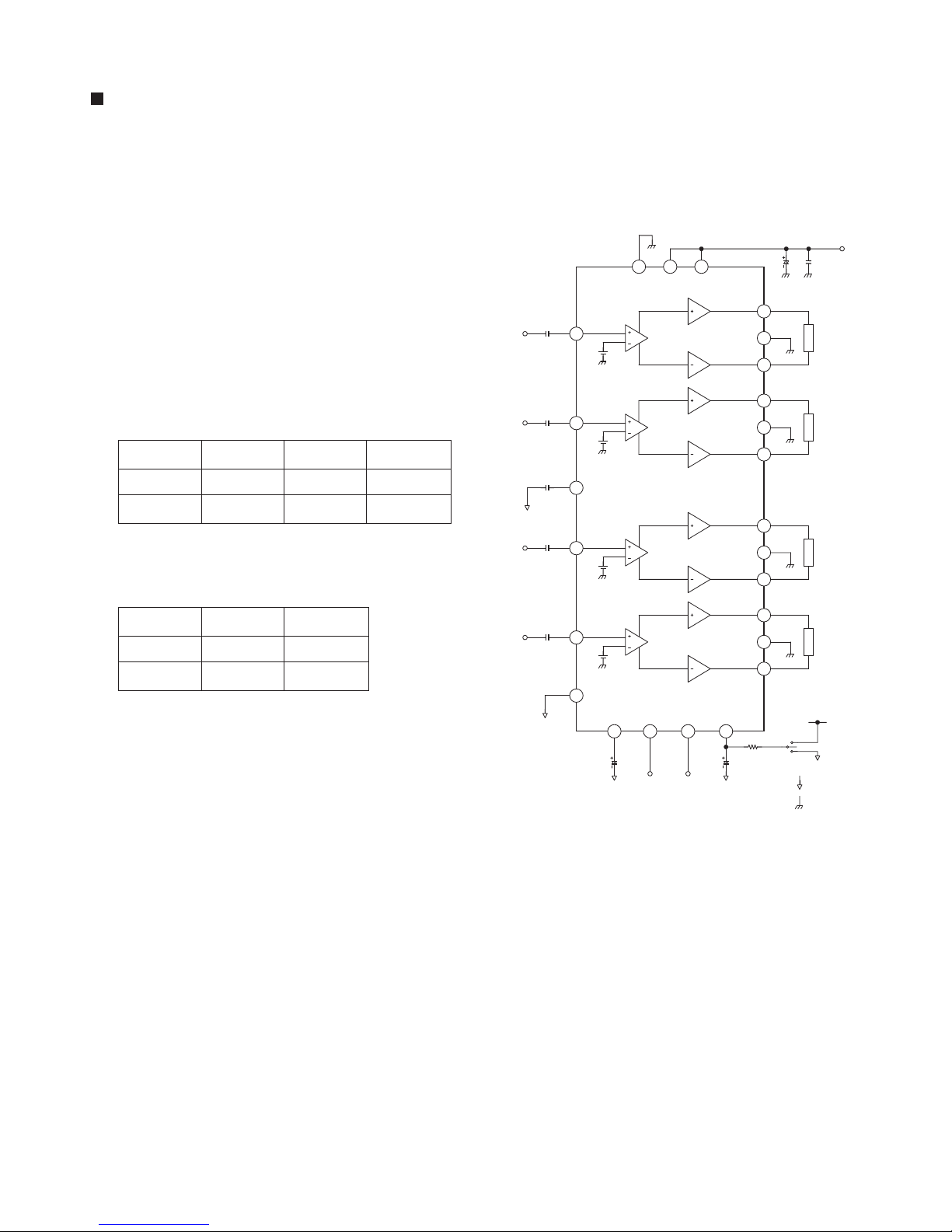
5No sound Checked the E-VR Vdd. IC301(10),IC601(24)
Checked the E-VR Ground. IC601(15)
Checked the E-VR control. IC601(22,23), IC401(1,2)
Checked the E-VR Signal in/out. IC601(5,6,7,8,9,10,11,13)
IC601(17,18,19,20)
Checked the E-VR Mute Control IC601(21), IC401(6)
* Power IC Checked the Power IC Vdd. IC801(6, 20)
: Refer to next page Checked the Power IC Ground. IC801(1, 2, 8, 13, 18, 24)
Checked the Power IC Control. IC801(4, 22), IC401(3,10)
Checked the Power IC Signal in/out. IC801(11,12, 14, 15)
IC801(3,5,7,9,17,19,21,23)
Checked the Power IC Mute. IC801(22)
Checked the Power IC Standby. IC801(4)
Checked the Power IC Ripple. IC801(10)
Checked the Main Connector.CN801(1,2, 3, 4, 8, 9, 12, 13)
6No Line out signal Checked the E-VR Vdd. IC301(10),IC601(24)
Checked the E-VR Ground. IC601(15)
Checked the E-VR control. IC601(22,23), IC401(1,2)
Checked the E-VR Signal in/out. IC601(5,6,7,8,9,10,11,13)
IC601(17,18,19,20)
Checked the OPAMP Vdd. IC701(8),IC702(8)
Checked the OPAMP Ground. IC701(4),IC702(4)
Checked the OPAMP Signal in/out IC701(3,5,7,1)
IC702(3,5,7,1)
Checked the Line out Mute circuit Q705,IC401(48)
Check the Line out Jack CN703
8Heard Pop Noise Checked the Mute Control. IC601(21), IC801(4, 22), IC401(3,6,10)
Checked the AF Mute. TU101(19), IC401(4)
9Not avaliable to Telephone Mute Checked the telephone Mute Control. CN801(5), Q305,Q306, IC401(62)
Checked the Mute Control. IC601(21), IC801(4, 22), IC401(3,6,10)
10 Not avaliable to ANT(Motor Type) Control Checked the ANT Control. IC301(12,13),IC401(87)
11 Not avaliable to Remote Checked the Remote control. CN801(6), IC402(1,2,4),Q308,Q309
(External AMP) IC401(63,64)
12 No output Beep sound. Checked the Beep Control. IC401(80), BU301
ELECTRICAL TROUBLESHOOTING GUIDE & WAVEFORMS
Copyright © 2007 LG Electronics. Inc. All right reserved.
Only for training and service purposes
LGE Internal Use Only

2-2
CAUTION - Tip for repair
Before exchange power amp IC(TB2904) for no audio problem, you have to check
below list.
1. Check VCC (pin 20, 6) & GND
2. Check input pin 11, 12, 14, 15
3. Check Standby, pin 4
: Follow the below list.
4. Check Mute function, pin 22
: Follow the below list.
5. Check Ripple pin 10.
: Normally it is high (about 10V)
6. Re-soldering all the pin of IC.
: Prevent crack of solder line.
* Keep changed IC, We request that you send it to HQ.
RL
RL
RL
11
9
8
7
5
2
3
17
18
19
21
24
23
12
15
14
120 6
RL
IN1
IN2
IN3
IN4
13
C1
C1
C1
C1
PRE-GND
10 25 22
OUT1 +
+
+
+
-
-
-
-
()
PW-GND1
OUT1 ( )
OUT2 ( )
PW-GND2
OUT2 ( )
OUT3 ( )
PW-GND3
OUT3 ( )
OUT4 ( )
PW-GND4
OUT4 ( )
TAB VCC1 VCC2
C3
C4
C2
: PRE-GND
: PW-GND
STBYRIP MUTE
C5
16
C6
4
OFF-SET
DET
MUTE
PLAY
5 V
R1
A
C-GND
Stand-by Power Sound Voltage
ON OFF OFF 0 to 1.5
OFF ON ON 3.5 to 6V
Mute Sound Voltage
ON OFF 0 to 1.5
OFF ON 3.5 to 6V
Picture 1) Power IC desc.
Copyright © 2007 LG Electronics. Inc. All right reserved.
Only for training and service purposes
LGE Internal Use Only

2-3
No Symptom Check Point Location No.
DISPLAY & LIGHTING
1No Display or Checked the LCD DRV Vdd. Q322,Q316,Q317
Some Display is broken IC901(69,70,71,72,73)
Checked the LCD DRV Ground. IC901(74)
Checked the LCD DRV OSC. IC901(75,76)
Checked the LCD DRV control. IC401(75,79,85,86),
IC901(77,78,79,80)
Checked the LCD DRV to LCD Pattern.
IC901(1 ~ 68)
2No LCD Lighting or Checked the LCD Lighting VDD. Q319,Q320,Q322,IC301(4,9)
Color is different IC401(64)
Checked the LED. LD991, LD992
3Not avaliable to LCD Lighting Checked the LCD Lighting Control. CN801(11),Q303,Q304,Q321,
control IC401(58)
Checked the LED. LD991,LD992
4No Key Lighting Checked the LED Lighting Vdd. IC301(4,9),IC401(64)
Checked the LED. LD901 ~ LD921
5Don't moved Level bar Checked the Level Meter control. IC601(25,26),IC401(9,54)
6Not avaliable to Dimmer control Chekced the Dimmer control. CN801(11),Q303,Q304,IC301(4,9)
No Symptom Check Point Location No.
TUNER FUNCTION
1Not available to Tuner Checked the Tuner Vdd. TU101(4,16),IC301(10),IC401(39)
Q350,Q351
Checked the Tuner Ground. TU101(3, 5,10,17)
Checked the PLL data. TU101(11,12,13,14,15)
IC401(67,68,44,45,46)
Checked the RF signal in. TU101(1, 2)
Checked the S-Meter control. TU101(7)
Checked the SD & ST IND. TU101(6)
2 Tuner no sound Checked the Tuner Signal out. TU101(8,9), IC601(5,6)
Checked the AF mute. TU101(19), IC401(4)
3Not available to RDS Checked the RDS data. TU101(20,21), IC401(65,83)
Copyright © 2007 LG Electronics. Inc. All right reserved.
Only for training and service purposes
LGE Internal Use Only

2-4
Something wrong with the CD player?
No loading?
OK
YES
CN510(13, 6)
YES
NO
Checked the CD Vdd?
IC506(26, 32, 47, 78, 18)
YES
NO
Checked the CD DSP ground?
IC504(7, 8, 20)
YES
NO
Checked the motor DRV
VDD?
IC506(72)
YES
NO
Checked the CD DSP reset?
X503
YES
NO
Checked the CD DSP X-tal?
PN504(3)
YES
NO
Fig 3, 4
Fig 1, 2
Fig 1, 2
Checked the disc in
load switch?
CN510(12, 17)
IC513(12, 14, 15)
YES
NO
Checked the loading
motor control?
PN504(1)
YES
NO
Checked the 8/12cm
sens switch?
2. CD PART TROUBLESHOOTING
A B C
Copyright © 2007 LG Electronics. Inc. All right reserved.
Only for training and service purposes
LGE Internal Use Only

2-5
No reading & "FILE CHECK"
DISPLAY?
OK
YES
PN504(4)
YES
NO
Fig 1, 2
Fig 3, 4
Fig 10~12
Fig 5
Fig 5
Fig 9
Fig 9
Fig 7
Fig 13
Fig 6
Checked the limit switch?
CN510(16)
YES
NO
Checked the motor DRV
mute control?
D5, D6
YES
NO
Checked the motor
LD control?
IC506(67, 68, 69, 70, 71)
YES
NO
Checked the CD DSP control?
IC506(25)
IC513(17, 18)
YES
NO
Checked the focus control?
IC506(25)
R517
YES
NO
Checked the focus error
level out.(FE mon)?
IC506(54)
YES
NO
Checked the PLL locking.
(FSEQ)?
IC506(41, 16)
YES
NO
Checked the RF signal
out check?
IC506(21)
IC513(8, 5)
YES
NO
Checked the spindle
motor control?
PN504(5, 6)
YES
NO
Checked the TRVP control?
IC506(24)
IC513(19, 20)
YES
NO
Checked the tracking control?
A
Copyright © 2007 LG Electronics. Inc. All right reserved.
Only for training and service purposes
LGE Internal Use Only

2-6
CD no sound?
OK
YES
IC520(1, 2, 3)
YES
NO
Fig 8
Fig 3, 4
Checked the DAC signal in?
B
No ejected the CD?
OK
YES
CN901(16) [MAIN]
YES
NO
Checked the Eject key?
YES
D6, D5
NO
Checked the loading motor
control?
C
Copyright © 2007 LG Electronics. Inc. All right reserved.
Only for training and service purposes
LGE Internal Use Only

2-7
Something wrong with the USB?
Only "NO USB" or "USB CHECK" display?
OK
IC512(2), L507, L508, L509, R566
YES
NO
Checked the USB Vdd?
IC511(17, 37, 40, 61, 71)
YES
NO
Checked the USB
interface IC ground?
IC505(24)
YES
NO
Checked the memory
IC ground?
IC511(57), CN510(31)
YES
NO
Checked the USB
interface IC reset?
X505
YES
NO
Checked the USB
interface IC X-tal?
IC511(65)
YES
NO
Fig 14
Checked the Flash
memory option port?
IC511(62, 63)
YES
NO
Checked the D+/D- port?
IC511(27)
YES
NO
Checked the USB
indication port?
IC506 (62, 63, 64)
YES
NO
Checked the USB
interface IC control?
3. USB PART TROUBLESHOOTING
D
YES
Copyright © 2007 LG Electronics. Inc. All right reserved.
Only for training and service purposes
LGE Internal Use Only

2-8
"FILE CHECK" display?
OK
OK
IC506(26, 31, 57, 60, 79 )
YES
NO
Checked the CD DSP ground?
IC506(72)
YES
NO
Checked the CD DSP reset?
X503
YES
NO
Checked the CD DSP X-tal?
IC506(67, 68, 69, 70, 71, 72, 73)
YES
NO
Fig 10~12
Checked the CD DSP control?
IC511(22, 23) IC510(50, 51)
YES
NO
Checked the USB data?
D
YES
USB no sound?
IC520(1, 2, 3)
YES
NO
Fig 8
Checked the CD DSP
signal out?
YES
YES
Copyright © 2007 LG Electronics. Inc. All right reserved.
Only for training and service purposes
LGE Internal Use Only

2-9
• WAVEFORMS
Fig 1) Switching condition for loading
PN504:[PIN3]
PN504:[PIN1]
PN504:[PIN4]
LOADING
12/8 S/W
LIMIT S/W
Fig 2) Switching condition for unloading
PN504:[PIN3]
PN504:[PIN1]
PN504:[PIN4]
LOADING
12/8 S/W
LIMIT S/W
Fig 3) Motor control signal for loading
REW
FEW
SLED CON
LOADING IN
PIN504:[PIN5]
PIN504:[PIN6]
R5091:[SLED CON]
R5465:[LOAD IN]
SL-
SL+
SLED CON
LOADING IN
Fig 4) Motor control signal for unloading
REW
FEW
SLED CON
LOADING IN
PIN504:[PIN5]
PIN504:[PIN6]
R5091:[SLED CON]
R5465:[LOAD IN]
SL-
SL+
SLED CON
LOADING IN
D6:[REW]
D5:[FEW]
R5091:[SLED CON]
R5465:[LOAD IN]
D6:[REW]
D5:[FEW]
R5091:[SLED CON]
R5465:[LOAD IN]
Copyright © 2007 LG Electronics. Inc. All right reserved.
Only for training and service purposes
LGE Internal Use Only

2-10
Fig 5) Focus control signal
PN504:F-[PIN1]
IC506:FOP[R511]
R517:FE
PN506:F+[PIN4]
FOP
F+
F-
FE
Fig 6) Tracking control signal
IC506:TRP[R5013]
PN504:T+[PIN2]
PN506:
T-
[
P
IN3]
R517:TE
TRP
T+
T-
TE
Fig 7) Spindle control signal Fig 8) LRCK, BCK, DATA from DAC
PLLF
SP+
SP-
SPOUT
IC520:[PIN1]
IC520:[PIN2]
IC520:[PIN3]
BCK
DATA
LRCK
Fig 9) PD, RFOUT Fig 10) CLK, REQ & DATA
PD/MD
RFOUT
LOADING IN
IC511:[PIN52]
IC511:REQ[PIN53]
IC511:DATA[PIN54]
CLK
REQ
DATA
IC506:PLLF:[PIN54]
PN504:SP+:[PIN7]
PN504:SP-[PIN8]
IC506:SPOUT[PIN21]
IC506:[PD41]
IC506:[RFOUT46]
Copyright © 2007 LG Electronics. Inc. All right reserved.
Only for training and service purposes
LGE Internal Use Only

2-11
Fig 11) MLD, MDATA & MCLK
MLD
MCLK
MDATA
IC510:MLD
[PIN58]
IC510:MCLK
[PIN70]
IC510:MDATA
[PIN72]
MLD
MCLK
MDATA
Fig 12) STAT, MDATA & NRST
NRST
STAT
MDATA
IC510:NRST
[PIN57]
IC510:STAT
[PIN71]
IC510:MDATA
[PIN48]
STAT
NRST
MDATA
Fig 13) SLED control
SL-
SL+
SL+
TRVP
IC510:NRST
[PIN57]
IC510:STAT
[PIN71]
IC510:MDATA
[PIN48]
Fig 14) USB D+, D- signal
D-
D+
UARTRX
UARTTX
PN503:PIN3 [D-]
PN503:PIN2 [D+]
R560:UART RX
R562:UART TX
IC510:MLD
[PIN58]
IC510:MCLK
[PIN70]
IC510:MDATA
[PIN72]
R504:[PIN5]
PN504:[PIN6]
R5091:[SLED CON]
R5465:[LOAD IN]
Copyright © 2007 LG Electronics. Inc. All right reserved.
Only for training and service purposes
LGE Internal Use Only

2-12
INTERNAL BLOCK DIAGRAM OF ICs
1. IC518, IC701 & IC702 (S4580)
1-1. BLOCK DIAGRAM
GND
BIAS
VB
+B
VDDOUT
AUDIOOUT
ILMOUT
CTL 1
GND
TAB
VREF
1.5V
Over voltage detect
TSD
VREF
CDOUT
VREF
EXTOUT
VBUP
DSPOUT
CTL 2
2.5V
CTL 3
2.5V
CTL 4
2.5V
15
FREG F
RFREG3
FREG B
13
12
11
10
9
8
7
6
5
4
3
2
1
14
3.5V
DBUP
CBUP
100uF
CVDD
10uF
CDSP
10uF
CAUDIO
10uF
CCD
0.1uF
CEXT
10uF
CILM
0.1uF
CFREG
10uF
QFREG
RFREG1
RFREG2
DEXT1
DEXT2
C1
100uF
C2
0.1uF
2. IC301 (HA13173AH)
2-1. BLOCK DIAGRAM
Copyright © 2007 LG Electronics. Inc. All right reserved.
Only for training and service purposes
LGE Internal Use Only

2-13
2-2. PIN FUNCTION (Note1)
1GND Ground - - - -
2FREG_B External Trs bass drive (Note4) On/Off On/Off Off Off
3FREG_F FREG feedback terminal On/Off On/Off Off Off
4ILMOUT 8.4V output for JLM/500mAmax On/Off Off Off Off
5CTL4 FREG control terminal - - - -
6CDOUT 8.0V output for CD/1.3Amax (Note4) On/Off Off Off Off
7DSPOUT 3.3V output for DSP/250mAmax (Note4) On/Off Off Off Off
8VB Battery - - - -
9CTL3 ILM control terminal - - - -
10 AUDIOOUT 8.4V output for AUDIO/500mAmax (Note4) On/Off Off Off Off
11 CTL1 DSP, CD, Audio control terminal - - - -
12 EXTOUT High side output/600mAmax (Note4) On/Off Off Off Off
13 CTL2 EXT control terminal - - - -
14 VDDOUT 5.7V output for micro controller (Note4) On On On Off
15 VBUP Back up - - - -
Note1. In the uper table. “On” means always On. “Off” means compulsory Off and “On/Off” means that it can control by control
terminal.
Note2. Thermal protection circuit
Abuilt-in thermal protection circuit (TSD:Thermal shut down) prevents thermal damage to the IC. All outputs except
VDD(pin14) and FREG (pin2&3) are switched off when the circuit operates, revert to the original state when the
temperature drops to a certain level.
Note3. Overvoltage protection circuit
The overvoltage protection circuit (surge protector) turns off all outputs without Vdd, when VB voltage is more than
about 21V. And the overvoltage protection circuit (surge protector) turns off Vdd output with other all outputs, when
VB voltage is more than about 26V. When the overvoltage protection operates on VB>=18V condition, the stand by
current increases.
Note 4. Overcurrent protection circuit
FREG_B (pin2), ILMOUT (pin4), CDOUT (pin6), DSPOUT (pin7), AUDIOOUT (pin10), EXITOUT (pin12), VDDOUT
(pin14) output circuits are built-in overcurrent protection circuit based on the respective output current. These
overcurrent protection circuits limit the current with a curve shape of “7” in the voltage-current graph. This prevents IC
destruction due to overcurrent.
Normal
operation
Protection function
Pin No.
Pin name Function (Note2) (Note3) (Note3)
TSD On VB=24V VB=50V
Copyright © 2007 LG Electronics. Inc. All right reserved.
Only for training and service purposes
LGE Internal Use Only

2-14
3. IC302 (BA00CCOWFP)
3-1. BLOCK DIAGRAM 3-2. PIN NO., PIN NAME
4. IC401 (µPD78F1164)
4-1. PIN CONFIGURATION
PEXLVI(I)
PFLMD0_CTR(O)
PRDS_CLK(I)
PFRT_DO(O)
PFRT_DI(I)
PFRT_CLK(O)
PANT(O)
DOWNLOAD_CLK
DOWNLOAD_IO
RESET
SUB_CLK(32.768Khz)
SUB_CLK(32.768Khz)
FLMD0
X’TAL(19.2,Mhz)
X;TAL(19.2Mhz)
REGC
Vss
EVss
Vdd
EVdd
AVref0
PTUNER_MUTE(O)
PLINE_MUTE(O)
AVref
PPLL_CLK(I)
PPLL_DI(I)
PPLL_DO(O)
PUSB_TX/PBT_TX(O)
PUSB_RX/PBT_RX(I)
PVOLB(I)
PVOLA(I)
PACC_OUT(O)
PACC_IN(I)
POPT_OUT2(O)
POPT_OUT1(O)
POPT_OUT0(O)
POPT_IN2(I)
POPT_IN1(I)
POPT_IN0(I)
PUSB_PROTECT(I)
PBEEP(O)
PFRT_CE(I)
PCDP_CLK(O)
PCDP_DI(I)
PCDP_DO(O)
PFRT_RST(O)
PFRT_OPEN(I)
PFRT_DETECT(I)
PART_TX(O)
PART_RX(I)
PART_EN(I)
PSD_ST(I)
PPLL_CE(O)
PEEPROM_CE(O)
PDIM_IN(I)
PRDS_DI(I)
PPWR(O)
PREMOTE(O)
PTEL_MUTE(I)
PAUDIO_MUTE(O)
PAUX_MUTE(O)
PLIGHT(O)
PDIM_OUT(O)
PEJECT(I)
PQUALTY(I)
PSMETER(I)
PLEVEL_METER(I)
PKEY2(I)
PKEY1(I)
AVss
PEV_CLK(O)
PEV_CE(O)
PPWR_MUTE(O)
PAF_MUTE(O)
PRMC(I)
PSOFT_MUTE(O)
PEALA_SW1(O)
PEALA_SW2(O)
PSPEC_CLK(O)
PSTANDBY(O)
PDECK_LD(I)
PCDP_BLK(I)
PCDP_VDET(I)
PCDP_POWER(O)
PDECK_INN(I)
PDECK_12/8(I)
PSLED_CTRL(O)
PRCP_FEW(O)
PCDP_REW(O)
EVss1
PDRV_MUTE(O)
PDAC_MUTE(O)
PCDP_RST(O)
PCDP_MLD(O)
PZERO_MUTE(I)
PISP(O)
PUSB_POWER/PBT_POWER(O
)
PUSB_SW(I)
PUSB_RESET(O)
EVdd1
uPD78F1164
Copyright © 2007 LG Electronics. Inc. All right reserved.
Only for training and service purposes
LGE Internal Use Only

2-15
4-2. PIN DESCRIPTION
Pin Name in Micom Name in Model Enable I/O I/O setted
Output Format
Description
1P60/SCL0 PEV_CLK I/O O N-CH Clock output to TDA7419 for the volume control
2P61/SDA0 PEV_DE I/O O N-CH Data output to TDA7419 for the volume control
3P62 PPWR_MUTE I/O O N-CH To Power amp, "MUTE" command output
4P63 PAF_MUTE I/O O N-CH AF mute
5 P31/TI03/TO03/INTP4 PRMC I/O I - Remocon input
6P64/RD' PSOFT_MUTE I/O O CMOS Direct volume mute signal output
7P65/WR0' PEALA_SW1 I/O O CMOS EALA control output 1
8P66/WR1' PEALA_SW2 I/O O CMOS EALA control output 2
9P67/ASTB PSECP_CLK I/O O CMOS Spectrum analyze clock output to TDA7419
10 P77/EX23/KR7/INTP11 PSTANDBY I/O O CMOS To PowerR amp, "STAND-BY" command output
11 P76/EX22/KR6/INT10 PDECK_LD I/O I - Deck load SW
12 P75/EX21/KR5/INT9 PCDP_IBLK I/O I - SubQ ack
13 P74/EX20/KR4/INTP8 PCDP_VDET I/O I - Vibration detection
14 P73/EX19/KR3 PCDP_POWER I/O O CMOS CDP power on
15 P72/EX18/KR2 PDECK_INN I/O I - Deck inner SW
16 P71/EX17/KR1 PDECK_12/8 I/O I - Deck 2cm disc detect SW
17 P70/EX16/KR0 PSLED_CTRL I/O O CMOS Deck sled/Loading motor selector
18 P06/WAIT' PCDP_FEW I/O O CMOS Loading motor loading
19 P05/CLKOUT PCDP_REW I/O O CMOS Loading motor unloading
20 EVSS1 - Ground Potential for Ports
21 P80/EX0 PDRV_MUTE I/O O CMOS Deck driver IC mute
22 P81/EX1 PDAC_MUTE I/O O CMOS DAC mute
23 P82/EX2 PCDP_RST I/O O CMOS CDP reset
24 P83/EX3 PCDP_MLD I/O O CMOS DSP ACK
25 P84/EX4 PZERO_MUTE I/O I - DAC zero mute monitor
26 P85/EX5 PISP I/O O CMOS USB Flash upgrade enable
27 P86/EX6 PUSB_POWER(PBT) I/O O CMOS USB power on/BT power on(3.3V Ctrl)
28 P87/EX7 PUSB_SW I/O I - USB device detect sw
29 P30/INTP3/RTC1HZ PUSB_RESET I/O O CMOS OTG reset
30 EVDD1 - Positive power supply for ports
31 P50/EX8 PUSB_PROTECT I/O I - Protection IC overcurrent detection
32 P51/EX9 POPT_IN0 I/O - For diode option check, signal 1 or 2 input0
33 P52/EX10 POPT_IN1 I/O I - For diode option check, signal 1 or 2 input1
34 P53/EX11 POPT_IN2 I/O I - For diode option check, signal 1 or 2 input2
35 P54/EX12 POPT_OUT0 I/O O CMOS For diode option check, signal 1 output
36 P55/EX13 POPT_OUT1 I/O O CMOS For diode option check, signal 2 output
37 P56/EX14 POPT_OUT2 I/O O CMOS For diode option check, signal 3 output
38 P57/EX15 PACC_IN I/O I - ACC in
39 P17/EX31/TI02/TO02 PACC_OUT I/O O CMOS ACC out
40
P16/EX30/TI01/TO01/INTP5
PVOLA I/O O CMOS Encoder volume terminal #A input
41
P15/EX29/RTCDIV/RTCCL
PVOLB I/O O CMOS Encoder volume terminal #A input
42 P14/EX28/RxD3 PUSB_RX/PBT_RX I/O I - Data input for USB/BT
43 P13/EX27/TxD3 PUSB_TX/PBT_TX I/O O CMOS Data output for USB/BT
44 P12/EX26/SO00/TxD0 PPLL_DO I/O O CMOS Data output for PLL IC
45 P11/EX25/SI00/RxD0 PPLL_DI I/O I - Data input for PLL IC
46 P10/EX24/SCK00' PPLL_CLK I/O O CMOS CLK output for PLL IC
47 AVREF1 -
• A/D converter reference voltage input
• Positive power supply for P20 to P27, P150 to
P157, and A/D converter
48 P110/ANO0 PLINE_MUTE I/O O CMOS Line out mute
49 P111/VNO1 PTUNER_MUTE I/O O CMOS Tuner <----> VR IC mute
50 AVREF0 -
• D/A converter reference voltage input
• Positive power supply for P110, P111, and D/A converter
Copyright © 2007 LG Electronics. Inc. All right reserved.
Only for training and service purposes
LGE Internal Use Only
Other manuals for LAC6700R
1
Table of contents
Other LG Car Receiver manuals