LG LCS500UN User manual

P/NO : AFN74552074 DECEMBER, 2010
CAR CD/MP3/WMA
RECEIVER
SERVICE MANUAL
MODEL: LCS500UN
CAUTION
BEFORE SERVICING THE UNIT, READ THE “SAFETY PRECAUTIONS”
IN THIS MANUAL.
Website http://biz.lgservice.com
Internal Use Only
MODEL: LCS500UNSERVICE MANUAL

1-1
CONTENTS
SECTION 1 SUMMARY
SERVICING PRECAUTIONS .............................................................................................................................1-2
ESD PRECAUTIONS..........................................................................................................................................1-3
SPECIFICATIONS ..............................................................................................................................................1-4
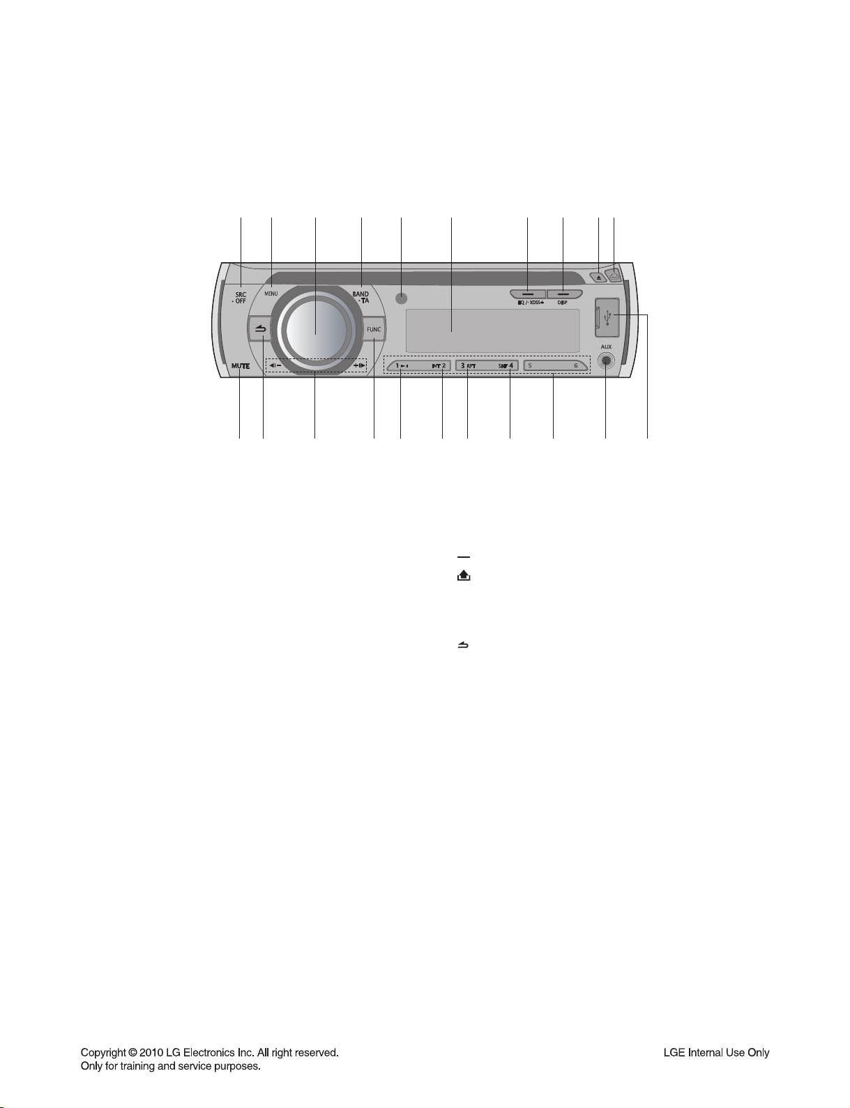
LOCATION OF USERS CONTROLS.................................................................................................................1-5
FIRMWARE UPGRADE METHOD.....................................................................................................................1-6
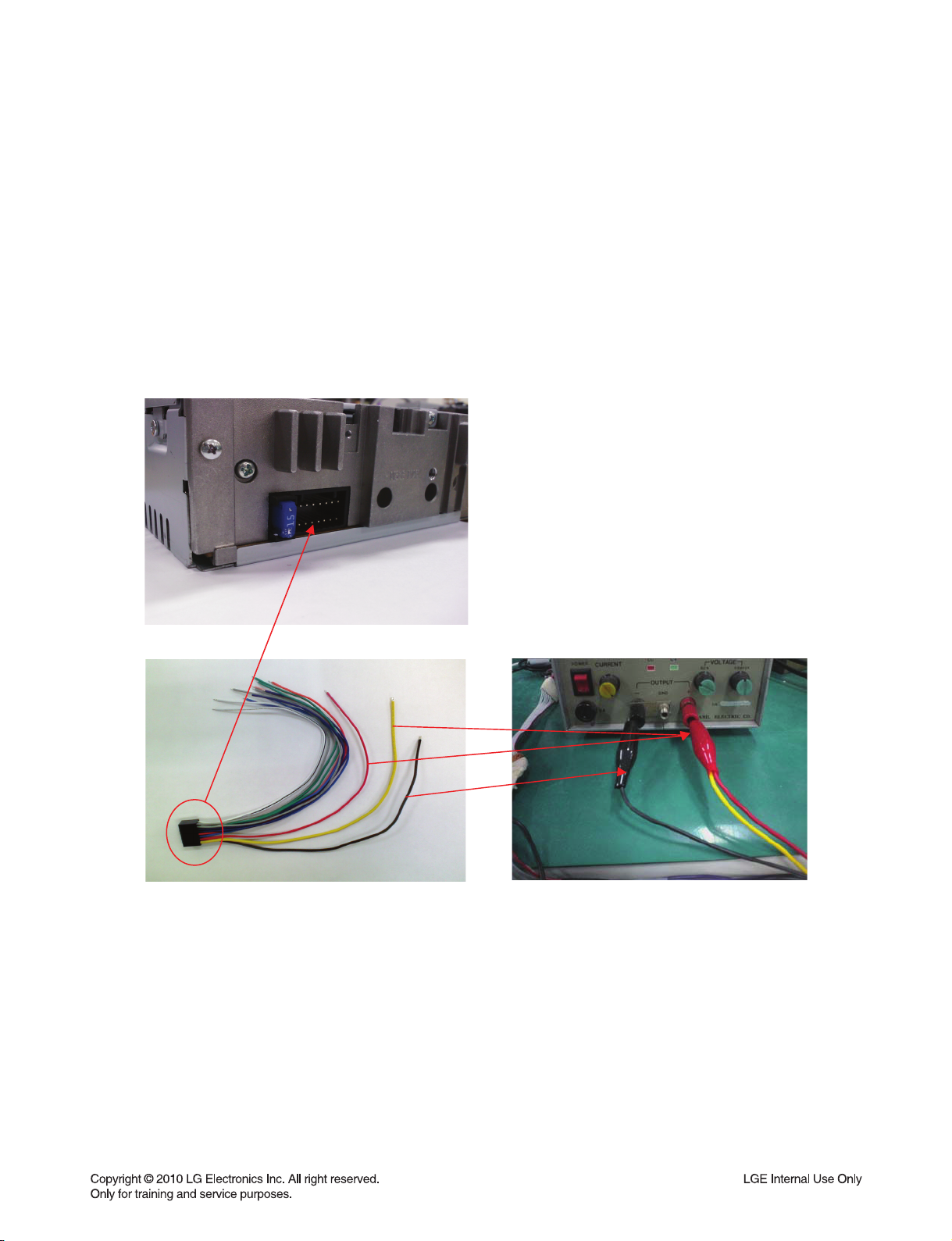
HOW TO CONNECT AUDIO SET TO POWER SUPPLY..................................................................................1-7
SECTION 2 ELECTRICAL
ELECTRICAL TROUBLESHOOTING GUIDE & WAVEFORMS.......................................................................2-1
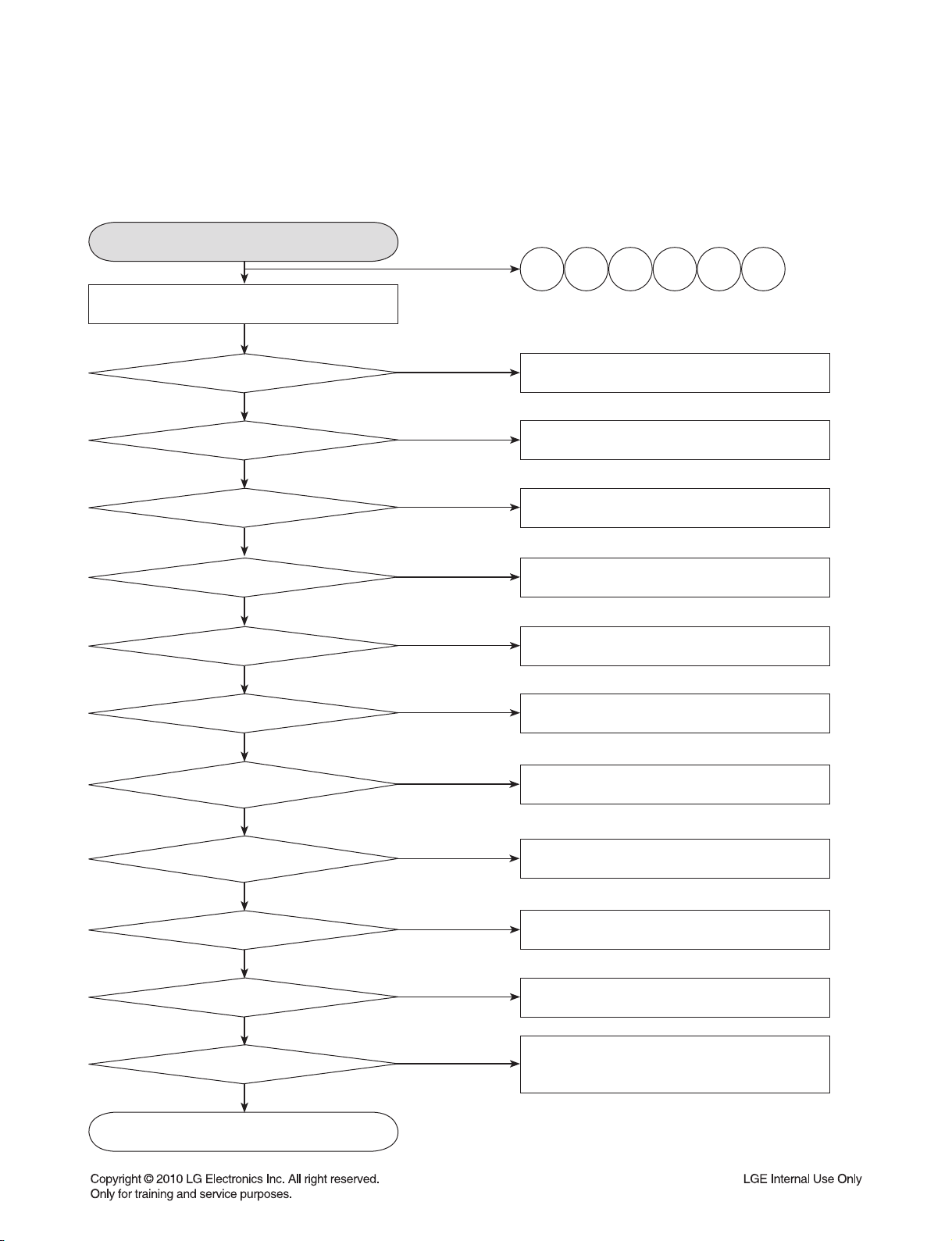
1. SYSTEM CONTROL ERROR CORRECTION FLOW CHART .................................................................2-1
2. SOUND ERROR CORRECTION FLOW CHART......................................................................................2-4
3. DISPLAY ERROR CORRECTION FLOW CHART....................................................................................2-7
4. TUNER ERROR CORRECTION FLOW CHART.....................................................................................2-10
5. CDP ERROR CORRECTION FLOW CHART .........................................................................................2-11
6. USB ERROR CORRECTION FLOW CHART..........................................................................................2-14
7. BLUETOOTH ERROR CORRECTION FLOW CHART (OPTIONAL) .....................................................2-16
8. AUX ERROR CORRECTION FLOW CHART..........................................................................................2-17
• WAVEFORMS ...........................................................................................................................................2-18
• CIRCUIT VOLTAGE CHART ....................................................................................................................2-20
INTERNAL BLOCK DIAGRAM OF ICs ...........................................................................................................2-23
1. IC301 (HA13173AH) ................................................................................................................................2-23
2. IC801 (TB2946HQ) ..................................................................................................................................2-25
3. IC802 (BD3702FV)...................................................................................................................................2-26
4. IC901 (MC5502).......................................................................................................................................2-27
WIRING DIAGRAM...........................................................................................................................................2-29
BLOCK DIAGRAM ...........................................................................................................................................2-31
CIRCUIT DIAGRAMS .......................................................................................................................................2-33
1. MAIN CIRCUIT DIAGRAM.......................................................................................................................2-33
2. FRONT CIRCUIT DIAGRAM ...................................................................................................................2-35
3. CDP CIRCUIT DIAGRAM ........................................................................................................................2-37
PRINTED CIRCUIT BOARD DIAGRAMS ........................................................................................................2-39
1. MAIN P.C.BOARD ...................................................................................................................................2-39
2. FRONT P.C.BOARD ................................................................................................................................2-41
3. CDP P.C.BOARD.....................................................................................................................................2-43
SECTION 3 EXPLODED VIEWS
1. CABINET AND MAIN FRAME SECTION ..................................................................................................3-1
2. MECHANISM(PICK-UP) SECTION ...........................................................................................................3-3
SECTION 4 REPLACEMENT PARTS LIST

1-2
SECTION 1 SUMMARY
SERVICING PRECAUTIONS
1. Always disconnect the power source before:
1) Removing or reinstalling any component, circuit board, module or any other instrument assembly.
2) Disconnecting or reconnecting any instrument electrical plug or other electrical connection.
3) Connecting a test substitute in parallel with an electrolytic capacitor in the instrument.
CAUTION: A wrong part substitution or incorrect polarity installation of electrolytic capacitors may result in an
explosion hazard.
2. Do not defeat any plug/socket B+ voltage interlocks with which instruments covered by this service
manual might be equipped.
3. Do not apply power to this instrument and or any of its electrical assemblies unless all solid-state de-
vice heat sinks are correctly installed.
4. Always connect a test instrument’s ground lead to the instrument chassis ground before connecting
the test instrument positive lead. Always remove the test instrument ground lead last.
1) The service precautions are indicated or printed on the cabinet, chassis or components. When servicing,
follow the printed or indicated service precautions and service materials.
2) The Components used in the unit have a specified conflammability and dielectric strength. When replacing
any components, use components which have the same ratings. Components marked in the circuit diagram
are important for safety or for the characteristics of the unit. Always replace with the exact components.
3) An insulation tube or tape is sometimes used and some components are raised above the printed writing
board for safety. The internal wiring is sometimes clamped to prevent contact with heating components.
Install them as they were.
4) After servicing always check that the removed screws, components and wiring have been installed correctly
and that the portion around the service part has not been damaged. Further check the insulation between
the blades of attachment plug and accessible conductive parts.

1-3
ESD PRECAUTIONS
Electrostatically Sensitive Devices (ESD)
Some semiconductor (solid state) devices can be damaged easily by static electricity. Such components com-
monly are called electrostatically sensitive devices (ESD). Examples of typical ESD devices are integrated circuits
and some field-effect transistors and semiconductor chip components. The following techniques should be used
to help reduce the incidence of component damage caused by static electricity.
1. Immediately before handling any semiconductor component or semiconductor-equipped assembly, drain off
any electrostatic charge on your body by touching a know earth ground. Alternatively, obtain and wear a com-
mercially available discharging wrist strap device, which should be removed for potential shock reasons prior
to applying power to the unit under test.
2. After removing an electrical assembly equipped with ESD devices, place the assembly on a conductive surface
such as aluminum foil, to prevent electrostatic charge buildup or exposure of the assembly.
3. Use only a grounded-tip soldering iron to solder or unsolder ESD devices.
4. Use only an anti-static solder removal device. Some solder removal devices not classified as “anti-static” can
generate electrical charges sufficient to damage ESD devices.
5. Do not use freon-propelled chemicals These can generate electrical charges sufficient to damage ESD de-
vices.
6. Do not remove a replacement ESD device from its protective package until immediately before you are ready to
install it. (Most replacement ESD devices are packaged with leads electrically shorted together by conductive
foam, aluminum foil or comparable conductive materials).
7. Immediately before removing the protective material from the leads of a replacement ESD device, touch the
protective material to the chassis or circuit assembly into which the device will by installed.
CAUTION : BE SURE NO POWER IS APPLIED TO THE CHASSIS OR CIRCUIT, AND OBSERVE ALL
OTHER SAFETY PRECAUTIONS.
8. Minimize bodily motions when handing unpackaged replacement ESD devices. (Otherwise harmless motion
such as the brushing together of your clothes fabric or the lifting of your foot from a carpeted floor can generate
static electricity sufficient to damage an ESD device).
CAUTION. GRAPHIC SYMBOLS
THE LIGHTNING FLASH WITH ARROWHEAD SYMBOL. WITHIN AN EQUILATERAL TRIANGLE,
IS INTENDED TO ALERT THE SERVICE PERSONNEL TO THE PRESENCE OF UNINSULATED
“DANGEROUS VOLTAGE” THAT MAY BE OF SUFFICIENT MAGNITUDE TO CONSTITUTE A
RISK OF ELECTRIC SHOCK.
THE EXCLAMATION POINT WITHIN AN EQUILATERAL TRIANGLE IS INTENED TO ALERT
THE SERVICE PERSONNEL TO THE PRESENCE OF IMPORTANT SAFETY INFORMATION IN
SERVICE LITERATURE.

1-4
SPECIFICATIONS
• GENERAL
Output Power 53 W x 4 CH (Max.)
Power Source DC 12 V
Speaker impedance 4 Ω
Ground System Negative
Dimensions (W x H x D) 178 x 50 x 169 mm (Without Control Panel)
Net Weight 1.22 kg
• TUNER
FM
Frequency Range 87.5 ~ 107.9, 87.5 ~ 108 MHz, 65 ~ 74 or 87.5 ~ 108 MHz
S/N Ratio 55 dB
Distortion 0.7 %
Usable Sensitivity 12 dBµV
AM (MW)
Frequency Range 520 ~ 1720 or 522 ~ 1620 kHz
S/N Ratio 50 dB
Distortion 1.0 %
Usable Sensitivity 28 dBµV
• CD
Frequency Response 20 Hz ~ 20 kHz
S/N Ratio 80 dB
Distortion 0.12 %
Channel Separation (1 kHz) 55 dB
• AUX
Frequency Response 20 Hz ~ 20 kHz
S/N Ratio 80 dB
Distortion 0.1 %
Channel Separation (1 kHz) 45 dB
Max Input Level (1 kHz) 1.1 V
• Bluetooth (optional)
TX POWER 4 dBm
Frequency Range 2402 ~ 2480 MHz
Version Bluetooth Specification 2.0 + EDR
• USB
Version USB 1.1
• Line OUT
Frequency Response 20 Hz ~ 20 kHz
Output Volatage 2 V (Max.)
Subwoofer (optional)
Frequency Selecting 55/85/120 Hz
Output Volatage 2.0 V (Max.)
Designs and specifications are subject to change without notice.

1-5
LOCATION OF USERS CONTROLS
A[SRC] Selects function sources.
[• OFF] Power on/off.
B[MENU] Activates setting menu.
CVolume knob
• Adjusts volume level.
• Confirms the settings.
• Checking tracks or files in CD mode or preset
stations in TUNER mode.
D[BAND] Selects a band.
[• TA] Traffic Announcement (OPTIONAL)
Searches stations that have TA/TP information.
ERemote Sensor
FDisplay window
G[EQ] / [• XDSS+]
Improves sound quality.
H[DISP]
• Press it, you can check the clock time.
• Press and hold it, you can turn off the display
light.
I[S] Releases a disc.
J[ ] Opens the front panel.
K[Mute]
Temporarily stops the sound.
L[ ] Returns to the previous step.
MW❙- / +❙X
Skip / Search / Seek / Tune
N[FUNC] In each mode, sets playback items.
OX❙❙ Plays and pauses playback.
P[INT] Intro scan
Q[RPT] Repeat function
R[SHF] Shuffle
SNumeric buttons
Selects a numbered preset station in TUNER
T[AUX] If connected to other portable player,
you can enjoy musics from it on the unit.
UUSB port
A B C D E F G H IJ
K L M N O P Q R S T U
FRONT PANEL

1-6
FIRMWARE UPGRADE METHOD
[ MAIN AND CD/USB FIRMWARE UPGRADE ]
1. Confirmation of version information
• Change the Source of audio set to tuner.
(Default: tuner)
• Turn power off using power key.
• Press power key for 5 s.
(After power on, continue pressing)
• After 5 s, beep sound rings two times.
Then version information would show up at
display.
• In order to check version of MAIN and CD/USB
system, Press band key.
2. Upgrade Program reading
• Insert update CD or USB in ACC on state and
then
LCS Model
CD : [Reading →File Check →Download?]
USB : [USB Check →Download?]
LCF Model
CD : [Reading →File Check →MN(CD) Down?]
USB : [USB Check →MN(CD) Down?]
is displayed in order.
3. Upgrade start
• In order to start upgrade,
Press LCS Model Preset 1 Key,
LCF Model Play/Pause Key
until “CHECK CD” Display on the LCD.
4. Upgrade progress display
• Upgrade is in progress now.
[ CHECK CD →ERASE →WRITE →I-VRF
→D-VRF ]
5. Upgrade Completion
• When Upgrade finished, the display shows up
“DOWN OK”. After a while, the audio set is
reset automatically.
• Caution!
If power is off on the way of upgrading
firmware, the set can’t be recovered.
Therefore pay lots of attention for power not to
be off.
[ BLUETOOTH FIRMWARE UPGRADE ] - OPTIONAL
1. Insert the burned disc into the LCS700/LCF800, and wait until “DOWNLOAD?” is on LCD.
2. Press “1 ” key for about 1 s, then starts the upgrading process with double beep sound.
3. Upgrading Process is as below
Initial →Link establishment(LINK ESTAB) →DFU initial(DFU INIT.) →
Link establishment (LINK ESTAB) →DFU Preprocess (PREPROCESS) →
Writing →Wait 20Sec →Finalize
4. When Upgrading is completed, the upgrading CD is ejected automatically.
5. When the operation malfunctions, “DFU ERROR” appears on LCD for 2 s,
then the upgrading CD is ejected automatically.
6. Download won’t be proceeded if the existing firmware is identified as same as that of the file downloaded.
If so, “UNNECESSARY” or “UNNEEDED” is on LCD for 2 s, then the upgrading CD is ejected
automatically.
7. It takes 5~6 min to download.

1-7
• It is sufficient only to supply power for upgrade.
• Shown from the right figure, connect yellow line (Battery) and red line (Ignition) to plus and minus terminal
respectively.
• Jack is connected to the audio set via its shapes matched each other.
• We need power supply for operation of audio set (Voltage : 12~15 V Current : Over 2 A)
Before connection between set and power supply, adjust voltage level to 15 V typically (It is okay up to 12 V.)
Power Supply has a variety of shapes and capacity of voltage and current.
At first check these things.
HOW TO CONNECT AUDIO SET TO POWER SUPPLY

1-8

2-1
SECTION 2 ELECTRICAL
ELECTRICAL TROUBLESHOOTING GUIDE & WAVEFORMS
1. SYSTEM CONTROL ERROR CORRECTION FLOW CHART
No power?
Something wrong with the system control?
OK
YES
F301 Inside of CN302
YES
NO
Checked the Fuse?
CN302(1, 2, 3)
YES
NO
Checked the Back up
Vdd and Gnd?
IC301(15, 14)
YES
NO
Checked the Regulator
Back up Vdd ?
IC402(30, 47, 50, 99, 100)
YES
NO
Checked the Main
Micom Vdd?
IC402(20, 51, 97, 98)
YES
YES
NO
Checked the Main
Micom GND?
X401, X402
YES
NO
Checked the Main
Micom X-tal?
IC401, IC402(90)
NO
Checked the Main
Micom Reset?
Q301, R408, IC402(38)
YES
NO
Checked the ACC in?
SW402, IC402(87)
YES
NO
Checked the detachable
switch?(LCF Series only)
IC402(53, 54),
LCS Series : PN901(16, 17)
LCF Series : PN902(9, 10)
YES
NO
Checked the Front
Panel KEY input?
1A 1B 1C 1D 1E 1F
IC402(56)
YES
NO
Checked the Main Micom
B+ Detect ?

2-2
Not available to Remocon?
OK
YES
RC902, R961
YES
NO
Checked the
Remocon Sens Vdd?
YES
R962, IC402(81),
LCS Series : PN901(1)
LCF Series : PN902(24)
NO
Checked the
Remocon Sens line?
1A
Not available to Volume control?
OK
YES
EV901, IC402(82, 83),
LCS Series : PN901(6, 7)
LCF Series : PN902(18, 19)
YES
NO
Checked the
Encoder Volume?
YES
IC402(9, 10), IC802(25, 26)
NO
Checked the
Volume IC Control?
1B
Not available to Key Control?
OK
YES
LCS Series : SW901~SW917
LCF Series : SW901~SW913
YES
NO
Checked the
Tact switch?
YES
IC402(53, 54),
LCS Series : PN901(16, 17)
LCF Series : PN902(9, 10)
NO
Checked the
Key line?
1C

2-3
Not available to Telephone Mute?
OK
YES
ZD499, Q312, Q326, IC402(34)
YES
NO
Checked the Tel
Mute input?
YES
IC402(14, 15), IC802(15)
NO
Checked the
Mute Control?
1D
Not available to ANT(Motor Type) Control?
OK
YES
D430, IC301(12, 13), IC402(33)
NO
Checked the
ANT control?
YES
1E
Not available to Remote(Power AMP) control?
OK
YES
CN302(8), Q320, Q319, IC402(36)
NO
Checked the
Remote control?
YES
1F

2-4
2. SOUND ERROR CORRECTION FLOW CHART
No sounds of All Functions?
Something wrong with the Sound?
OK
YES
IC802(24)
YES
NO
Checked the
E-VR Vdd?
IC802(27)
YES
NO
Checked the
E-VR Ground?
IC802(25, 26), IC402(9, 10)
YES
NO
Checked the
E-VR Control?
IC802(15), IC402(15)
YES
NO
Checked the E-VR
Mute Control?
IC802(1, 2, 3, 4, 5, 6, 7, 9,
18, 19, 20, 21, 22, 23)
YES
YES
NO
Checked the E-VR
Signal in/out?
IC801(1, 2, 8, 13, 18, 24)
YES
NO
Checked the
Power IC Ground?
IC801(23)
NO
Checked the
Power IC Vdd?
IC801(4, 22), IC402(22, 32)
YES
NO
Checked the
Power IC Control?
IC801(3, 5, 7, 9, 11, 12, 14,
15, 17, 19, 21, 23)
YES
NO
Checked the Power
IC Signal in/out?
CN302(11, 12, 13, 14, 15, 16, 17, 18)
YES
NO
Checked
the Main Connector?
2A 2B 2C

2-5
Hearing the Pop Noise?
OK
YES
IC402(14, 15, 32), IC802(15),
IC801(22), Q603, Q604, Q605, Q606, Q608
NO
Checked the
Mute Contorl?
YES
2A
No Sound External AMP?
OK
YES
IC802(18, 19, 20, 21, 22, 23)
NO
Checked the
Line Out Signal?
YES
Q603, Q604, Q605, Q606, Q608, IC402(15)
NO
Checked the Line Out
AMP Mute Control?
YES
JK601
NO
Checked the Line Out
AMP Signal in/out?
YES
2B
No output Beep sound?
OK
YES
YES
IC402(80), IC802(14)
NO
Checked the
Beep Control?
2C

2-6
■CAUTION - Tip for repair
Before exchange power amp IC(TB2946) for no audio problem, you have to check
below list.
1. Check VCC (pin 20, 6) & GND
2. Check input pin 11, 12, 14, 15
3. Check Standby, pin 4
: Follow the below list.
4. Check Mute function, pin 22
: Follow the below list.
5. Check Ripple pin 10.
: Normally it is high (about 10 V)
6. Re-soldering all the pin of IC.
: Prevent crack of solder line.
* Keep changed IC, We request that you send it to HQ.
Stand-by Power Sound Voltage
ON OFF OFF 0 to 1.5
OFF ON ON 3.5 to 6 V
Mute Sound Voltage
ON OFF 0 to 1.5
OFF ON 3.5 to 6 V
RL
RL
RL
11
9
8
7
5
2
3
17
18
19
21
24
23
12
15
14
120 6
RL
IN1
IN2
IN3
IN4
13
C1
C1
C1
C1
PRE-GND
10 25 22
OUT1 +
+
+
+
-
-
-
-
()
PW-GND1
OUT1 ( )
OUT2 ( )
PW-GND2
OUT2 ( )
OUT3 ( )
PW-GND3
OUT3 ( )
OUT4 ( )
PW-GND4
OUT4 ( )
TAB VCC1 VCC2
C3
C4
C2
: PRE-GND
: PW-GND
STBYRIP MUTE
C5
16
C6
4
OFF-SET
DET
MUTE
PLAY
5 V
R1
AC-GND
Picture 1) Power IC desc.

2-7
3. DISPLAY ERROR CORRECTION FLOW CHART
No Display or Some Display is broken?
Something wrong with the Display?
3A 3B
OK
YES
LCS Series : IC901(56)
LCF Series : LCD901(7)
YES
NO
Checked the LCD
Driver Vdd?
YES
LCS Series : IC901(60)
LCF Series : LCD901(10)
NO
Checked the LCD
Driver Ground?
YES
LCS Series : IC901(57), IC402(79)
NO
Checked the LCD
Driver Reset?
YES
LCS Series : IC901(61)
LCF Series : LCD901(6)
NO
Checked the LCD
Driver OSC?
YES LCS Series : IC402(44, 46, 74, 79),
PN901(2, 8, 18, 19),
IC901(57, 62, 63, 64)
LCF Series : IC402(44, 46, 74, 79),
PN902(7, 8, 17, 23),
LCD901(2, 3, 4, 5)
NO
Checked the LCD
Driver data interface?
YES
LCS Series : IC901(1~55),
LCD, Check the short
NO
Checked the LCD to
LCD Driver line?

2-8
Not available to illumination with button?
OK
YES
CN302(7), IC301(9)
YES
NO
Checked the Dimmer
control input?
YES
IC301(4), Q303, IC402(61)
NO
Checked the
RED LED Vdd?
YES
YES
LCS Series : LD921~LD945
LCF Series : LD921~LD936
NO
Checked the
RED LED?
OK
YES
IC301(4), Q304, IC402(43)
NO
Checked the
BLUE(GREEN) LED Vdd?
YES
LCS Series : LD951~LD975
LCF Series : LD951~LD966
NO
Checked the
BLUE(GREEN) LED?
3A

2-9
Not available to LCD Lighting control?
OK
YES
CN302(7), IC301(9)
NO
Checked the Dimmer
control input?
YES
3B
YES
IC301(4), Q302, IC402(49)
NO
Checked the
White LED Vdd?
YES
LCS Series : LD991, LD992
LCF Series : LD990~LD993
NO
Checked the
White LED?

2-10
4. TUNER ERROR CORRECTION FLOW CHART
Not available to Tuner?
Something wrong with the Tuner system?
OK
YES
IC101(6, 22)
NO
Checked the
Tuner Vdd?
YES
IC301(10, 11), IC402(40), D417
NO
Checked the Tuner
Vdd control?
YES
IC101(5, 10, 17, 23)
NO
Checked the
Tuner Ground?
YES
IC802(15), IC402(15)
NO
Checked the E-VR
Mute Control?
YES
IC101(18, 19), IC402(3, 4)
NO
Checked the
I2C data?
YES
IC101(8, 9)
NO
Checked the
Audio Signal?
YES

2-11
5. CDP ERROR CORRECTION FLOW CHART
No Loading?
Something wrong with the CD Player?
OK
YES
CN520(14, 12)
YES
NO
Checked the CD Vdd?
YES
IC501(4, 5, 7, 9, 12, 44, 49, 51, 74, 77, 81,
102, 104, 116, 117)
NO
Checked the CD
DSP Ground?
YES
IC504(7, 8, 20)
NO
Checked the Motor
DRV Vdd?
YES
CN520(19)
NO
Checked the CD
DSP Reset?
YES
X501(4.2336 MHz)
NO
Checked the CD
DSP X-tal?
YES
CN506(2)
NO
Checked the Disc in
load switch?
YES
CN520(21, 23)
NO
Checked the Loading
Motor Control?
YES
CN506(1)
NO
Checked the 12/8 cm
sense switch?
Fig 1, 2
Fig 3, 4
Fig 1, 2
5A 5B 5C
Table of contents
Other LG Car Receiver manuals