Linear AT7120 User manual

ADVANCED TV
LINE
Model AT7120
120W ATSC UHF Transmitter
OWNERS MANUAL
Linear Industries Incorporation
www.linear-tv.com
Made in USA

AT7120 Owner Manual Rev. 1.1 –March 2009 2/76
AT7120
120W UHF 8VSB-ATSC TRANSMITTER
ADVANCED TV LINE
Owner Manual
Table of Contents
User Notices and WARNINGS .................................................................................................. 3
Section 1 –AT7120 General Description................................................................................... 6
Section 2 –Control Set............................................................................................................ 15
Section 3 –8VSB Modulator and Master Clock....................................................................... 22
Section 4 –IF/UHF up-converter............................................................................................. 26
Section 5 –UHF ATSC Exciter................................................................................................ 31
Section 6 –UHF ATSC Amplifier............................................................................................. 35
Section 7 –Power Supply........................................................................................................ 40
Section 8 –DC/DC Converter.................................................................................................. 47
Section 9 –Memory Interface.................................................................................................. 48
Annex A –AT7120 Operational Software................................................................................ 49
Annex B –Checking the RF Power LDMOS Transistors......................................................... 72
Annex C –Typical Final Test Reports Results ........................................................................ 73

AT7120 Owner Manual Rev. 1.1 –March 2009 3/76
User Notices and WARNINGS
USER NOTICES
IT IS VERY IMPORTANT TO READ THE FOLLOWING MANUAL SECTIONS PRIOR TO
OPERATION OF THIS TRANSMITTER!
Notice 1
The transmitter main operating voltage setting is marked on the rear of the chassis.
Notice 2
The transmitter operating frequency is set from the factory.
Notice 3
For adjusting the RF output power setting a qualified technician should always employ the use of an RF
Wattmeter and a calibrated dummy load.
Notice 4
Should accident or injury occur to the personnel engaged in the installation, operation, or service of the
equipment should seek proper medical attention. It is advisable that such personnel have familiarity
with first-aid practices.
Notice 5
To call our technical support center or for other customer service issues at Linear Inc, refer to the
following number: 847 428-5793, or e-mail to broadcast@linear-tv.com
Notice 6
If you experience some specific difficulty and the technical information available in this manual is not
enough to help you, do not hesitate to call LINEAR technical support center.
Notice 7
The technical information presented on this manual is sole intellectual propriety of LINEAR
INDUSTRIES Inc. Reproduction of this document in full or partial is prohibiting without written
authorization. This document is legally protected by the copy rights laws.
WARNING!
THE VOLTAGES AND CURRENTS IN THIS EQUIPMENT COULD BE DANGEROUS. PERSONEL
MUST, AT ALL TIMES, OBSERVE SAFETY WARNINGS, INSTRUCTIONS, AND ANY
REGULATIONS.

AT7120 Owner Manual Rev. 1.1 –March 2009 4/76
THIS OWNER’S MANUAL IS INTENDED AS A GENERAL GUIDE FOR TRAINED AND
QUALIFIED PERSONNEL WHO ARE AWARE OF THE DANGERS THAT ARE INHERENT IN
THE HANDLING AND OPERATION OF POTENTIALLY HAZARDOUS ELECTRICAL AND
ELECTRONIC CIRCUITS. IT IS NOT THE INTENT OF THIS MANUAL TO PROVIDE A
COMPLETE SET OF SAFETY INSTRUCTIONS OR PRECAUTIONS THAT SHOULD ALREADY
BE UNDERSTOOD BY TRAINED OR EXPERIENCED PERSONNEL IN USING THIS OR OTHER
TYPES OF ELECTRONIC EQUIPMENT.
THE INSTALLATION, OPERATION, AND MAINTENANCE OF THIS EQUIPMENT INVOLVE
RISKS TO PERSONNEL AND ALSO TO THE EQUIPMENT. LINEAR, INC. SHALL NOT BE
RESPONSIBLE FOR INJURY OR DAMAGE THAT IS THE RESULT OF IMPROPER
PROCEDURES OR USE BY PERSONS IMPROPERLY TRAINED OR LACKING THE
KNOWLEDGE TO PERFORM ASSOCIATED TASKS.
ALL LOCAL CODES FOR BUILDING, SAFETY, FIRE, OR RELATED STANDARDS MUST BE
OBSERVED. CONSULT LOCAL AUTHORITIES FOR THE STANDARDS FOR THE AREA OR
REGION WHERE THE EQUIPMENT WILL BE INSTALLED AND PUT IN USE.
WARNING!
AT ALL TIMES DISCONNECT AC/MAINS POWER BEFORE OPENING COVERS, DOORS,
ENCLOSURES, PANELS, OR PROTECTIVE SHIELDS THAT EXPOSE LIVE CIRCUITS. NEVER
PERFORM MAINTENANCE, MAKE ADJUSTMENTS, OR SERVICE THE EQUIPMENT WHEN
ALONE OR FATIGUED.
WARNING!
IF ELECTROLYTIC OR OIL FILLED CAPACITORS ARE UTILIZED IN THE EQUIPMENT AND
THE COMPONENT APPEARS LEAKY, OR IS BULGING, OR IF THE CASE OR COVERING OF
THE COMPONENT APPEARS DAMAGED OR DISTRESSED ALLOW SUFFICIENT TIME FOR
THE UNIT TO COOL and FULLY DISCHARGE BEFORE SERVICING. SERVICING HOT OR
LEAKY CAPACITORS CAN CAUSE A RUPTURE OF THE CASE AND POSSIBLE INJURY.
Returns and Exchanges
Equipment (Damaged or undamaged) should not be returned without written approval and a
Merchandise Return Authorization (MRA Number) from your Linear Sales representative or Linear
Customer Service. Special shipping instruction will be provided which will assure proper handling.
The circumstances and reasons for the return must be included in the request for return. Equipment that
is special or “custom” ordered may not be returnable. In situations where return or exchange is at the
request of the customer a restocking fee may be charged. All returns must be sent freight prepaid and

AT7120 Owner Manual Rev. 1.1 –March 2009 5/76
properly insured by customer. When communicating with Linear please refer to your Order or Invoice
Number.
Unpacking
Use care when unpacking the equipment. First perform a visual inspection of the item(s) to determine if
any damage occurred during shipment. Be sure to retain all the shipping materials (crates and boxes or
cartons) until such time that it has been determined that the received equipment arrived undamaged.
Find all PACKING LISTS and keep them to assist in locating and identifying any components or
assemblies that may have been removed for safe. Make sure that all shipping straps, supports and
packing materials are completely removed from the equipment prior to initialization and use.

AT7120 Owner Manual Rev. 1.1 –March 2009 6/76
Section 1 –AT7120 General Description
The ATSC DTV transmitter model AT7120 is part of the ADVANCED TV line, having modular
construction meeting EIA 19”rack standards, and is composed for the following modules:
01 Main Control unit - CIM3297
01 Keypad - CIM3003
01 Display LCD 20 columns x 02 lines - CIM3004
01 Memory interface - CIP8421
01 1Mbits memory card –CIP8421
01 UHF ATSC Exciter- Module 4407
01 up-Digital Converter - Module 4492
01 Power Supply - Module 4401 (versions M110/M220/B220)
01 8VSB Modulator and Master Clock Generator - Module 4549
01 DC/DC Converter (+2.5V and +5V) –Module 4567
02 UHF ATSC Amplifier –Module 4442
01 OCXO –Module 4292
When AT7120 is a TRANSMITTER that can be installed with or without a 6 pole elliptical filter on its
RF output. In this application, the overall performance of the unit will meet or exceed the FCC
requirements for out of channel spurious emission. Please refer to Annex C.

AT7120 Owner Manual Rev. 1.1 –March 2009 7/76
AT7120 Block Diagram
+28V
RELIGADO
UHF ATSC EXCITER
MODULE 4407
+8V+15V
KEYBOARD
CIM3003
LINEAREQUIPAMENTOS ELET RÔNICOS
DISPLAY
CIM3004
RESTART
RFOUT
ALARME DE
TEMPERATURA LEITURA DE
POTÊNCIA DIRETA
FAN
FILTER FAN
CIM6646 +24V
IN OUT
EXC.TEMPERATURE
PA1 TEMPERATURE
PA2 TEMPERATURE
ALARMS
SHUT DOWN 1
CONTROL UNIT
CIM3297
(CIP8231)
MAIN POWER SUPPLY
MODULE 4401
ID
CURRENT
READING +28V
READING +18V
READING -18V
READING +9V
READING
+18V-18V
+9V
+28V
FIXO
+28V
RES.
1 SUBORDINATE
POWER SUPPLY
MODULE 4402
SHUT DOWN 1
+28V
FIXO
AC FAN
+32V
(VA) +32V
(VB) TEMP
PA 1 PA1
TEMP
ALARM
ID1
READ ID2
READ
+28V
FIXO
UHF ATSC
AMPLIFIER
PA1
MODULE 4442
IN OUT
+32V
(VA) +32V
(VB)
1 SUBORDINATE
POWER SUPPLY
PA1
TEMP
8VSB
MODULATOR AND
MASTER CLOCK UHF UPCONVERTER
MODULE 4492
+18V-18V
RFOUT
SW2
TEMP
ENABLE Q DAC
ENABLE I DAC
CLOCK DAC
DATA DAC
ALC
+28V
FIXO
CLOCK PLL
LOCK DETECT
MODULE 4549
+5V+2.5V +18V-18V
10MHz
OCXO
MODULE 4281
RD
ENA
CLK
DIN
DO
LD
CONTROL UNIT
+28V
MODULE 4567
DC CONVERTER
+5V+2.5V
MEMORY
MEMORY
CARD
CARD
CIP8421
CIP8421
MEMORY INTERFACE
MEMORY INTERFACE
CIP8437
CIP8437
DCLK
ASDI
CS
DATA
FROM
CONTROL
UNIT
110 / 220V
MONOPHASIC / BIPHASIC
ON/OFF
SWITCH
5A / 220V
10A / 110V
FUSE
FUSE 5A / 220V
10A / 110V
120Wrms
RF OUT
RF
PW REF
PW
+15V
REFLT
IN OUT
MODULE
4166
FPB
MODULE
4252
310M IN
ASI IN
EXT. REF. IN
EXCITER FORWARD POWER
FORWARD POWER
REFLECTED POWER
I1 MAIN POWER SUPPLY
PA1 CURRENT ID1
PA1 CURRENT ID2
PA2 CURRENT ID3
PA2 CURRENT ID4
+28V MAIN POWER SUPPLY
+18V MAIN POWER SUPPLY
-18V MAIN POWER SUPPLY
+9V MAIN POWER SUPPLY
+32V 1 SUBORDINATE POWER SUPPLY
+32V 2 SUBORDINATE POWER SUPPLY
READINGS
MASTER CLOCK LOCK DETECT
+5V
QIN
IIN
+32V
READ
ENABLE
DATA PLL
SW1
DCLK
ASDI
CS
DATA
TO MEMORY
INTERFACE
RD
ENA
CLOCK
DIN
DO
LD
MODULATOR
÷
OUT 1
OUT 2
IN
MODULE 4442
IN OUT
+32V
(VA) +32V
(VB)
2 SUBORDINATE
POWER SUPPLY
PA2
TEMP
UHF ATSC
AMPLIFIER
PA2
Σ
IN 1
IN 2
OUT
2 SUBORDINATE
POWER SUPPLY
MODULE 4402
SHUT DOWN 2
+28V
FIXO
+32V
(VA) +32V
(VB) TEMP
PA 2 PA2
TEMP
ALARM
ID3
READ ID4
READ +32V
READ
AC FAN
SHUT DOWN 2
RS232
TELESUPERVISION
CONTROL
UNIT

AT7120 Owner Manual Rev. 1.1 –March 2009 8/76
Module 4549
8VSB Modulator
The 8VSB modulator automatically recognizes the incoming transport stream as either SMPTE310M or
ASI. The transport stream input utilizes the BNC connector located on the rear panel of the unit. The
modulated output signal of this module is composed by two IF orthogonal carriers termed; signals (I)
and (Q). The central frequency of the 8VSB modulated IF signal is 18.83339MHz. The signal
processing and modulation performed on this module follows the ATSC recommendation A/53 E.
This module also performs the non-linear corrections that might be necessary to enhance the equipment
efficiency to meet FCC spurious emissions requirements. In this case, an RF output filter is required.
The recommended linear equalization is also automatically performed in this module.
Master Clock
The master clock unit generates signals utilizing a Voltage Controlled Oscillator and Phase Locked
Loop at 172.16MHz. The PLL is locked at 10MHz reference, externally or internally generated. This
signal provides the time base for the 8VSB modulator.
Module 4492
IF to UHF up-Converter
The IF carries the orthogonal (I) and (Q) signals generated in module 4549, (8VSB Modulator), which is
then routed to the up-converter module. The output signal of this module is set on the FCC/UHF
operational 6MHz channel of the transmitter AT7120.
Inside the converter the modulated IF band is mixed with the continuous wave local oscillator LO. As a
result of this mixing, the IF translation to the UHF band is performed. The LO is a free oscillator, that
has its frequency locked via PLL. The LO/PLL is generated by a 10MHz OCXO (oven controlled
crystal oscillator), or provided by an external reference signal.
Module 4281
10MHz reference automatic switching
Both circuits; the 8VSB modulator and the up-converter, share the same reference signal source. The use
of the same reference signal creates perfect synchronization and stability during the DTV transmission
process. The internal 10MHz signal is obtained from an OCXO oscillator with a stability of 0.3ppm. An
external 10MHz signal can be used as the reference signal; a GPS signal for instance. The external
reference input is a BNC connector located on the rear panel of the unit. In the absence of this external
source, the unit automatically utilizes the internal 10MHz source generated by the OCXO.

AT7120 Owner Manual Rev. 1.1 –March 2009 9/76
Module 4407
60W UHF band multistage amplifier
The IF modulated signal (previously converted into UHF) is amplified by a 60W UHF amplifier. This
amplifier uses transistors built with LDMOS technology operating in a class AB configuration, which
provides excellent efficiency and linearity. The RF OUT connector of the unit provides the high power
RF output.
RF Output monitoring
Module 4407 detects the direct and reverse RF power present on the RF OUT connector of the unit. The
detected information is then converted to correspondent DC levels before being routed to the master
control unit, where it is processed and displayed at the front panel LCD screen in watts.
Module 4442
AT7120 transmitter has two Modules 4442 connected in parallel, which work as digital TV end
amplifiers in all UHF band. The amplifier is made of the following components:
Input Coupler
The input RF coupler equally divides the UHF signal present in the input connector for the two
amplification cells, maintaining 50Ω impedance.
Cell A –35W Amplifier
The amplification cell A is obtained by a Push-Pull 35W amplifier, class AB. Transistor T1 is in this
cell. The polarization circuit of cell A is made of a VGS timer circuit with temperature compensation,
differential amplifier and gate impedance reducer.
Cell B –35W Amplifier
Just as cell A, cell B’s amplification is obtained by a Push-Pull 35W amplifier, class AB. Transistor T2 is in this
cell. The polarization circuit in cell B also is made of a VGS timer circuit with temperature compensation,
differential amplifier and gate impedance reducer.
Output Coupler
It is a hybrid coupler built with a special semi-rigid coaxial cable, better known as “wireline”. This type
of cable has 2 internal conductors interlinked; this set has the characteristics of a hybrid coupler. As the
input coupler, this coupler also has four gates (input/output; isolated, -3dB 0˚, -3 dB 90˚).
Temperature Alarm
Module 4442 has a protection circuit that disarms the module in case the temperature rises above 65˚ C.
This circuit is basically made of thermal sensor S1, DC amplifier and voltage comparator CI-1.

AT7120 Owner Manual Rev. 1.1 –March 2009 10/76
CIM3297
Control unit card
The digital management of the DTV AT7120 transmitter is done by the control unit card, CIM3297.
This control unit uses an A128 microcontroller programmed in assembler language. The unit process
data regarding the following operational parameters:
Warns of signal lock failure of the PLL in the up-converter.
Warns of excessive temperature of the 60W amplifier.
Monitors and displays the RF direct and reflected powers of the 60W amplifier, muting the transmission
in case of extreme levels.
Displays DC current levels of the main power supply module.
Process and displays power supply voltage(s).
Sets in the operational channel of the Up-converter unit and transmits power levels via ALC. Sets and
monitors the operational channel frequency in the up-converter unit as well as the transmit power levels
which is controlled by the automatic level control circuits.
The control unit is directly connected to a keypad and LCD screen, both located on the front panel of the
transmitter AT7120. Numerous parameters can be set via the keypad and monitored by the LCD screen.
The same functions can be performed via RS232 HyperTerminal connection.
Module 4401
Power Supply
The power supply module is a switching power supply type, utilizing a half-bridge topology. A control unit
monitors the power supply output and adjusts to varying load to maintain a nominal +32 VDC. The voltage and
current data is provided to the control unit card for display on the LCD screen.

AT7120 Owner Manual Rev. 1.1 –March 2009 11/76
AT7120 External Interfaces
Fig.1.2: AT7120 Front View

AT7120 Owner Manual Rev. 1.1 –March 2009 12/76
Fig.1.3: AT7120 Rear Panel View
Power Switch
ID Tag
External 10MHz
Reference Input
Main Fuse
ASI/SMPTE310M Transport
Stream Input
AC Power Cord
(DB-9) RS232
Hyper-terminal Interface
Hot Air Outlets
GND
RF Output
Connector
Internal DB-9
Not Used
AT7120 Owner Manual Rev. 1.1 –March 2009 13/76
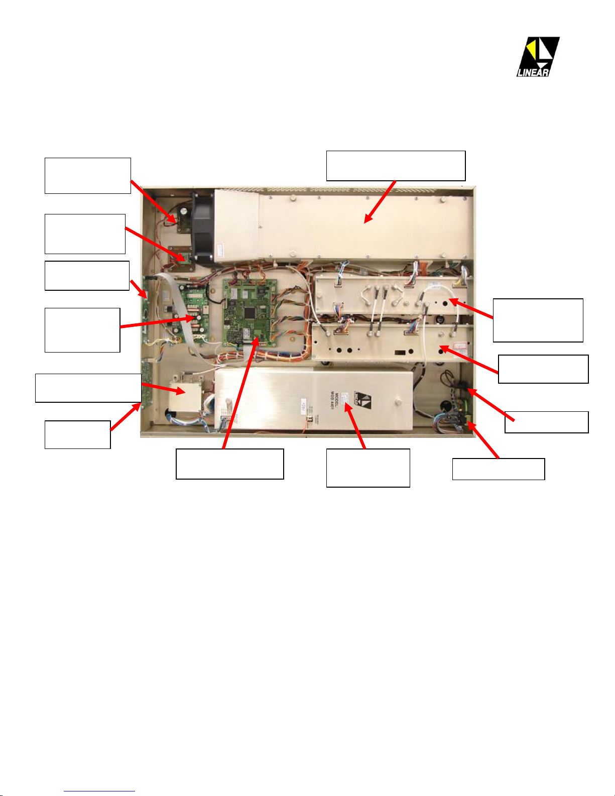
AT7120 - Modules and Parts Displacement
Fig.1.4: AT7120 Modules and Parts displacement
Key Pad
CIM3003
RF Power Amplifier
Module 4407
LCD Screen
CIM3004
Memory Card &
Interface
CIP 8437
DC/DC
Converter
Module 4567
DC Fan Filter
CIM6646
Digital Control Card
CIM3297/CIP8231A
+32V Power
Supply Module
4401
Ref. 10MHz OCXO
Module 4281
Power Switch
Fuse & GND
Up Converter
Module 4492
8VSB Modulator &
Master Clock
Module 4549
AT7120 Owner Manual Rev. 1.1 –March 2009 14/76
AT7120 - 120W ATSC UHF Transmitter - Technical
Specifications
Table XX: AT7120 Technical specifications
Electrical
Main
220 VAC, bi phase, 50-60 Hz. standard
Consumption
400W @ 120W RMS/RF
Power Factor Correction, FPC.
Included
Signal Input
Transport Stream Input
ATSC/MPEG2, compliant to
SMPTE310M
Input Data Rate
19.39 Mbps
External Reference Signal
10MHz. (0 to +10 dBm).
Input Connector
75Ω (BNC),
Reference Input Connector
50Ω (BNC),
RF
Modulation Mode
8VSB.
IF
18.833916 MHz.
Channel Bandwidth
6MHz.
Test Signal
PRBS
Frequency Range
UHF. C14 to Ch53, (3 bands).
Frequency Step
1 Hz. ± 220kHz
Symbol Rate
10.76 MSymbol/sec.
Digital/Analog Converter
16 bit
Linearization Pre-Correction
Included
Pilot frequency stability overall
± 4.6 ppm.
Initial tolerance
± 1.0 ppm.
Vs. temperature in operating temperature range (steady
state)
± 10 ppb.
Holdover 24 hours, full temp. range
± 12 ppb.
24 hours drift (after 30 days)
± 1.0 ppb.
Long term stability over 15 years
± 3.5 ppm.
Peak to peak frequency response
0.15 dB.
Peak to peak group delay response
10 ns.
Phase noise
≤ -104 dBc/Hz @ 20kHz offset.
Conducted spurious and harmonics
< -60 dBc, FCC 47 Part 74.
Radiated spourious and harmonics
< -80 dBc, FCC 47 Part 74.
MER (Modulation Error Rate)
≥ 29 dB (transmitter output) typical.
RF output connector
N
Communication
Hyper-terminal
RS232 (DB-9)
External Command –ON/OFF
(DB-9)
Mechanical
Air speed over drawers
50 ft/minute.
Dimensions
5UR (H), 19”(W), 26”(D)
Weight
Gross: 110 lb.

AT7120 Owner Manual Rev. 1.1 –March 2009 15/76
Section 2 –Control Set
Functional Description
The digital control is responsible for all management of AT7120 transmitter.
This unit Monitors and assures the system is operating within acceptable parameters and provides user control
access via key pad located on the front panel, or via RS232 hyper-terminal.
Its main attributions are:
Warns of signal lock failure of the PLL in the up-converter.
Warns of excessive temperature of the 60W amplifier.
Monitors and displays the RF direct and reflected powers of the 60W amplifier, muting the
transmission in case of extreme levels.
Displays DC current levels of the main power supply module (I1).
Process and displays power supply voltage(s).
Sets in the operational channel of the Up-converter unit and transmits power levels via ALC.
Sets and monitors the operational channel frequency in the up-converter unit as well as the
transmit power levels which is controlled by the automatic level control circuits.
The control unit is directly connected to a keypad and LCD screen, both located on the front panel of the
transmitter AT7120. Numerous parameters can be set via the keypad and monitored by the LCD screen.
The same functions can be performed via RS232 HyperTerminal connection.
Control unit block diagram
CONTROL
UNIT
CIP8231
(CIM3297)
MICROCONTROLLER
DISPLAY
CIM3004
KEYBOARD
CIP8002
(CIM3003)
EXCITER FORWARD POWER READING
EXCITER REFLECTED POWER READING
EXC.20W ID CURRENT READING
VOLTAGES SUPPLY READINGS
RS232 REMOTE CONTROL
EXTERNAL FUNCTIONS
Fig.2.1: Control unit general block diagram

AT7120 Owner Manual Rev. 1.1 –March 2009 16/76
The printed circuit board CIP8231 is referred to as the control unit, and provides the major functionality
of the AT7120 digital control unit.
For a better understanding of the functioning of this board please refer to Fig.2.1 “Control unity general
block diagram”, above, which depicts the main components and connections. Figure 2.2, below, shows
a detailed schematic of CIP8231 including connector pin layout.
01 control unit board - CIP8231 (CIM3297)
01 keypad board - CIP8002 (CIM3003)

AT7120 Owner Manual Rev. 1.1 –March 2009 17/76
01 20 x 2 LCD display board - CIM3004
CIP8231 Connections
(BK) SW2 PIN 3 –CON 6 –CIP8388 –MOD. 4492 –UHF UPCONVERTER
(GR) TEMPERATURE ALARM PIN 4 –CON-5 –CIP8209 –MOD.4408 –UHF AMPLIFIER
(GY) RESTART PIN 6 –CON-8 –CIP8111 –MOD. 4401 –POWER SUPPLY
CON-1
BL
7
CON-2
1 9
9
1
36CON-7 CON-8 CON-9
1
GND
VCC
DA1
DA2
+15V
IRQ
CON-3
1
6
CON-4
8
CON-5
8
1
CON-6
8
1
PA21
PA31
PA41
PA51
PA61
PA71
1
PA02
PA12
PA22
PA32
PA42
PA52
PA62
PA72
PB01
PB11
PB21
PB31
PB41
PB51
PB61
PB71
PB72
PB62
PB52
PB42
PB32
PB22
PB12
PB02
GND
TX
RX
PC6
PC5
GND
A16
A15
A14
A13
A12
A11
A10
A09
GND
A08
A07
A06
A05
A04
A03
A02
A01
CI -7
LM7805
CI-1
1 2 3
TPO-1
AJUSTE
LUM. DISPLAY
XTAL1
1
14
SCL
SDA
PM4
PM3
PJ1
PJ0
16MHz DTR
CTS
RX
TX
GND
RTS
DCD
CON-11
1
6
CON-10
1
7
J1 VM
BDM IN
MC34064
LM358
CI -4
MCS12A128BMCS12A128B
MC9S12A128B
Q1
BCX53
CON-12
1
1
.
DS229
..
RS232
RS485
J4
J5
.
DS229
CI -6
CI-2
.
CI-3
.
(GY) DATA PLL PIN 6 –CON-3 –CIP8388 –MOD. 4492 –UHF UPCONVERTER
A
B
GND
(WH) RX RS232 PIN 2 –CON DB9 RS232 –REAR PANEL
(RD) TX RS232 PIN 3 –CON DB9 RS232 –REAR PANEL
(SH) GND RS232 PIN 5 –CON DB9 RS232 –REAR PANEL
(WH) GND PIN 1 –CON-6 –CIP8388 –MOD. 4492 –UHF UPCONVERTER
(BL) +15V PIN 1 –CON-13 –CIP8111 –MOD. 4401 –POWER SUPPLY
(GR) +8V PIN 1 –CON-11 –CIP8111 –MOD. 4401 –POWER SUPPLY
(YL) ENABLE QDAC PIN 8 –CON 6 –CIP8388 –MOD.4492 –UHF UPCONVERTER
(GY) SW1 PIN 4 –CON 6 –CIP8388 –MOD.4492 –UHF UPCONVERTER
(OR) CLOCK DAC PIN 7 –CON-6 –CIP8388 –MOD.4492 –UHF UPCONVERTER
(OR) LD CLOCK GENERATOR PIN 1 –CON-7 –CIP8358 –MOD. 4549 –8VSB MODULATOR
(BK) DATA OUT PIN 3 –CON-2 –CIP8357 –MOD. 4549 –8VSB MODULATOR
(BR) ENABLE PLL PIN 5 –CON-3 –CIP8388 –MOD. 4492 –UHF UPCONVERTER
(YL) CLOCK PLL PIN 7 –CON-3 –CIP8388 –MOD. 4492 –UHF UPCONVERTER
(VL) LOCK DETECT PIN 8 –CON-3 –CIP8388 –MOD. 4492 –UHF UPCONVERTER
(OR) DATA IN PIN 2 –CON-2 –CIP8357 –MOD.4549 –8VSB MODULATOR
(RD) MODULATOR CLOCK PIN 4 –CON-2 –CIP8357 –MOD.4549 –8VSB MODULATOR
(GR) MODULATOR ENABLE PIN 5 –CON-2 –CIP8357 –MOD.4549 –8VSB MODULATOR
(VL) MODULATOR READ PIN 6 –CON-2 –CIP8357 –MOD.4549 –8VSB MODULATOR
(VL) DATA DAC PIN 6 –CON-6 –CIP8388 –MOD.4492 –UHF UPCONVERTER
(YL) TX ON PIN 3 –CON DB9 –REAR PANEL
(RD) ENABLE IDAC PIN 9 –CON 6 –CIP8388 –MOD. 4492 –UHF UPCONVERTER
(YL) BACK LIGHT DISPLAY POINT A –LCD DISPLAY–CIM3004
(YL) CS MEMORY PIN 4 –CON-2 –CIP8437 –MEMORY INTERFACE
(YL) ROW1_KEYBOARD PIN 1 –CON-3 –CIP8002 –KEYBOARD
(BL) LINE1_KEYBOARD PIN 6 –CON-3 –CIP8002 –KEYBOARD
(GY) ROW3_KEYBOARD PIN 3 –CON-3 –CIP8002 –KEYBOARD
(OR) DCLK_MEM PIN 6 –CON-2 –CIP8437 –MEMORY INTERFACE
(OR) LINE3_KEYBOARD PIN 4 –CON-3 –CIP8002 –KEYBOARD
(WH / RD) ALC PIN 2 –CON-6 –CIP8388 –MOD. 4492 –UHF UPCONVERTER
(RD) ASDI_MEM PIN 5 –CON-2 –CIP8437 –MEMORY INTERFACE
(VL) DATA_MEM PIN 3 –CON -2–CIP8437 –MEMORY INTERFACE
(RD) +32V OUTPUT VOLTAGE READING PIN 5 –CON-8 –CIP8111 –MOD. 4401 –POWER SUPPLY
(OR) +32V OUTPUT CURRENT READING PIN 1 –CON-7 –CIP8111 –MOD. 4401 –POWER SUPPLY
(BL) +15V READING PIN 2 –CON-8 –CIP8111 –MOD. 4401 –POWER SUPPLY
(BR) TEMPERATURE READING PIN 5 –CON-6 –CIP8388 –MOD. 4492 –UHF UPCONVERTER
(BL) FORWARD POWER READING PIN 1 –CON-5 –MOD. 4408 –UHF AMPLIFIER
(WH) GND INPUT EXTERNAL PIN 5 –CON-DB09 –PANEL
(GY) REFLECTED POWER READING PIN 2 –CON-5 –MOD. 4408 –UHF AMPLIFIER
(GR) +8V READING PIN 1 –CON-8 –CIP8111 –MOD. 4401 –POWER SUPPLY
(BK) -15V READING PIN 3 –CON-8 –CIP8111 –MOD. 4401 –POWER SUPPLY
(BK) LINE2_KEYBOARD PIN 5 –CON-3 –CIP8002 –KEYBOARD
(BR) ROW2_KEYBOARD PIN 2 –CON-3 –CIP8002 –KEYBOARD
Fig.2.2: CIP8231- the control unit board - components and connections.
The major components and functions of CIP8231 are described below:
Integrated circuit CI-4 (A128) is a 16 bit microcontroller programmed in assembly that performs all
system management functions. This component is programmed in the factory and includes a numeral

AT7120 Owner Manual Rev. 1.1 –March 2009 18/76
designation identifying the unity and software version. The unit contains firmware control software that
allows the operating system software to be updated as needed.
All the available analog parameter information from the system is sent to connector CON-9 on the
CIP8231 board. The parameters monitored and displayed are as follows:
Direct power –120W Amplifier
Reverse power - 120W Amplifier
(+9V) - Power supply
(+18V) - Power supply
(-18V) - Power supply.
(+32V) - Power supply.
(I1) –the main power supply electrical current.
The analog signals are sent to microcontroller CI-4, where they are digitalized and processed. The
software of this microcontroller compares the readings with the stored nominal values. Readings
outside of nominal values generate associated alarms. Values and alarm states are displayed on the LCD
panel located on the front of the unit. Important note: The equipment is designed so that a nominal
analog reading presents +4 volts DC to the Con-9 connector. The voltage level presented to Con-9 can
be adjusted during setup or maintenance when external equipment is used to assure proper calibration /
reading.
Each module that generates analog control / monitoring information has an associated test point on the
unit. If during the calibration process external measurements indicate the correct nominal value for that
function, a trimpot is adjusted to set the voltage on the test point to +4Volts.
Note: Set the voltage on the test point associated with reflected power, if the voltage becomes higher
than +4Volts, the control unit will process this event as an alarm. This event is associated with a reverse
power in excess of 10% of the transmit power.
Alarm detection
For the alarms listed below, the CIP8231 control unit board shuts down the transmission by Setting the
Automatic Level Control (ALC) to zero volts (provided to the up-converter module 4492). For more
details see the power control description on the next page.
The following alarms reach the connectors CON-4, CON-5 and CON-6 at the CIP8231 board as digital
information.
In case of substitution of the CI-4 or the entire PCB CIP8231, it is mandatory to
provide the factory, prior to replacement, the programming identification number
that is clearly indicated on CI-4.

AT7120 Owner Manual Rev. 1.1 –March 2009 19/76
Lack of lock voltage of the PLL at the Up-converter - Module 4492.
Excessive temperature of the 60W UHF amplifier - Module 4407 –(above 65ºC).
Excessive reverse power (above +4V at CON-9).
Overflow of the FIFO register in the 8VSB modulator (communication between microcontroller
and modulator).
Failure of synchronization of the transport data (MPEG) stream
Presence of non-programmed hardware (a false alarm may present during the warm-up phase of
the equipment).
Imperfections associated with the generation of master clock signal in the modulator 8VSB -
Module 4549.
Nominal operation of the equipment presents +5Vdc on the alarm pins on CON-4 and CON-6; CON-5
indicates that there is no alarm condition. An alarm state is indicated by a voltage of less than 5 VDC.
In most cases the alarm state will present zero volts dc to the associated connector. The microcontroller
(CI-4) will inhibit transmission during an alarm state.
The alarms generated in the system are shown in the LCD display of the MCU. The corresponding
indication for these alarms are “*” for active alarms - - and “#” for previous alarms (an alarm state that
has been resolved or that has ended.) - PAST. The occurrence of an alarm “*” will automatically end the
transmission. When the reason for this alarm “*” is resolved, a symbol “#” will appear and the
transmission will be restored automatically. To erase old alarms, just press the “CLR.ALL” key on the
front panel of the equipment or when using a hyper-terminal press “1” on the keyboard.
Communication with 8VSB modulator
The CIP8231 board communicates with the 8VSB modulator - Module 4549 - through a set of serial
port interfaces (SPI). These SPI’s are located on pins 2 to 5 of connector CON-3 and on pins 5 and 6 of
connector CON-5.
The communication between CIP8231 board and the 8VSB modulator - Module 4549 - monitors and
sets the configuration parameters of this module. For example, the adjustment of the pilot programming
stream (the 8VSB signal), and adjustment of the superior lateral band rejection are managed over this
communication interface.
Setting the FCC/UHF operational channel
The operational channel of the equipment is set via the CIP8231 board. The board generates a code that
represents the selected channel (UHF) which is then sent over the SPI to the up-converter - Module 4492
- This stream of information is composed by data, clock and enabling code, and is presented on pins 1, 2
and 3 of connector CON-4 of the CIP8231 board.

AT7120 Owner Manual Rev. 1.1 –March 2009 20/76
The control board also sends the operational channel information to program the PLL circuit at
CIP8388, which will then synthesize the local oscillator frequency required to create the desired
channel. During normal operation the CIP8231 continuously manages the PLL of module 4492.
It is important to remember that the initial programming of the CIP8231 board for the transmitter
AT7120 is made at the factory. These programming procedures are not accessible to the end user.
In turn, Module 4492 sends the lock detected information to the CIP8231 board indicating that the PLL
circuitry is in lock and ready for operation. This information is presented as voltage level of
approximately +3.6V and is routed to pin 5 of connector CON-4. The absence of this voltage will trigger
the lock alarm that will terminate transmission (RF output power is set to zero dbm) and present an
alarm “*” on the LCD display located on the front panel of the transmitter.
RF power control
RF transmitter power is set by the end user, via the front panel. The CIP8231 board converts this digital
input programming information into analog voltage levels. This voltage is then sent to the up-converter
of the exciter. This specific voltage level is called ALC REFERENCE VOLTAGE or trellis voltage, and
is shown on the LCD digital display as V.P. Adj.
The trellis voltage is directly proportional to the RF power level at the output of the exciter, in other
words, the higher the trellis voltage the higher the exciter RF power level. The typical value of trellis
voltage at normal rated power output is between 3V and 4V.
In case of failures or malfunctions, the power control is responsible for acting immediately to set the RF
power level to zero, thus correspondingly, the trellis voltage is set to zero. This may occur in during any
alarm state where transmission must be terminated to protect equipment or to maintain regulatory
compliance.
A warm up period of approximately five (5) seconds is required for the exciter to reach nominal RF
power. This period of time, is also known as SLOPE UP time, it is the time necessary for the trellis
voltage to increase from its initial zero volts up to its the value, set corresponding to the programmed RF
power level as measured at the output of the transmitter.
Programming the off-set operational frequency
The AT7120 transmitter is factory set to a FCC/UHF operational channel, under ATSC standards. The
channel off-set frequency can be changed at the end user discretion. The offset can shift the RF channel
band up to 30 kHz, in 1Hz increments. The shift of frequency can increase or decrease the start
frequency of the band of the UHF channel. The offset is programmed at the CIP8231 board, which
provides control signals to the up-converter - Module 4492 - on pins 1, 2, 3 of connector CON-4.
While the equipment is turned on, the CIP8231 board automatically re-confirms the last set of
programmed data at the up-converter –module 4492. The programming instructions generated by the
CIP8231 board of the transmitter are set at the factory and, therefore, are not accessible to the user.
+32V power supply ON/OFF control.
The CIP8231 board sends a +5 volt dc signal to the power supply - Module 4401- to switch it ON. The
signal is located at pin 6 of connector CON-3.
Table of contents


