LNW Research LNW-80 User manual
•
LNW80 Technical
Reference Manual
''Pi
5000/5200-882

LNW80 MICRO COMPUTER
TECHNICAL REFERENCE MANUAL
BY
DAVID L. KELLY
FIRST EDITION -1982
All rights reserved. Reproduction or
use, without express permission is
prohibited. While every effort was taken
in the preparation of this book, the
publisher assumes no liability for
errors or omissions. Neither is any
liability assumed for damages resulting
from the use of the information
contained herein.
Copyright©1982, LNW RESEARCH CORP.
CONTENTS
I. SYSTEM OVERVIEW
CENTRAL PROCESSING UNIT....
READ ONLY MEMORY
RANDOM ACCESS- MEMORY.
£vEiIDUxinl/oeeeso6i»ooe9aoeoe
VIDEO &VIDEO PROCESSING.
TAPE INTERFACE
SERIAL INTERFACE.
FLOPPY DISK CONTROLLER.
II
III
oo•9o
•«« •
aa a ««
•9aoa
9 9 99 9
•9o9a
a•• a
oo o c
oaa• 9
ea a oa
THEORY OF OPERATIONS LNW80
il J1CiH vLiwvs&o so 099 09009999
CPU ADDRESS LINES
vJrU 1/fii Ji DvOoeoooeooeeecoo
WAIT*. INT*, &TEST*
CPU CONTROL SIGNALS
ADDRESS DECODING CIRCUIT..
LNW80 MEMORY MAP
READ ONLY MEMORY
PROGRAM RAM
VIDEO DIVIDER CHAIN
VIDEO RAM ADDRESSING
LOW RESOLUTION VIDEO RAM..
HI RESOLUTION GRAPHICS RAM
VIDEO DATA LATCH
CHARACTER GENERATOR
GRAPHICS GENERATOR
ALPHA NUMERIC/GRAPHIC SHIF
INVERSE VIDEO
HORIZONTAL &VERTICAL SYNC
COMPOSITE VIDEO MIXING CIR
NTSC COLOR VIDEO
COLOR BURST ONE-SHOT
U146 -MC1372 COLOR ENCODE
HI RESOLUTION COLOR
BLACK &WHITE THRU NTSC CH
wnDDCii iHi» to«tt»i e eoo»«o•t»
rUWCiiteeooeoeeooa
BOARD
o o o• o
a»o» »
0*0
«as* •
9S
9 9 99
99«a e a a
*6****•
a•««999
99*9999
99*6*
•9990
999*9
98a9
9999
99 9
99
99
999
998
9 9 9 9
boaa
PAGE
B«**«*«*a*l
9999999990 I
9099*09098 >
9999*99999^*
9O90999999£-
8668*88889^
99989999993
9999999999.3
***o*ooa*a.J
•89•999
99 9 999
*•****«
99
9*90999
99**998
9 9 69 9
8*89899
9*80898
8999
9 9 9 9
TREG
eeoeo
TIMI
CUITS
9
IS
NG
9 9
TERS 9
99888
"9999
aeeeeeooe
889 9 O 9
9*9
989
9*9
eee
9* •
9*0
999
988
89 9
999
eooaso«
9989*9
9 9 9O
00909009
ANNEL
999 9
9999
9996
9989
99
99998
889 9 9
9 9
99 9 889 9
9 9 9 9 998
9
.4
.4
.4
.5
.5
.6
..6
..7
..7
..8
..9
.10
.14
.15
.17
.18
.19
.19
.20
.21
.21
.22
.23
.26
.26
.27
.27
.27
.29
THEORY OPERATIONS EXPANSION BOARD
EXPANSION BUS
MEMORY EXPANSION
FLOPPY CONTROLLER &PRINTER DECOD
PARALLEL LINE PRINTER PORT
CLOCK CIRCUIT
FLOPPY DISK INTERFACE
SERIAL INTERFACE
BAUD RATE GENERATION
TR1602B UART
E1A RS232C &20 mA LEVEL SHIFTS &
HANDSHAKE LATCH
MODEM STATUS BUFFER
CONFIGURATION SENSE JUMPERS
DECODING &LOGIC CONTROL
SERIAL INTERFACE PORT ADDRESSING.
REAL TIME CLOCK
•009990
ING. .
• « e* a
89
O9 O 9 O 9
**B*9«*8*0
0090909900
9999999 9 9
99*9*8
'0000900090
RECEIVERS.
9 9
89 9
999
•aea
•869999
>a*aeoa
9*8986
999 9 9
99 9
99
99
86*9
• • 8* * JU
999O9.J I
8 8 8* 6 JC.
988OOJ<-
9* * 98JJ
•eee e J"
8 6 9•Jt?
9 • 9•»0
B9 8 8 9.J O
«OOJ
6886*JO
8***83O
••• 8 J7
O999OJJ
O 9 9 8Jy
9999"U
.... .40

IV. THEORY OPERATIONS 5/8 DOUBLER 42
SINGLE/DOUBLE DENSITY OPERATION 42
CLOCK CIRCUIT
5.25" &8" SELECTION/OPERATION 43
ANALOG PHASE LOCK LOOP DATA SEPERATION ....44
PRECISION WRITE PRECOMP ENSATION 44
WAIT LOGIC 44
V.TROUBLESHOOTING 46
POWER SUPPLY 46
VIDEO OUTPUT/ADJUSTMENTS 46
SYSTEM CLOCK 46
CPU/CPU TEST 47
CPU/CPU TEST PROGRAM 48
SCOTCH TAPE TRICK 50
HI RESOLUTION GRAPHICS 50
HI RESOLUTION GRAPHICS TEST 51
COLOR GRAPHICS TEST &ADJUSTMENT 52
VI. TROUBLESHOOTING THE EXPANSION INTERFACE 53
POWER SUPPLY 53
32K MEMORY EXPANSION 53
FLOPPY DISK CONTROLLER 54
RS232 SERIAL PORT 54
SERIAL CIRCUIT TERMINAL PROGRAM 55
SERIAL PRINTER DRIVER PROGRAM 55
VII. 5/8 DOUBLER ALIGNMENT 57
VIII. DISASSEMBLY /ASSEMBLY 58
REMOVING THE LID .... .55
REMOVING THE KEYBOARD 58
REMOVING THE EXPANSION INTERFACE 58
REMOVING THE LNDOUBLER 5/8 59
REMOVING THE LNW80 COMPUTER BOARD 59
REASSEMBLING THE COMPUTER 59
IX. ENGINEERING CHANGE NOTICES 60
X. RGB OPTION •65
RGB CIRCUIT DIAGRAM 66
XI. PARTS LIST LNW80 COMPUTER BOARD 67
XII. PARTS LIST EXPANSION INTERFACE 78
XIII. PARTS LIST 5/8 DOUBLER 83
XIV. PARTS LIST CASE ASSEMBLY 85
XV. APPENDIX 1-DATA SHEETS 86
XVI. APPENDIX 2-ENGINEERING DRAWINGS 184

INTRODUCTION
This book was written for those people who
have the technical knowledge to understand how a
computer operates. This requires that the reader
has athrough understanding of digital logic.
Armed with aTTL DATA BOOK and this manual such a
person can understand the complex internal
operation of the LNW80 COMPUTER.
Remember that any work you do to your LNW80
voids all warranties, implied or expressed. Also
we will not repair or correct owner modifications.
.We cannot possibly support owner hardware/circuit
ideas on how to customize the LNW80„
In the following sections refer closely to
the schematics and the system block diagram which
can be found at the end of the manual. Good luck
and have fun.
SYSTEM OVERVIEW
CENTRAL PROCESSING UNIT (CPU)
The heart of the LNW80 is the Z80A CPU, The Z80A
has 16 address lines and therefore 65536 addressable memory
locations. The Z80A receives instructions from the ROM or
RAM and proceeds to execute them. Only the CPU interacts
with all other sections within the computer. The CPU
section includes not only the Z80A but also the data and
address buffers, wait logic, and system control logic.
CPU CONTROL
CPU CLOCK
SYSTEM CONTROL
ADDRESS BUS
DATA BUS
READ ONLY MEMORY (ROM)
The ROM contains non-erasable data that is used to
provide the CPU with instructions necessary for the system's
operation. Upon power up the CPU outputs to the ROM for its
first instruction after which the ROM takes over and
instructs the CPU exactly how to perform the necessary
funtions to get the system operating.
ENABLE
^*~DATA BUS (out only)
ADDRESS BUS

RANDOM ACCESS MEMORY (RAM)
The RAM is where the CPU stores data. This data may
consist of program information. The RAM differs from the
ROM in that data may be written to as well as read from the
RAM by the CPU,
SYSTEM CONTROL DATA BUS
ADDRESS BUS
KEYBOARD
The keyboard is used to input instructions from the
user to the CPU,,
ENABLE pKEYBOARD
-> DATA OUT
«8 ADDRESS BUS
VIDEO RAM AND PROCESSING
The video is used to inform the user what the system
is doing* All data that is stored in the video ram is
automatically displayed on the CRT by the video processing
unit. The data within the video ram is stored in ASCII.
Utilizing the Character Generator the ASCII is translated
into adot pattern that represents the desired character.
ADDRESS BUS DATA BUS
f|ENABLE/CONTROL SIGNALS
i4
VIDEO
DIVIDER
CHAIN
<'
VIDEO
RAM
VIDEO
PROCESSING
i.iUX
Ii
,ii.
VIDEO ADDRESS
dc:L' CLOCK
VIDEO
OUTPUT
TAPE INTERFACE
The tape interface stores data on tape so that it
can be recovered at alater date.
TAPE
INTERFACE OUT
IN C3£
TAPE
RECORDER/
PLAYER
SERIAL INTERFACE
The RS232C serial interface sends and receives data
in serial fashion and converts that data to parallel form to
be received by the CPU. This section is used to connect to
such devices as modems and serial printers.
DATA BUS
RX BAUD
TX BAUD
rENABLE /CONTROL SIGNALS
RS232C
PORT
>TRANSMIT
_RECEIVE
FLOPPY DISK CONTROLLER (FDC)
The FDC stores large amounts of data and thus
increases the storage copacity of the system.
EKAB LE/ CONTROL SIGHALS
'r
DATA BUS4-
AO ,Al
»
CLK *
FDC
INTERFACE
dislr
con.tro 1/ilata
FDC
i~ control/data
FLOPPY
DISK
DRIVE
THEORY OF OPERATIONS
LNW80 BOARD
SYSTEM CLOCK
The system clock is a16MHz oscillator utilizing Yl
and Ul to form aseries resonant circuit, U87, a
synchronous 4-bit counter, is used to perform the divide by
four for the 4MHz and adivide by nine for the 1.77MHz CPU
operation. when the HI/LO switch is depressed, the siqnal
FORCELO* (U29-5) is alogic "0" resulting with apreset of
1,0,0 at U87 pins 3,4, and 5respectively. This preset will
program U87 to divide by nine resulting in a1.77MHz CPU
clock at U2-6.
During 4MHz operation, U87 will be preset with 0,1,1
at pins 3,4, and 5respectively resulting in adivide by
four of the system clock. At 4MHz, the signal NHI* (U15-2)
will be alogic "0". Thus when ROMRD* (U15-1) is active, a
WAlT*_will be generated through U31 to the CPU pin 24
allowing for the relatively slow access time of the ROM.
During automatic switching (SW1=1) when the floppy
address (37EC) is decoded along with alogic "0" at IMREQ*,
the one-shot at U120 will be triggered forcing U^ 20-4 low
This results with alogic "0" at U29-4 resulting in aCPU°
speed of 1.77MHz as when the HI/LO switch was depressed.
The clock speed will remain at this state until the one-shot
expires at which time the CPU automatically and
synchronously returns to 4MHz.
CPU ADDRESS LINES
KAK nf Jm° Z80AProvides 16 address lines which define the
b4K of addressable memory locations. These address lines
3HSbuffered from the Z80A through U3 and U5. U3-1 and U5-">
Ume's tV l091C "L" thus enablin9their outputs at all '
times. The upper addresses are latched through U5, ai
LS373, to prevent the address from changing premature'
r»fr2VS^eSh tlme 'the lower 7bits contain avalid
refresh address.
an

CPU DATA BUS
The CPU utilizes an 8-bit bidirectional data bus.
The data bus is used for data exchanges with memory and I/O
devices. The data is buffered through U4 and U17. DBIN
(Ul-10) is used for directional control. When DBIN is a
logic "1" the CPU is receiving data. When DBIN is low the
CPU is sending data.
WAIT*, INT*, and TEST*
The WAIT* input to the Z80A CPU will cause the Z80A
to extend its cycle, resulting in slowing down the CPU. The
LNW80 utilizes one WAIT function when aROM read is in
process and one or two waits when accessing the video
memory. These waits are required in the hi-speed mode of
4MHz to ensure data validity when accessing the slower
memory devices. There are no wait states when accessing the
program memory (RAM) on the LNW80 (requiring 200ns or faster
RAM 's)
.
The wait term is generated by U31. U31-3, the
clock, is delayed by U16. This clock delay results in
proper data setup time to U31. U61-3 is WAITHLD. This will
increase the wait from the usual one wait state for the
Level II ROM's, to multiple wait states when reading from
the video memory. Pin 33 of Jl is the bus WAIT signal.
This input may be utilized by other external devices that
may wish to pose await condition on the Z80A procesor.
The INT* signal is amaskable interrupt to the Z80A
pin 16. The Level II Basic ROM utilizes interrupt mode 1.
When the CPU is interrupted, arestart to location 0038H is
executed.
Pin 23 of Jl is TEST* which is abusrequest signal
to the Z80A CPU. The CPU responds by tri-stating its data,
address and output control signals. Since the Z80A CPU is
fully buffered, all the buffers (U3, U4, U5, U17, and U18)
will also be tri-stated. Once these buffers are tri-stated,
any device on the expansion bus may control the function of
the LNW80 board. One important consideration is that the
dynamic program RAM's are refreshed by the Z80A processor.
Therefore, any controlling device on the expansion bus must
consider memory refresh.
CPU CONTROL SIGNALS
The ZRD* signal is atri-state output, active low,
ZRD* indicates that the CPU is ready to receive data from
memory or an I/O device. It is input to U36 pins 4and 12.
When U36-12 goes low it enables DBIN. When ZRD* and ZMREQ*
go low, they enable IRD* (U36-6) .RDOUT* will also be
enabled if RDWRDIS (U51-8) is true. Note that RDWRDIS is
used to disable the lower 16K when the HI RESOLUTION
GRAPHICS RAM are enabled.
ZWR* indicates that the CPU holds valid data to be
stored in memory or an I/O device. When ZWR* and ZMREQ*
both go low, IWR* (U36-3) is enabled. WROUT* (U36-11) will
also be enabled if RDWRDIS is true.
ZMREQ* indicates that the address bus holds avalid
address for aread or write operation. Note that it is also
used for memory refreshing.
ZIORQ* indicates that the lower half of the address
bus holds avalid I/O address for an I/O read or write
operation. It is used as the enable at U35-15. When
combined with aWR*, IOUT* will be enabled (U35-9) .When
ZIORQ* is combined with aRD*, UN* will be enabled
(U35-11). ZIORQ* is also combined with ZMl* when an
interupt is being acknowledged.
RFSH* indicates that the lower 7bits of the address
contains arefresh address for dynamic memories and the
current MREQ* signal is used to do arefresh read to all
dynamic memories. Note that it is used to clear U46-5
during refresh time. Resulting in the selection of the
lower seven address lines and alogic "1" for the CAS*
signal.
ADDRESS DECODING CIRCUIT
The address decoding circuit consists of U6 and U35„
The decoding circuit uses the higher order address bits to
enable the locations within the memory map which the CPU
wishes to access. U6 is a3to 8line decoder. It uses A15
and IMREQ* as enables and A12, A13, and A14 as inputs.
Refer below for alisting of the memory mapped sections of
the LNW80 along with their decoded addresses.
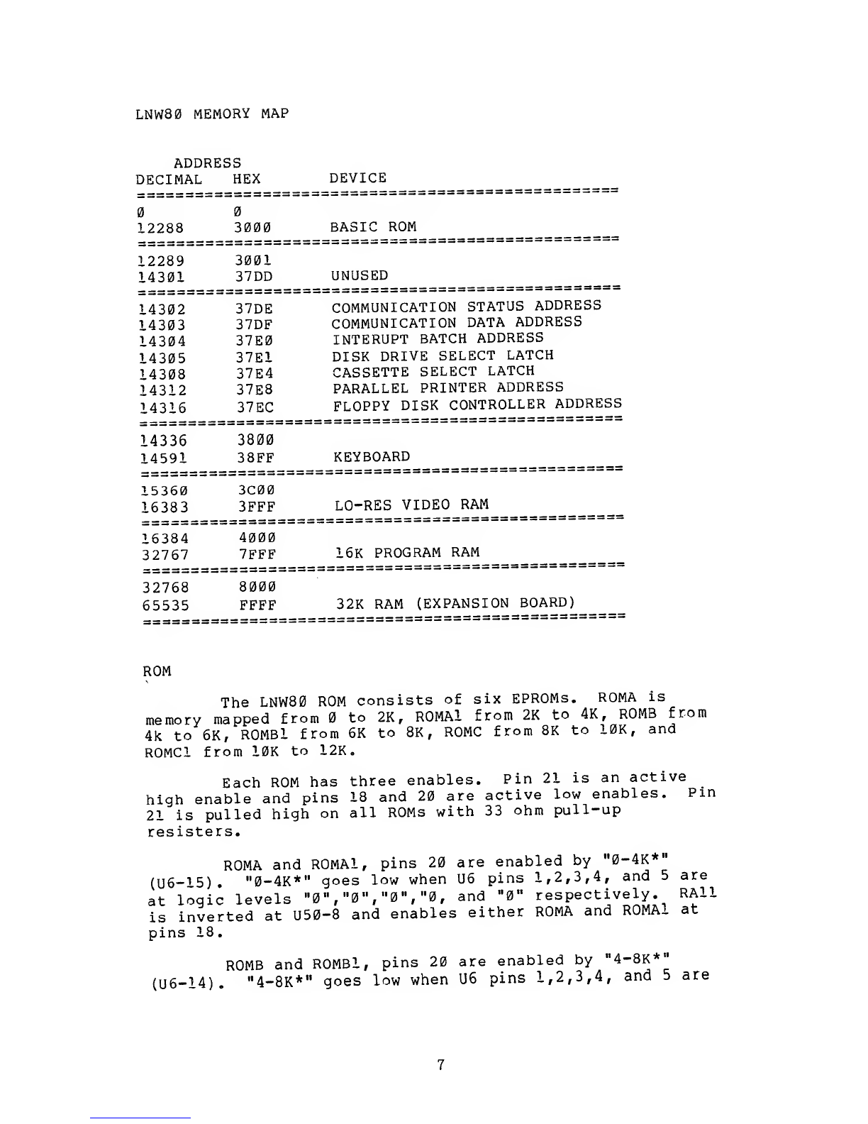
LNW80 MEMORY MAP
ADDRESS
DECIMAL HEX
12288 3000
========;======:
12289 3001
14301 37DD
===============:
14302 37DE
14303 37DF
14304 37E0
14305 37E1
14308 37E4
14312 37E8
14316 37EC
DEVICE
BASIC ROM
UNUSED
COMMUNICATION STATUS ADDRESS
COMMUNICATION DATA ADDRESS
INTERUPT BATCH ADDRESS
DISK DRIVE SELECT LATCH
CASSETTE SELECT LATCH
PARALLEL PRINTER ADDRESS
FLOPPY DISK CONTROLLER ADDRESS
14336 3800
14591 38FF KEYBOARD
15360 3C00
16383 3FFF LO-RES VIDEO RAM
16384 4000
32767 7FFF 16K PROGRAM RAM
32768 8000
65535 FFFF 32K RAM (EXPANSION BOARD)
ROM
The LNW80 ROM consists of six EPROMs. ROMA is
memory mapped from to 2K, ROMAl from 2K to 4K ,ROMB from
4k to 6K, R0MB1 from 6K to 8K, ROMC from 8K to 10K, and
ROMC1 from 10K to 12K.
Each ROM has three enables. Pin 21 is an active
high enable and pins 18 and 20 are active low enables. Pin
21 is pulled high on all ROMs with 33 ohm pull-up
resisters.
ROMA and ROMAl, pins 20 are enabled by "0-4K*"
(U6-15). "0-4K*" goes low when U6 pins 1,2,3,4, and 5are
at logic levels "0" ,"0" ,"0" ,"0 ,and "0" respectively. RAll
is inverted at U50-8 and enables either ROMA and ROMAl at
pins 18.
ROMB and ROMBl, pins 20 are enabled by "4-8K*"
(U6-14). "4-8K*" goes low when U6 pins 1,2,3,4, and 5are
at logic levels "1", "0", "0",
»
», and "0" respectively. RA11
enables either ROMB or R0MB1 at pins 18.
ROMC and R0MC1
(U6-13). "8-12K*"
at logic levels "0
enables ROMC or ROMC1 at
pins 20 are enabled by "8-12K*"
goes low when U6 pins 1,2,3,4, and 5are
"1","0","0\ and "0" respectively. RA11
pins 18.
and
and U65 Addresses
,LS244' A0 through All are buffered through U62
s. The data bus out is buffered through U63
by "RAM/ROM*" (U52-6). "RAM/ROM*" goes low
when RD* occurs with either "0-4K*", "4-8K*", or "8-12K*".
is enabled
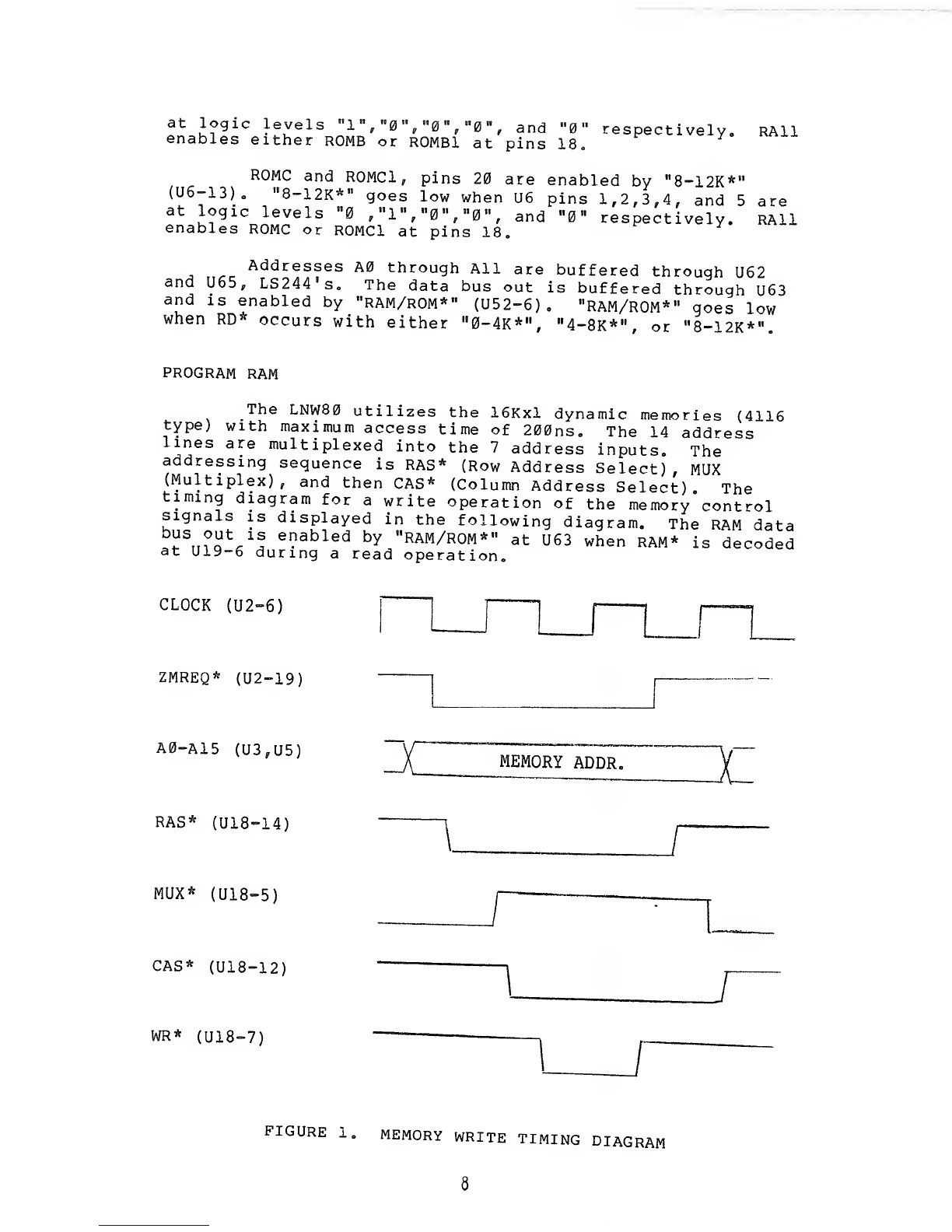
PROGRAM RAM
The LNW80 utilizes the 16Kxl dynamic memories (4116
type) with maximum access time of 200ns. The 14 address
lines are multiplexed into the 7address inputs. The
addressing sequence is RAS* (Row Address Select), MUX
(Multiplex), and then CAS* (Column Address Select). The
timing diagram for awrite operation of the memory control
signals is displayed in the following diagram. The RAM data
?ma Vf e?abled bV"RAM/ROM*" at U63 when RAM* is decoded
at U19-6 during aread operation.
CLOCK (U2-6)
ZMREQ* (U2-19)
A0-A15 (U3,U5)
RAS* (U18-14)
MUX* (U18-5)
CAS* (U18-12)
WR* (U18-7)
MEMORY ADDR.
J
FIGURE 1. MEMORY WRITE TIMING DIAG RAM

RAM REFRESH
Dynamic RAM require periodic refreshing to retain
data information. If the system does not receive periodic
refreshing the dynamic RAMs will begin to "forget" data.
The LNW80 utilizes the Z80A CPU to generate the
refresh to the RAM's. The memory refresh address is output
on the lower 7address bits during refresh time. An
instruction fetch will increment the refresh register.
The LNW80 uses a"RAS*" only refresh, where RAS*
will be low and CAS* will be high during refresh. At
refresh time MUX will be low selecting A0-A7 as the RAM
address.
KEYBOARD
The LNW80 keyboard is designed specifically for the
LNW80 computer providing a62 keypad, an 11 key numeric
keypad, and all the special functions that are available to
you through the LNW80 computer.
an
Note that lower case is enabled only with software
driver routines such as those available in DOS+, NEWDOS80,
and ELECTRIC PENCIL.
SPECIAL KEYBOARD FUNCTIONS
RESET (RST)
HIGH LOW:
CONTROL:
CAPS LOCK:
Fl, F2:
Both RST keys must be depressed to reset
the computer.
Forced LOW Speed switch. When depressed
the system will operate in LOW speed.
Otherwise the system will operate in
forced high speed.
This is aspecial software controlled key.
It is used in software such as the
ELECTRIC PENCIL word processing program.
Disables lower case characters.
User definable keys. Needs special
software driver.

VIDEO DIVIDER CHAIN
The video divider chain provides the necessary logic
for video processing, including video ram addressing, and
vertical and horizontal timing pulses. The basis of the
video divider chain is the 10.738MHz clock at U119-6. This
signal appears as asine wave and is exactly 3times the
color frequency of 3„579MHz. U121 executes adivide by 2.
This results in 2input frequencies to the divider chain at
U122.
In the standard 64 character mode, 32CHAR* (U122-1)
will be high so that the Binputs to U122 will be selected
therefore the clock input at U138-9, CLKT, will be
10.738MHz. U138 provides the basic timing signals for video
processing. Figure 2represents atiming diagram for the
outputs of U138 and U155 in the 64 character mode.
CLKT 11
(U138-9) 1~mjnj~Ln_n_n_r_ri
Ti 1
(U138-5) —
1
T2
(U138-7)
«!•)
1J
(U138-10)
T4
(U138-12)
T5
(U138-15)
T6
(U138-2)
T7
(U155-6)
FIGURE 2
10

During 64 character mode, T7* is selected as the
control clock (CNTRCLK) for the video timing chain (U122-12)
.
The circuitry of U138 and U155 effectively produces adivide
by 12 such that T7* is 10.738MHz/12 or 894.8KHz. Note also
that T7 is selected as CHARl (U122-9) .CNTRCLK is the clock
input to U160 and U161 (S161 's) .Figure 3illustrates the
outputs of U160 and U161.
T7 (U155-6)
894.88KHZ ji^juimnmuwLnjLam
CHAR2 (U161-14)
447.4KHZ
CHAR4 (U161-13)
223.7KHZ
CHAR8 (U161-12)
111.86KHZ
CHAR16 (U161-11)
55.93KHZ
CHAR32 (U160-14)
27.97KHZ
FIGURE3
Note that HORTP (U160-13) is not half the frequency
of CHAR32 (U160-14) .T6INH* (U155-9) prevents the completion
of its period by clearing U160 and U161 at the end of each
horizontal line. The frequency of HORTP is 15.750KHz
resulting in aperiod of 63.49us for each line.
Each line consists of 112 characters. Allowing one
CHARl period for each 2characters the time span for 112
characters is 62.58us. Note that we are left with 0.91us at
the end of each horizontal line. T6INH* is used to delay
the timing chain to "waste" this additional time before
starting the next cycle. U167 is used to add the additional
delay in T6INH*. It is ANDed with T6 at U154 thus delaying
T6*(U154-8) from clearing U138.
HSTP (U168-11) is the ORing of CHAR16 and CHAR32,
ANDed with HORTP. This is the horizontal sine timing pulse.
Its frequency is 15.750KHz. Refer to figure 4for the
timing diagram.
11

U159-12 is also displayed in figure 4, It goes low
after the 112th character and also has afrequency of
15.750KHz oIt serves 2important purposes. 1st, it is the
data input to U124 which when clocked clears U155 and thus
enabling T6INH*. Also it is the input to U156-13 and thus
increments the row count.64th Char Position 112th Char Position
f
CHAR16
(U161-11)
CHAR32
(U160-14)
HORTP
(U160-13)
HSTP
(U168-11)
"U159-12" T
FIGURE 4.
Each character position consists of a6x12 matrix.
Six dots and 12 horizontal rows. U156 increments by one
after each horizontal scan. When the row count is equal to
12, U168-3 will go high thus clearing U156 setting the row
count back to zero and also clocking U153-11 and
incrementing the line count by one.
Note that the screen consists of 22 lines (only 16
are displayed) and each line has 12 rows. LINEl, the least
signicicant bit of the line counter, changes state every 2nd
line and thus has the same period as 24 rows or 24x63. 49us
or 1.524ms. Its frequency is therefore 656.3Hz. Using
similar logic, you can find that LINE2=328.lHz,
LINE4=164.1Hz, and LINE8=82.0Hz.
Asimilar situation exists for VERTP (U156-6) as did
for HORTP in that U156 is cleared before VERTP, which
represents line!6, completes its full period. When the
total line count is 22 the inputs to U169 pins 3,4 and 5are
high, thus its output pin6 clears the line count back to
zero, in 22 lines LINEl changes state 11 times so that the
period of VERTP is 11 times that of LINEl or 16.76ms. The
resultant VERTP frequency is 59.66Hz.
In the 32 character mode, U122-1 goes low selecting
the 5.369MHz clock for CLKT. The result is that all of the
outputs of U138 are exactly one half the frequency that they
12
CTI co ro H» O§
(D 00 CD IP CO fO
si-1
CD CD
X
5*. XCD
M(-» *>
Wro II
ii CO
Wi-» GO
Bro
M*—*X
O<V»^
2^—
'
o
ro
CO B
M
o
2CO
M
o
s
CD
X
CD
ii
H» CD
ID XCD
ro *~*
<^r°s
o
5
o
t-3
W
H1
en
CD
—CO
£§
OCO
HH
WO
W2
o
CO
O
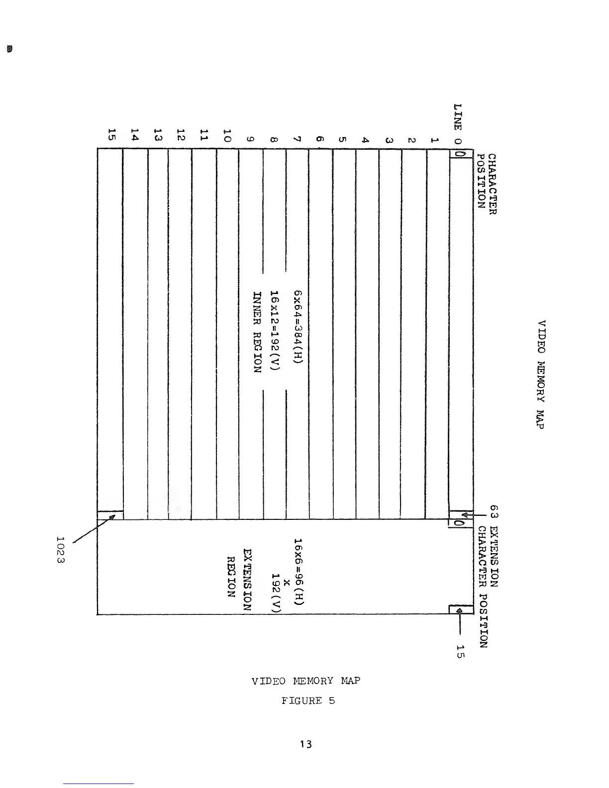
VIDEO MEMORY MAP
FIGURE 5
13
were in 64 character mode. T5* is selected as CNTRCLK and
CHAR1 is ground. Note that because T7* is 1/2 the frequency
of T5®, by selecting T5* in 32 character mode CNTRCLK does not
change and therefore nor does the resulting logic of U160 and
U161.
The signals that did change, T2 through T5 and CHAR1
,
are very important to the video processor section. CHAR1
determines whether the video ram have 1024 or512 usable
addresses. T2 through T5 determine how many characters may be
processed to the character generator per line.
VIDEO RAM ADDRESSING
The video rams are addressed by 2sources. The video
divider chain addresses the video ram so that data contained
in memory can be processed and displayed on the screen. The
CPU must address the video ram so that data can be read from
or writen to specific locations. Multiplexers are used to
select either the video chain or CPU address.
For the following discussion refer to figure 5, the
VIDEO MEMORY MAP. Note that the low resolution video is
defined only within the inner region and that A10-A13, which
specify the row count are not used by the low resolution video
ram. By definition A10-A13 are at alogic "1" voltage state
during CPU access of the low resolution video ram.
The inner region represents the standard TRS80* video
display. This region is memory mapped at locations 15360
through 16383. It has 63 characters and 16 lines, each line
with 12 rows. The video addressing of this region is
represented by the following:
384 X192 INNER REGION
ROW |LINE ICHARACTER
15 14 13 12 11 10 987654321(ADDRESS)
SPECIFIES
ROWS
0-11
SPECIFIES
LINES
0-15
SPECIFIES CHAR
POSITION
0-63
A0-A5 specify character position 0-63, A6-A9 specify
line position 0-15, and A10-A13 specify row position 0-11.
A14 and A15 will be low.
ie extension region, refer to figure 5
16 character positions for atotal of
The
additional
following illustrates the addressing" of this region:
adds an
80. The
14
96 X192 EXTENSION REGION
1 1 ROW LINE ROW CHAR
SPECIFIES
LEAST
SIGNIFICANT
2BITS OF 4
BIT ROW FIELD
15 14 13 12 11 10 987654 3 2 I(ADDRESS)
SPECIFIES 4BIT
FIELD WHICH
DEFINES THE
EXTENSION REGION
CHARACTER POSITION
SPECIFIES
LINES
0-15
SPECIFIES
MOST
SIGNIFICANT
2BITS OF 4
BIT ROW FIELD
A0-A3 specify character 0-15 of the extension
region, A4-A5 specify the most significant 2bits of the 4
bit row field, A6-A9 specify lines 0-15, and A10-A11 specify
the least significant 2bits of the 4bit row field. A12
and A13 are high. Note that the extension region is
uniquely defined by alogic"!" at A12 and A13 because in the
inner region this would specify arow count greater than
11.
When the CPU is not accessing the video ram, the
video addresses are controlled by the video divider chain.
The selects at U139, U140, U144, and U145 will be high
selecting the Binputs.
U142 specifies whether we are in the inner or
extension region. Prior to the 64th character HORTP (U142-1)
will be low, selecting the Ainputs. At the 64th character
HORTP will go high selecting the Binputs thus selecting the
extension region addresses.
CPUACC*(Ul21-8) is the select for U139, U140, U144,
and U145. When the CPU is accessing the video ram, CPUACC*
will go low selecting the Ainputs. The procedure by which
CPUACC* goes low and the CPU addresses are latched into the
address multiplexers will be covered in afollowing
section.
LOW RESOLUTION VIDEO RAM
Video Ram consists of two 2114
For either read or write
8) must be low. They have an
address lines, and 4data lines
each. U114 uses the least 4significant data bits and U115
the 4most significant data bits.
The Low-Resolution
type 1Kx4 static ram chips,
operations the select (pin
active low write enable, 10
15
Other manuals for LNW-80
1
Table of contents
Other LNW Research Desktop manuals


