LS RESEARCH TIWI-UB1 User manual

The information in this document is subject to change without notice.
330-0134-R1.0 Copyright © 2013 LS Research, LLC Page 1of 26
TIWI-UB1 EM BOARD
User Guide
Last updated
August 14th, 2013

TiWi-uB1 Module
EM BOARD USER GUIDE
The information in this document is subject to change without notice.
330-0134-R1.0 Copyright © 2013 LS Research, LLC Page 2of 26
Table of Contents
1Introduction...................................................................................................................3
1.1 Purpose & Scope.......................................................................................................................3
1.2 Applicable Documents ...............................................................................................................3
1.3 Revision History .........................................................................................................................3
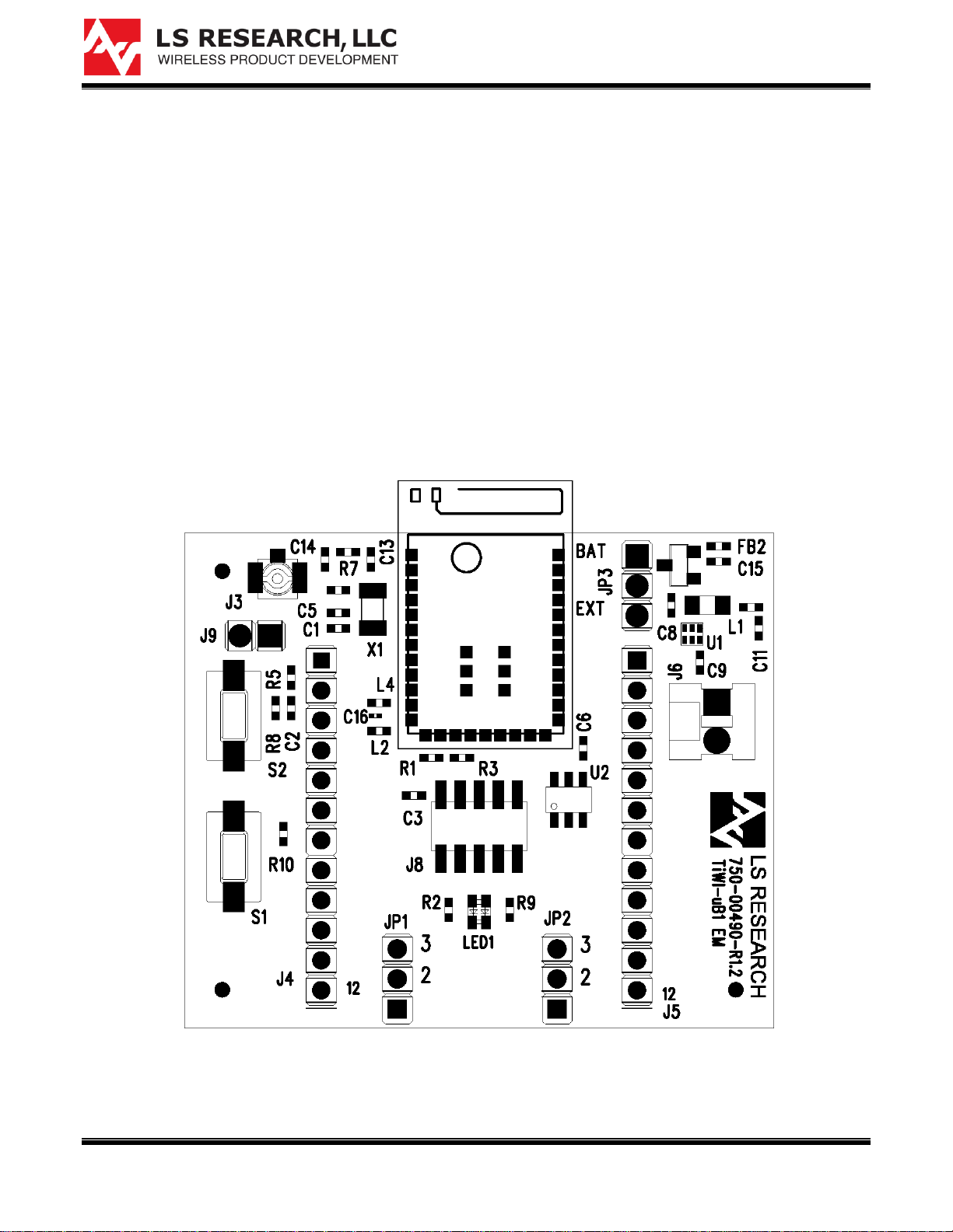
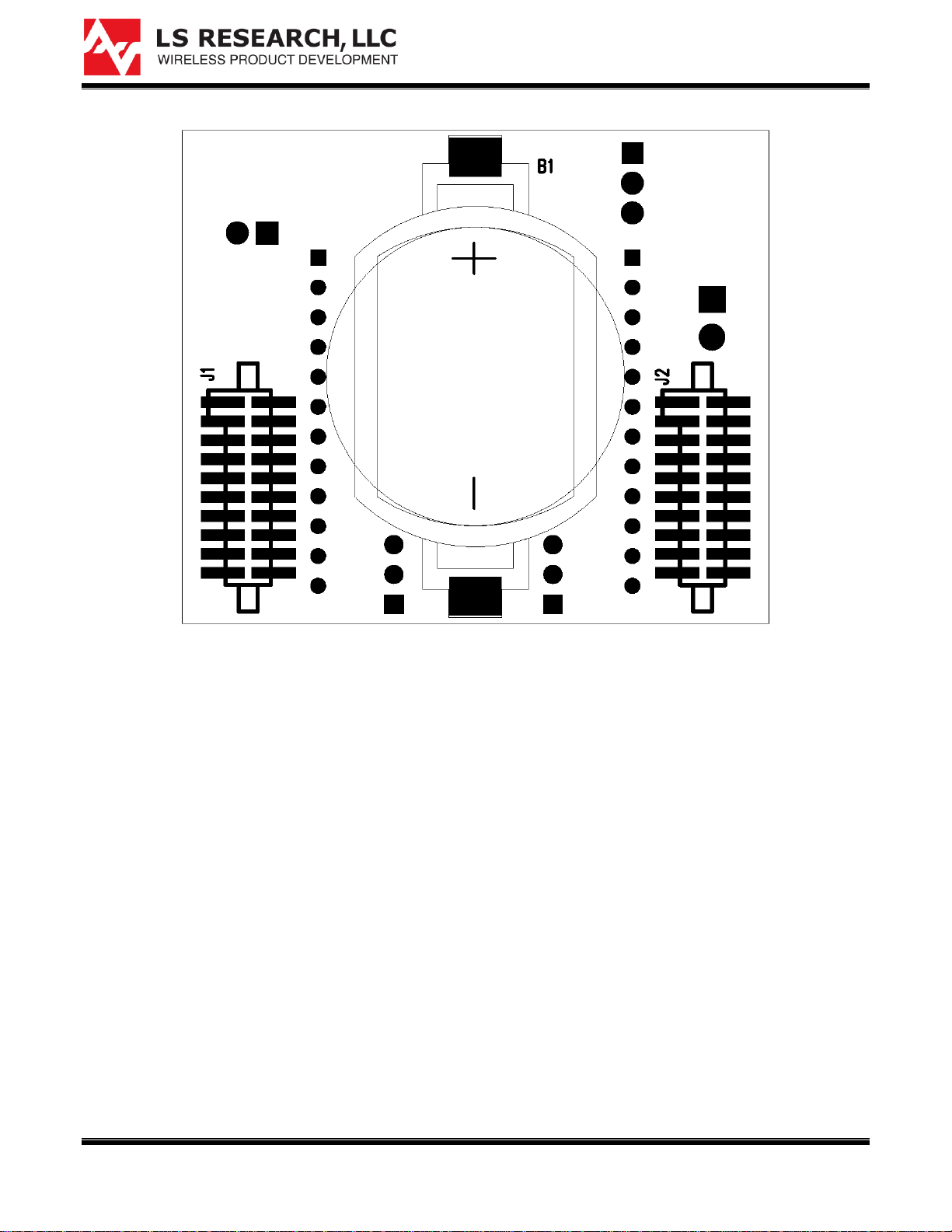
2TiWi-uB1 EM Board Description...................................................................................4
3TiWi-uB1 EM Board Hardware......................................................................................6
3.1 RF Connector.............................................................................................................................6
3.2 EM Interface Connectors ...........................................................................................................6
3.3 General Purpose Connectors ....................................................................................................9
3.4 Power Configuration Jumpers..................................................................................................11
3.5 LED Indicators..........................................................................................................................11
3.6 Push Button Switches..............................................................................................................11
3.7 Connecting EM Board to Host Platform...................................................................................12
3.8 I²C Interface .............................................................................................................................13
4TiWi-uB1 EM Board Schematic ..................................................................................14
4.1 Bill Of Material (BOM)..............................................................................................................15
5Application Development ...........................................................................................16
5.1 Overview ..................................................................................................................................16
5.2 Development Tools ..................................................................................................................16
5.3 Software Development.............................................................................................................25
6Contacting LS Research.............................................................................................26

TiWi-uB1 Module
EM BOARD USER GUIDE
The information in this document is subject to change without notice.
330-0134-R1.0 Copyright © 2013 LS Research, LLC Page 3of 26
1Introduction
1.1 Purpose & Scope
The purpose of this document is to provide details regarding the setup and use of
the TiWi-uB1 module on an EM board. This document covers a description of
the EM board and its features and a brief tutorial on how to operate the module
EM board.
1.2 Applicable Documents
TiWi-uB1 Datasheet (330-0132)
TiWi-uB1 Antenna Design Guide (330-0133)
1.3 Revision History
Date
ECN
Change Description
Revision
8/14/2013
87-2013
Initial release
1.0
Table 1 Revision History

TiWi-uB1 Module
EM BOARD USER GUIDE
The information in this document is subject to change without notice.
330-0134-R1.0 Copyright © 2013 LS Research, LLC Page 4of 26
2TiWi-uB1 EM Board Description
The TiWi-uB1 EM “Evaluation Module” Board is an evaluation platform for the LS Research TiWi-
uB1 Bluetooth Smart module. The TiWi-uB1 EM Board provides all of the necessary connectors,
jumpers, indicators and switches to test and debug all aspects of the TiWi-uB1 module. The EM
board is intended for evaluation purposes when used by itself or in conjunction with various Texas
Instruments development boards. When used by itself, an on board coin cell battery or external
power supply is used to power the TiWi-uB1 and its various peripherals.
The TiWi-uB1 EM board can be used to evaluate basic BLE connectivity. Additionally it is possible
to put the TiWi-uB1 module into static RF test modes so that RF performance can be evaluated.
Either a Texas Instruments CC Debugger or SmartRF05EB is required to be used in conjunction
with the EM board for programming and debugging. The CC Debugger and SmartRF05EB are not
provided by LSR and need to be purchased separately from Texas Instruments.
Figure 1 TiWi-uB1 EM Board Top Side

TiWi-uB1 Module
EM BOARD USER GUIDE
The information in this document is subject to change without notice.
330-0134-R1.0 Copyright © 2013 LS Research, LLC Page 5of 26
Figure 2 TiWi-uB1 EM Board Bottom

TiWi-uB1 Module
EM BOARD USER GUIDE
The information in this document is subject to change without notice.
330-0134-R1.0 Copyright © 2013 LS Research, LLC Page 6of 26
3TiWi-uB1 EM Board Hardware
3.1 RF Connector
There are two TiWi-uB1 Module versions:
LSR Part Number
Description
450-0103
TiWi-uB1 Module, PCB Trace Antenna
450-0106
TiWi-uB1 Module, RF Castellation (Onboard Antenna Disabled)
Table 2 Module Part Numbers
The TiWi-uB1 EM board includes an on board U.FL RF connector J3 (Figure 1). When used in
conjunction with TiWi-uB1 450-0106, J3 provides an RF connection point to external antennas
or test equipment. When the TiWi-uB1 EM board is used with used with TiWi-uB1 450-0103,
the U.FL connector has no electrical connection to the TiWi-uB1 450-0103.
The TiWi-uB1 is modular certified for FCC 15.247 and IC RSS-210, as well as compliant to the
RF requirements for ETSI EN 300 328 and ETSI EN 301 489. The TiWi-uB1 450-0106 has
modular certification when used with LSRs 001-0001 2.4 GHz Dipole Antenna with Reverse
Polarity SMA Connector.
See the TiWi-uB1 datasheet and antenna user’s guide for further information regarding FCC/IC
modular certification.
3.2 EM Interface Connectors
There are two primary connectors on the TiWi-uB1 EM Board, J1 & J2. These provide a
standard interface to Texas Instruments development platforms. Refer to Table 3 and Table 4
below for details on the signals brought out to the EM connectors J1 and J2.
1.2"
J1 J2
19
2
20
1
19
2
20
1
Figure 3 TiWi-uB1 EM Board Bottom

TiWi-uB1 Module
EM BOARD USER GUIDE
The information in this document is subject to change without notice.
330-0134-R1.0 Copyright © 2013 LS Research, LLC Page 7of 26
J1 Pin
Number
Pin Name
Module
Pin Type
Description
1
GND
Power
Ground
2
NC
Not Connected
3
P0.4
Digital I/O
Digital input/output
4
P1.3
Digital I/O
Digital input/output
5
P0.1
Digital I/O
Digital input/output
6
P1.0
Digital I/O
Digital input/output, 20mA output drive capable
7
P0.2
Digital I/O
Digital input/output
8
NC
Not Connected
9
P0.3
Digital I/O
Digital input/output
10
P2.1
Digital I/O
Debug Data or digital input/output
11
P0.0
Digital I/O
Digital input/output
12
P2.2
Digital I/O
Debug Clock or digital input/output
13
P1.1
Digital I/O
Digital input/output, 20mA output drive capable
14
P1.4
Digital I/O
Digital input/output
15
P0.6
Digital I/O
Digital input/output
16
P1.5
Digital I/O
Digital input/output
17
P0.7
Digital I/O
Digital input/output
18
P1.6
Digital I/O
Digital input/output
19
GND
Power
Ground
20
P1.7
Digital I/O
Digital input/output
Table 3 EM Connector J1

TiWi-uB1 Module
EM BOARD USER GUIDE
The information in this document is subject to change without notice.
330-0134-R1.0 Copyright © 2013 LS Research, LLC Page 8of 26
J2 Pin
Number
Pin Name
Module
Pin Type
Description
1
NC
Not Connected
2
GND
Power
Ground
3
NC
Not Connected
4
NC
Not Connected
5
NC
Not Connected
6
NC
Not Connected
7
VIN
Power
Power supply input (2.0v to 3.6v)
8
NC
Not Connected
9
VIN
Power
Power supply input (2.0v to 3.6v)
10
NC
Not Connected
11
NC
Not Connected
12
SCL
Digital I/O
I2C clock or digital input/output
13
NC
14
SDA
Digital I/O
I2C data or digital input/output
15
/RESET
Digital Input
Active low reset to module
16
NC
Not Connected
17
P1.2
Digital I/O
Digital input/output
18
P0.5
Digital I/O
Digital input/output
19
P2.0
Digital I/O
Digital input/output
20
NC
Not Connected
Table 4 EM Connector J2

TiWi-uB1 Module
EM BOARD USER GUIDE
The information in this document is subject to change without notice.
330-0134-R1.0 Copyright © 2013 LS Research, LLC Page 9of 26
3.3 General Purpose Connectors
3.3.1 J6 Power Supply Input
J6 Pin
Number
Pin Name
Module
Pin Type
Description
1
VIN
Power
Power supply input (2.0v to 3.6v)
2
GND
Power
Ground
Table 5 Power Connector J6
3.3.2 J4 & J5 External Interface Headers
J4 Pin
Number
Pin Name
Module
Pin Type
Description
1
/RESET
Digital Input
Active low reset to module
2
P2.2
Digital I/O
Debug Clock or digital input/output
3
P2.1
Digital I/O
Debug Data or digital input/output
4
P2.0
Digital I/O
Digital input/output
5
SCL
Digital I/O
I2C clock
6
SDA
Digital I/O
I2C data
7
P1.7
Digital I/O
Digital input/output
8
P1.6
Digital I/O
Digital input/output
9
P1.5
Digital I/O
Digital input/output
10
P1.4
Digital I/O
Digital input/output
11
P1.3
Digital I/O
Digital input/output
12
GND
Power
Ground
Table 6 Single Row Header J4
J5 Pin
Number
Pin Name
Module
Pin Type
Description
1
P0.7
Digital I/O
Digital input/output
2
P1.0
Digital I/O
Digital input/output, 20mA output drive capable
3
P1.1
Digital I/O
Digital input/output, 20mA output drive capable
4
P0.6
Digital I/O
Digital input/output
5
P0.5
Digital I/O
Digital input/output
6
VIN
Power Input
Power supply input (2.0v to 3.6v)
7
P0.4
Digital I/O
Digital input/output
8
P0.3
Digital I/O
Digital input/output
9
P0.2
Digital I/O
Digital input/output
10
P0.1
Digital I/O
Digital input/output
11
P0.0
Digital I/O
Digital input/output
12
P1.2
Digital I/O
Digital input/output
Table 7 Single Row Header J5

TiWi-uB1 Module
EM BOARD USER GUIDE
The information in this document is subject to change without notice.
330-0134-R1.0 Copyright © 2013 LS Research, LLC Page 10 of 26
3.3.3 J9 External 32kHz Clock Input
J9 Pin
Number
Pin Name
Module
Pin Type
Description
1
CLK_IN¹
Digital Input
Clock Input
2
GND
Power
Ground
1. Coupling capacitor C1 must be populated to use the external 32kHz clock input.
Table 8 External 32kHz Header J9
3.3.4 J8 Programming Header
J8 is the Texas Instruments CC Debugger interface to the TiWi-uB1 Module. The debug
interface implements a proprietary two-wire serial interface that is used for in-circuit debugging
and programming.
J8 Pin
Number
Pin Name
Module
Pin Type
Description
1
GND
Power
Ground
2
VIN
Power
Power Input
3
DBG_CLK
Digital Input
Debug Clock
4
DBG_DAT
Digital I/O
Debug Data
5
NC
Not Connected
6
NC
Not Connected
7
/RESET
Digital Input
Active low reset to module
8
NC
Not Connected
9
NC
Not Connected
10
NC
Not Connected
Table 9 Programming/Debug Header J8

TiWi-uB1 Module
EM BOARD USER GUIDE
The information in this document is subject to change without notice.
330-0134-R1.0 Copyright © 2013 LS Research, LLC Page 11 of 26
3.4 Power Configuration Jumpers
Jumpers JP1, JP2, and JP3 are used to select the various modes of powering the TiWi-uB1 EM
board.
JP1 and JP2 are used for test purposes only and should remain in positions 2-3.
JP3 is used to select either battery power or external power.
A TI TPS62730 (U1), 2.1V DC to DC converter is supplied, which when used with the TiWi-uB1
module, enables reduced peak and average current consumption up to 30% or more during
radio transmit or receive modes. This is especially important in battery-powered applications by
reducing current consumption while maintaining superior RF performance. See Current
Savings Using TPS62530 for more info.
1. Voltage on any digital pin to the TiWi-uB1 shall not exceed Max DVCC + 0.3V ≤ 3.9V or Min -0.3V.
2. When the TPS62730 bypass pin is asserted low, the TPS62730 is bypassed and AVCC/DVCC = VIN
Caution: Care must be taken when interfacing a battery powered TiWi-uB1 module to an externally powered Host
or other external input. If the host is providing input to the module at 3.0V while the module is powered at 2.1V,
the external input to the module will exceed DVCC + 0.3V requirement for the I/O and the TiWi-uB1 module will
be damaged.
3.5 LED Indicators
There are 2 LEDs on the TiWi-uB1 EM board:
LED1A - User Defined (connected to digital input/output P1.0, 20mA capable)
LED1B - User Defined (connected to digital input/output P1.1, 20mA capable)
3.6 Push Button Switches
There are two push button switches on the TiWi-uB1 EM board:
S1 - User defined switch
S2 - Manual reset to the module

TiWi-uB1 Module
EM BOARD USER GUIDE
The information in this document is subject to change without notice.
330-0134-R1.0 Copyright © 2013 LS Research, LLC Page 12 of 26
3.7 Connecting EM Board to Host Platform
The TiWI-uB1 can be operated in one of two different modes, determined by the firmware
programmed into the module:
Stand Alone Mode - This is the most common configuration when using the TiWi-uB1 Module.
In this mode, the controller, host, profiles, and application are all implemented on the TiWi-uB1
module as a true stand alone Bluetooth BLE solution. No interface to a host is required.
Network Processor Mode - The controller and host are implemented together on the TiWi-uB1
module, while the profiles and application are implemented separately. The application and
profiles communicate with the TiWi-uB1module by means of HCI commands using a SPI or
UART interface. This configuration is useful for applications which execute on either another
device (such as an external microcontroller) or a PC. In these cases, the application can be
developed externally while still running the BLE stack on the CC2540/41.
The TiWi-uB1EM board uses USART 0 as the default UART interface and USART 1 as the
default SPI interface (Figure 4).
Figure 4 TiWi-uB1 EM Board Interface to Host

TiWi-uB1 Module
EM BOARD USER GUIDE
The information in this document is subject to change without notice.
330-0134-R1.0 Copyright © 2013 LS Research, LLC Page 13 of 26
3.8 I²C Interface
The TiWi-uB1 EM board includes an I²C interface. The I²C provides an interface between the
TiWi-uB1 module and the on board temperature sensor (U2), as well as other I²C compatible
devices connected by the two-wire I²C serial bus. External components attached to the I²C bus
serially transmit and/or receive serial data to/from the I²C on the TiWi-uB1 module through the
two-wire I²C interface. The I²C bus supports any slave or master I²C -compatible device.
Figure 5 shows an example of an I²C bus. Each I²C device is recognized by a unique address
and can operate as either a transmitter or a receiver. A device connected to the I²C bus can be
considered as the master or the slave when performing data transfers. A master initiates a
data transfer and generates the clock signal, SCL. Any device addressed by a master is
considered a slave. I²C data is communicated using the serial data (SDA) pin and the serial
clock (SCL) pin.
Figure 5 I²C InterfaceTiWi-uB1 EM Board Schematic

TiWi-uB1 Module
EM BOARD USER GUIDE
The information in this document is subject to change without notice.
330-0134-R1.0 Copyright © 2013 LS Research, LLC Page 14 of 26
4TiWi-uB1 EM Board Schematic
Figure 6 TiWi-uB1 EM Board Schematics

TiWi-uB1 Module
EM BOARD USER GUIDE
The information in this document is subject to change without notice.
330-0134-R1.0 Copyright © 2013 LS Research, LLC Page 15 of 26
4.1 Bill Of Material (BOM)
Reference
Pop Opt
Part Number
Description
B1
BU2032SM-G
Connector, Battery, Vertical SMT, 2032, NA, NA, 20mm battery
C1
NP
GRM155R71C104KA88#
Capacitor, MLCC, 16V, 0402, X7R, 100nF
C13 C14
NP
C16
NP
250R05L2R4BV4T
Capacitor, MLCC, 25V, 0201, NPO, 2.4pF
C2
GRM1555C1H101JA01#
Capacitor, MLCC, 50V, 0402, COG, 100pF
C3 C6
GRM155R71C104KA88#
Capacitor, MLCC, 16V, 0402, X7R, 100nF
C5 C7
GRM1555C1H120JA01#
Capacitor, MLCC, 50V, 0402, COG, 12pF
C8 C9 C11 C15
C0402C225M9PAC#
Capacitor, MLCC, 6.3V, 0402, X5R, 2.2uF
FB1 FB2
BLM15HG102SN1#
Ferrite Bead, 0402, 1K Ohm @ 100MHz, 250mA
J1 J2
SFM-110-02-L-D-A
Connector, Header Female, Vertical SMT, Keyd, 2 x 10, 1.27mm,
Gold Finish
J3
U.FL-R-SMT-1#
Connector, U.FL Jack, Vertical SMT, DC to 6 GHz, NA, NA, Gold
Plated Contact
J4 J5
NRPN121PAEN-RC
Connector, Header Male, Vertical TH, Unshrouded, 1 x 12, 2mm,
Gold Finish
J6
640456-2
Connector, Header Male, Vertical TH, Unshrouded, 1 x 2, 100mil,
Tin Finish
J8
GRPB052VWQS-RC
Connector, Header Male, Vertical SMT, Unshrouded, 2 x 5, 50mil,
Gold Finish
J9
NP
PRPN021PAEN-RC
Connector, Header Male, Vertical TH, Unshrouded, 1 x 2, 2mm,
Gold Finish
JMP1 JMP2
JMP3
SPN02SXCN-RC
Connector, Shorting Jumper, Vertical TH, Black, 1 x 2, 2mm, Gold
Finish
JP1 JP2 JP3
NRPN031PAEN-RC
Connector, Header Male, Vertical TH, Unshrouded, 1 x 3, 2mm,
Gold Finish
L1
LQM21PN2R2NGC#
Inductor, Air Core Multilayer, 0805, 2.2uH
L2 L4
L-07C5N6SV6T
Inductor, Ceramic Core Multilayer, 0402, 5.6nH
LED1
APTB1612ESGC-F01
LED, Red/Green, 20mA, 2.0V, 12mcd, 0605, 625nm/568nm, Dual
Color SMT
MOD1
450-0106C
TiWi-uB1 Module, RF Castellation, CT
Q4
FDN340P
PCB, TiWi-uB1 EM Board
R1 R3
RK73B1ET#103J
Transistor, MOSFET, P-CHANNEL, SOT-23-3
R2 R9
CRCW0402270RFK#
Resistor, Thick Film, 0402, 10K
R5 R10
CRCW04022K70FK#
Resistor, Thick Film, 0402, 270
R7
RK73Z1ET#
Resistor, Thick Film, 0402, 2.7K
R8
NP
RK73B1ET#103J
Resistor, Thick Film, 0402, 0
S1 S2
EVQ-PNF04M
Resistor, Thick Film, 0402, 10K
U1
TPS62730DRY#
Switch, Tactile, SPST-NO, 50mA @ 12V, SMT
U2
TMP100NA#
IC, Switching Voltage Regulator, SON, Step Down Converter with
Bypass Mode
X1
ECS-.327-12.5-34B
IC, Temp Sensor, SOT-23-6, IIC
Table 10 TiWi-uB1 EM Board BOM

TiWi-uB1 Module
EM BOARD USER GUIDE
The information in this document is subject to change without notice.
330-0134-R1.0 Copyright © 2013 LS Research, LLC Page 16 of 26
5Application Development
5.1 Overview
The TiWi-uB1 EM Board has been designed to work either as a standalone development
platform or to be used in combination with one of TI various development platforms. This
flexible design platform allows the user to take advantage of the sample applications provided
by LSR as well as those provided by TI for the CC2541 SOC.
LSR’s Design Services team can be contracted to assist customers with application-specific
software or hardware development for TiWi-uB1 applications.
For an overview of development platforms and software examples see LSR Wireless Products
or TI CC2541 Bluetooth.
5.2 Development Tools
5.2.1 LSR TiWi-uB1 EM Board Stand Alone Application
The LSR development kit demonstrates the stand alone capability of the TiWi-uB1 EM
development board and connectivity to a Bluetooth® BLE enabled smartphone device. It
provides a platform to show the capability of Bluetooth® BLE for simple remote control of
devices and low data rate remote data collection and reporting.
LSRs TiWi-uB1 development kit hardware, sample firmware and iPhone Application allow the
user to:
Monitor temperature of the onboard temperature sensor U2
Monitor battery voltage
Monitor RSSI of data transmission from the TiWi-uB1 module to the iPhone
Monitor the status of the onboard pushbutton switch S1
Toggle the user defined LEDs 1A and 1B on and off
Track RF statistics such as number of BLE packets sent and received
Hardware required for the LSR Standalone evaluation application includes:
TiWi-uB1 EM Board with coin cell battery (Figure 7)
Figure 7 TiWi-uB1 EM BoardTI CC Debugger (Figure 8)
Bluetooth® 4.0 enabled iOS devices such as iPhone 4s or later, iPod Touch with LSR
application running (Figure 9)

TiWi-uB1 Module
EM BOARD USER GUIDE
The information in this document is subject to change without notice.
330-0134-R1.0 Copyright © 2013 LS Research, LLC Page 17 of 26
Figure 7 TiWi-uB1 EM Board
5.2.2 TI CC Debugger
The TI CC Debugger is used to program firmware into the TiWI-uB1 module. It can also be
used along with IAR Embedded Workbench for 8051 to write and debug custom firmware for
the TiWi-uB1 module. See TI CC Debugger for more information.
Figure 8 TI CC Debugger

TiWi-uB1 Module
EM BOARD USER GUIDE
The information in this document is subject to change without notice.
330-0134-R1.0 Copyright © 2013 LS Research, LLC Page 18 of 26
5.2.3 TiWi-uB1 EM Board Firmware
The TiWi-uB1 EM Board firmware can be downloaded from the TiWi-uB1 Wiki in binary or
source code form.
EM Board (BLE peripheral) Firmware Features
At startup the TiWi-uB1 module will start advertising and continue to advertise for ≈30
seconds. During advertising the red LED will be on.
Advertising can be turned on or off by pressing the USER (S1) button.
Once connected to a Central Device, the red LED will turn off. The connection interval is set
to 250ms.
Once connected, the USER button can be held for ≥8 seconds (hold until the red LED turns
on) to disconnect from the Central Device. After disconnecting the module will start
advertising right away.
Once connected, the user button can be held for ≥ 4 seconds (until the green LED turns on)
but not longer than 8 seconds to enable the TPS62730 regulator during battery voltage
readings. By default the battery voltage readings are done the TPS62730 in bypass mode
so the actual battery voltage can be read.
Four demo services are available in the firmware. Battery level, GPIO, range test, and
temperature.
5.2.4 iOS Application
The sample LSR iOS application can be used on any Apple device running iOS 5
or later. It is intended to demonstrate the capabilities of the TiWi-uB1 and
provides a starting point for users intending to write their own iOS applications.
The LSR iOS demonstration application performs the following functions:
Establishes a connection to any LSR TiWi-uB1 EM Board (Figure 10).
Displays RSSI (Received Signal Strength) of the iOS device and the LSR
TiWi-uB1 EM Board (Figure 11).
Allows the user to remotely control the LSR TiWi-uB1 EM Board LEDs
remotely (Figure 11).
Graphically shows the status of the LSR TiWi-uB1 EM Board on board user
switch (Figure 11).
Displays the temperature from the temperature sensor on board the LSR
TiWi-uB1 EM Board (Figure 11).
Displays the Battery or supply voltage of the LSR TiWi-uB1 EM Board (Figure
11).
Displays the RF statistics of the LSR TiWi-uB1 EM Board (Figure 12).

TiWi-uB1 Module
EM BOARD USER GUIDE
The information in this document is subject to change without notice.
330-0134-R1.0 Copyright © 2013 LS Research, LLC Page 19 of 26
Using the Demo iOS Application
Power up the TiWi-uB1 EM board using either a battery or an external power supply.
Start the LSR iOS application (Figure 9).
Touch the “Scan” button to scan for available TiWi-uB1 EM Boards. All available TiWi-uB1
devices within range will be displayed. (Figure 10).
Select the LSR TiWI-uB1 device to connect to (Figure 10).
Touch the “Connect to uB1 Module” button (Figure 10).
Once a connection to TiWi-uB1 EM board has been established with the iOS device, the red
LED on the TiWi-uB1 EM board will turn off and the “Control and Monitoring”screen will
become visible (Figure 11).
Slide the LED 1 and LED 2 slide switches to manually turn on and off the red and green
LEDs on the TiWi-uB1 EM board.
Momentarily press the user button on the TiWi-uB1 EM board and observe the Button Status
display box change from Released to Pressed.
Battery or Power supply voltage is displayed in the Voltage text box. Pressing the user
button for ≈ 5 sec will illuminate the Green LED, enable the 2.1 V regulator and the Voltage
text box should change to ≈ 2.1V. Pressing the user button again for ≈ 5 Sec will disable the
2.1V regulator and the real battery voltage will be read. Battery voltage updates every 5
seconds.
Touch the “RF Statistics” button at the bottom of the control and monitoring screen and the
“RF Statistics” screen will become visible showing RF statistics of the Bluetooth link between
the iOS device and the TiWi-uB1 EM board (Figure 11).

TiWi-uB1 Module
EM BOARD USER GUIDE
The information in this document is subject to change without notice.
330-0134-R1.0 Copyright © 2013 LS Research, LLC Page 20 of 26
Figure 9 Sample LSR iPhone Application
Table of contents