Table of Contents
Chapter1 INTRODUCTION
1.1 Preface
...............................................................................……….. 1-1
1.2 Key Features
......................................................................………. 1-1
1.3 Mainboard Layout
..............................................................………. 1-3
Chapter 2 HARDWARE INSTALLATION
2.1 Unpacking
................................................................................. 2-1
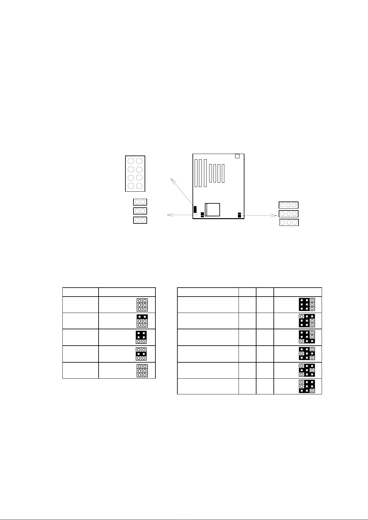
2.2 Jumper Setting Summary
....................................................... 2-2
2.3 CPUIstallation
.......................................................................... 2-4
2.3.1 CPU Frequency Configuration .................................... 2-4
2.3.2 CPU Voltage Configuration .......................................... 2-5
2.3.3 CPU Speed & Jumper Setting ..................................... 2-6
2.3.4 CPU Type Select Quick Reference .............................. 2-8
2.3.5 Installing a CPU in the ZIF Socket ............................... 2-16
2.4 Upgrading System Memory ..................................................... 2-17
2.4.1 Installing a SIMM Module............................................. 2-17
2.4.2 Installing a DIMM Module............................................. 2-18
2.4.3 DIMM Voltage Select ..................................….............. 2-18
2.4.4 Memory Module Installing Table .................................. 2-19
2.5 CMOS Clear Jumper.
............................................................... 2-20
2.6 FlashEPROMSelector
............................................................. 2-21
2.7 Connectors
............................................................................... 2-22
2.7.1 I/O Ports ....................................................................... 2-23
2.7.2 External Connections ................................................... 2-24
Chapter 3 BIOS Setup Program
3.1 StandardCMOSSetup
............................................................ 3-2
3.2 BIOSFeaturesSetup
.............................................................. 3-3
3.3 Chipset Features Setup
.......................................................... 3-6
3.4 Power Management Setup
...................................................... 3-12
3.5 PNP/PCIConfiguration
............................................................ 3-18
3.6 Integrated Peripherals.............................................................. 3-21
3.7 LoadSetupDefaults
................................................................ 3-25
3.8 PasswordSetting
.................................................................... 3-25
3.9 IDEHDDAutoDetection
.......................................................... 3-26