M-TI R558 User manual

PENTIUM PCI/IS
A
ATX Form PCI & ISA Bus Pentium Mainboard
On Board PCI Master IDE, Multi-I/O, VGA.
_________________________________________________________________
Users Manual
※※※※※※※※※※※※※※※※※※※※※※※※※※※※※※※※※※※※

_________________________________________________________________
Introduction
Welcome to the M-Technology next generation high performance
Pentium system mainboard --- R-558. The R-558 using the high
performance SIS 5598/5582 Chipset that will deliver superior
performance on your personal computer.
About This User's Guide
This User's Guide is for assisting system manufacturers and end users
in setting up and installing the mainboard. Information in this guide has
been carefully checked for reliability; however, there may
still be inaccuracies and information in this document is subject to
change without notice.
DISCLAIMER
The information in this manual has been carefully checked and is
believed to be accurate. We assumes no responsibility for any
inaccuracies that may still be contained in this manual. We reserves
the right to make changes to this material at any time without notice.
※All Brand names are trademarks of their owners.
____________________________________________________________________
*Our home page on Internet "http: //www.mtiusa.com"

Table of Contents
Chapter 1 INTRODUCTION
1.1 Preface ................................................................................. 1-1
1.2 Key Features ........................................................................ 1-1
1.3 Mainboard Layout ................................................................ 1-3
Chapter 2 HARDWARE INSTALLATION
2.1 Unpacking ................................................................................ 2-1
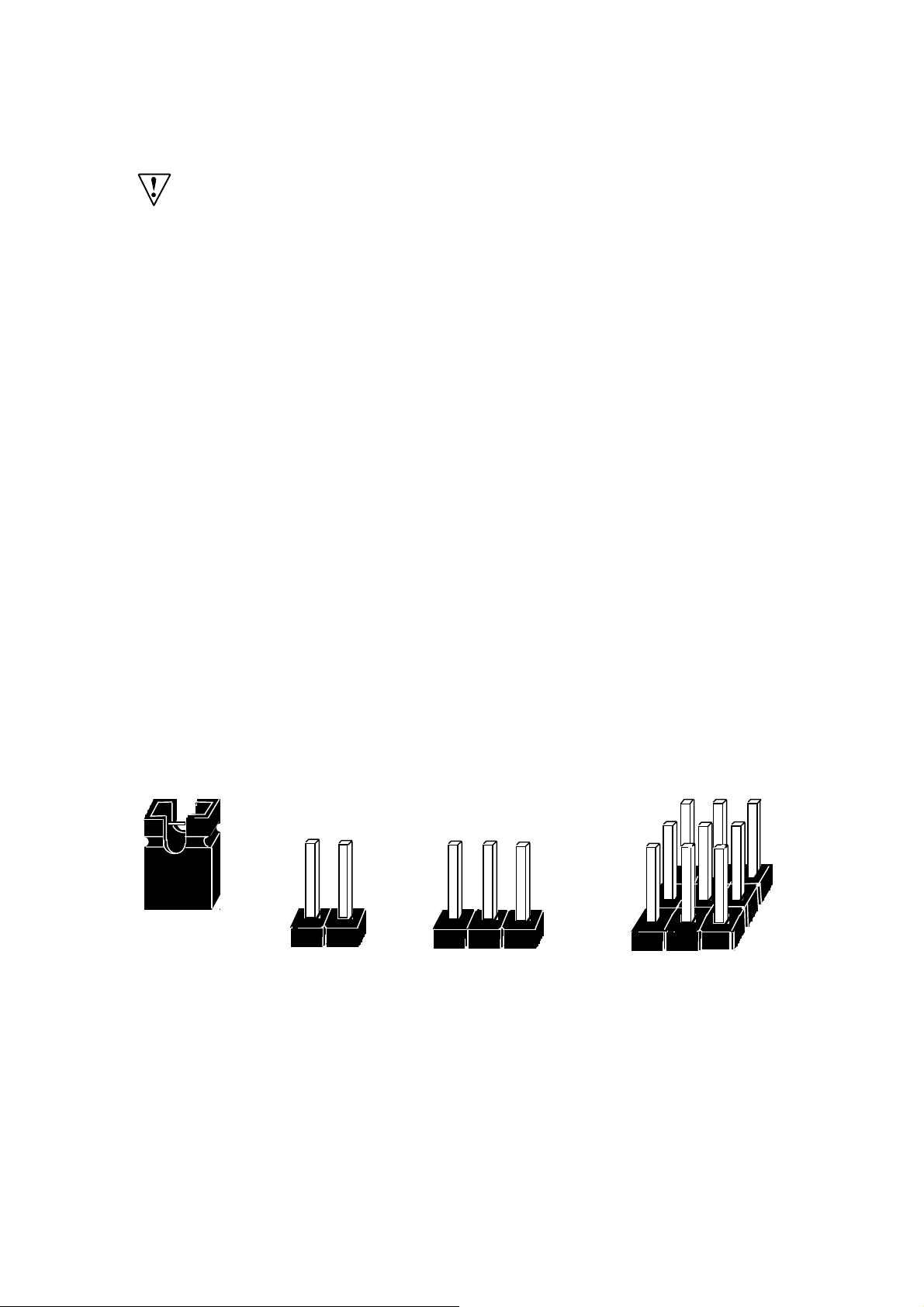
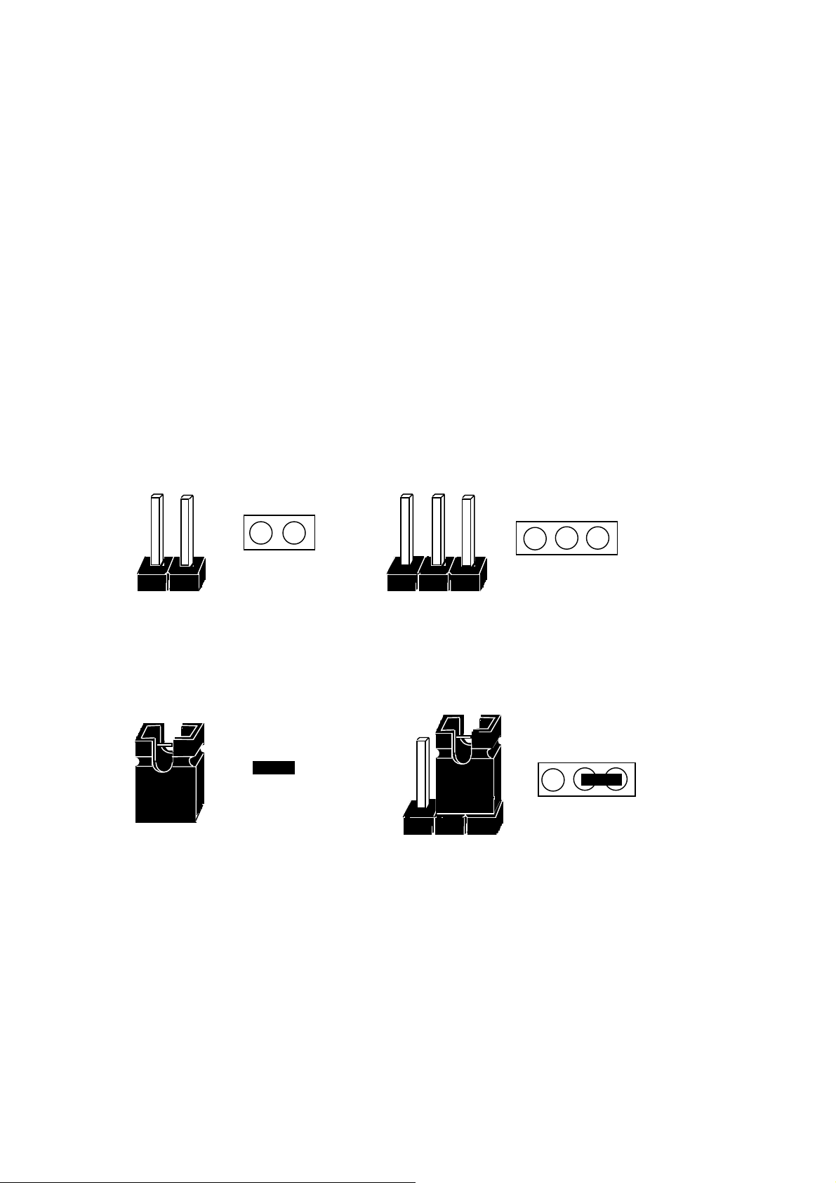
2.2 Jumper Setting Summary ..................................................... 2-2
2.3 CPU Istallation ......................................................................... 2-4
2.3.1 CPU Frequency Configuration ...................................... 2-4
2.3.2 CPU Voltage Configuration ........................................... 2-5
2.3.3 CPU Speed & Jumper Setting ....................................... 2-6
2.3.4 CPU Type Select Quick Reference ............................... 2-8
2.3.5 Installing a CPU in the ZIF Socket ................................. 2-16
2.4 Upgrading System Memory .................................................. 2-17
2.4.1 Installing a SIMM Module................................................ 2-17
2.4.2 Installing a DIMM Module................................................ 2-18
2.4.3 DIMM Voltage Select ..................................................... 2-18
2.4.4 Memory Module Installing Table .................................... 2-19
2.5 CMOS Clear Jumper. ............................................................. 2-20
2.6 Flash EPROM Selector .......................................................... 2-21
2.7 On Board VGA Optional.......................................................... 2-22
2.8 Connectors ............................................................................... 2-23
2.8.1 I/O Ports ........................................................................... 2-24
2.8.2 External Connections ...................................................... 2-25
Chapter 3 Award BIOS Setup Program
3.1 Standard CMOS Setup ............................................................ 3-2
3.2 BIOS Features Setup ............................................................ 3-4
3.3 Chipset Features Setup ......................................................... 3-6
3.4 Power Management Setup ...................................................... 3-9
3.5 PNP/PCI Configuration ............................................................ 3-12
3.6 Load Setup Defaults ................................................................ 3-14
3.7 Integrated Peripherals ............................................................ 3-14
3.8 Supervisor Password & User Password Setting ................. 3-16
3.9 IDE HDD Auto Detection ......................................................... 3-17
3.10 Save and Exit Setup ................................................................ 3-18
3.11 Exit Without Saving ................................................................. 3-18

Chapter 4 About the ATX Power Supply 4-1
Chapter 5 IDE Drivers
5.1 Introduction .............................................................................. 5-1
5.2 SIS IDE Driver Installation for DOS ........................................ 5-1
5.3 SIS IDE Driver Installation for Windows 3.x .......................... 5-2
5.4 SIS IDE Driver Installation for Windows 95............................ 5-3
5.5 SIS IDE Driver Installation for Windows NT 3.5x .................. 5-3
5.6 SIS IDE Driver Installation for Windows NT 4.0 .................... 5-4
5.7 SIS IDE Driver Installation for OS/2 ........................................ 5-5
5.8 Q & A ........................................................................................ 5-5
Chapter 6 VGA Drivers
6.1 Introduction .............................................................................. 6-1
6.2 DOS Utility ................................................................................ 6-2
6.3 ET24(CHINESE)....................................................................... 6-7
6.4 Windows NT 3.5 & 3.51.......................................................... 6-8
6.5 Windows NT 4.0....................................................................... 6-9
6.6 Windows 95 ............................................................................. 6-10
6.7 Windows 3.1............................................................................. 6-11
6.8 IBM OS/2 Warp 3.0(Double Byte Charactor).................... 6-14
6.9 IBM OS/2 Warp 3.0(Single Byte Charactor)...................... 6-15
6.10 Video Modes............................................................................ 6-17
Chapter 7 Q & A 7-1

_________________________________【
【【
【1】
】】
】
1. INTRODUCTION
1.1. Preface
Welcome to use the R-558 Pentium system mainboard. This manual
explains how to use this mainboard and install upgrades. It has
overview of the design and features of the board and provides useful
information on the configuration of the board, or a system in which.
1.2. Key Features
The R-558 Pentium system mainboard is a high-performance system
board that support Intel Pentium family CPUs, Cyrix, AMD and other
compatible CPUs.
There has many performance and system features integrated onto the
mainboard, including the following :
CPU : Supports Socket 7 for
- Intel Pentium 90 to 233 MHz, P55C (MMX).
- Cyrix / IBM 6x86, 6x86L, 6x86MX (M2),
- AMD K5, K6 .
and other compatible CPUs.
Chipset : SiS 5598/5582
Supports true 64 bits CACHE and DRAM access mode.
Supports 512K Pipelined Burst SRAM in second Level Cache.
CPU L1/L2 Write-Back Cache operation.
Supports 4x72-pin SIMM Sockets and 2 x 168-pin DIMM SDRAM or DRAM
Sockets.
- The Memory Capacity from 4MB to 384MB.
- Supports FP(Fast Page), EDO(Extended Data Out) Mode DRAM
and SDRAM.
Four 16-bit ISA Slots and Four 32-bit PCI Master Mode Slots.
______________________________________________________________
1-1

【
【【
【1】
】】
】__________________________________
Embeded 64-bit SVGA Chip (optional, SiS 5598 Chipset only)
- High performance 64-bit GUI accelerator with excellent video playback
capability
- System memory shares up to 4MB with video buffer
- Supports high resolution graphic modes
1024 x 768 16/256/32K/64K colors, both interlaced and non-interlaced
1024 x 768 16M colors, interlaced only
1280 x 1024 16/256 colors, both interlaced and non-interlaced
1280 x 1024 32K/64K colors, interlaced only
2 x IDE Connectors for up to 4 IDE Drives.
- PIO Mode 4 transfers.
- PCI Bus Master Mode IDE interface.
- Supports Ultra DMA.
On-board I / O support :
- 2 Serial Port Connectors (16550 Fast UART compatible).
- 1 Parallel Port Connector (with EPP and ECP capabilites).
- 1 Floppy Disk Connector (Supports 2 FD Drives).
- 1 PS/2 Mouse Connector.
- 1 IrDA Connector.
Universal Serial Bus Controller.
- Host / HUB Controller.
- Two USB Ports.
※Now under compatibility testing with different peripheral.
Flash ROM BIOS with Green, Plug and Play Features
ATX Form Factor : 30.4cm x 22cm or 12" x 8.7" (4 Layers).
______________________________________________________________
1-2

__________________________________【
【【
【1】
】】
】
1.3 R-558 Mainboard Layout
IDE.2IDE.1
FDC
PCI.3
PCI.2
PCI.1
PCI.4
IR-CON
USB 1
USB 2
JP1
JP2
JP3
JP4
JP12
JP7
JP8
JP9
12
2
1
JP6
COM 1
COM 2
P/S2
K/B
PS/2
Mouse
Printer Port
VGA
CN 1
SIM 1
SIM 2SIM 3
SIM 4
DIM 1DIM 2
JP16
JP18
JP17
SPEAKER
KEYLOCK
TBLED
TBSW
HDLEDRESET
PWRBT
Feature
12
1
1
__________________________________________________________
1-3

___________________________________【
【【
【2
】
】】
】
2 HARDWARE INSTALLATION
This chapter explains how to configure the system mainboard hardware. After
you install the main board, you can set jumpers and make case connections.
Refer to this chapter whenever you upgrade or reconfigure your system.
2.1 Unpacking
The mainboard package should contain the following:
♦The R-558 mainboard.
♦USER'S MANUAL for R-558 mainboard.
♦Cable set for IDE, Floppy , I/O device and VGA.
♦IDE Driver and VGA Driver CD-ROM (optional)
The mainboard contains sensitive electric components which can be easily
damaged by static electricity, so the mainboard should be left in its original
packing until it is installed.
Unpacking and installation should be done on a grounded anti-static mat.
The operator should be wearing an anti static wristband, grounded at the
same point as the anti-static mat.
Inspect the mainboard carton for obvious damage. Shipping and handling
may cause damage to your board. Be sure there are no shipping and
handling damages on the board before proceeding.
After opening the mainboard carton, extract the system board and place it
only on a grounded anti-static surface component side up. Again inspect the
board for damage.
Press down on all of the socket IC's to make sure that they are properly
seated. Do this only on with the board placed on a firm flat surface.
_______________________________________________________________
2-1

【
【【
【2】
】】
】__________________________________
Do not apply power to the board if it has been damaged.
You are now ready to install your mainboard. the mounting hole pattern on
the mainboard matches the system board.
It is assumed that the chassis is designed for a standard AT mainboard
mounting. Place the chassis on the anti-static mat and remove the cover.
Take the plastic clips, Nylon stand-off and screws for mounting the system
board, and keep them separate
2.2 Jumper Setting Summary
Regarding hardware settings on the board. They specify configuration options
for various features. The settings are made using something called a
"Jumper". A jumper is a set of two or more metal pins in a plastic base
attached to the mainboard. A plastic jumper "cap" with a metal plate inside
fits over two pins to create an electrical contact between them. The contact
establishes a hardware setting.
Some jumpers have two pins, other have three or more. The jumper are
sometimes combined into sets called jumper "blocks", where all the jumpers
in the block must be set together to establish a hardware setting.
The next figures show how this locks.
Jumpers and caps
Jumper cap 2-Pin Jumper 3-Pin Jumper Jumper block
_________________________________________________________________
_
2-2

__________________________________ 【
【【
【2】
】】
】
Most jumper setting are printed on the board in a stylized bird's-eye view,
with which pins to connect for each setting marked by a bar connecting two
pins. For example, if a jumper has three pins, connecting or "closing",
the first and second pins creates one setting and closing the second and
third pins creates another. The same type of diagrams are used in this
manual. The jumpers are always shown from the same point of view as
shown in the whole board diagram in this chapter.
Jumpers diagrams
Jumper caps like this
Jumpers are shown like this
Jumper settings like this
1
3
(Pin 1 & 2 Close)
( Open )
※The Red colors Jumper for system Voltage setting, and the Yellow colors
Jumper for system Clock setting, please careful to change it.
________________________________________________________________
2-3

【
【【
【2】
】】
】__________________________________
2.3 CPU Installation
The mainboard supports Pentium class processors up to 233 MHz, If you install
the CPU on this board, you must set the System Clock (JP7, JP8, JP9),
Frequency Ratio (JP3, JP4) and CPU Power Voltage (JP6, JP12) to meet
variable CPU specifications. (JP2, for Feature Function, The default setting is
open)
JP9 JP7
JP8
1
2
JP6
12
6
5
JP12
1
2
1
2
JP2
JP3
JP4
CPU
2.3.1. CPU Speed Configuration:
Freq ratio JP4, JP3, S
y
stem freq
(
MHz
)
JP9,JP8,JP7
1.5 55
2 60
2.5 66
3 75
3.5 83**
*CPU Speed = (Frequency ratio) x (System Frequency).
** PCI has a maximum bandwidth of 33MHz --- one half of the 66 MHz
System Frequency. The 83MHz System Frequency are not supported by
the current PCI Rev.2.1 Specification.
________________________________________________________________
2-4

__________________________________【
【【
【2】
】】
】
2.3.2. CPU Voltage Configuration:
(a) For Single Power CPU. (Intel P54C, Cyrix 6x86, IBM 6x86, AMD 5k86)
CPU Power Voltage JP6 JP12
I/O Core
3.5 V
3.4 V
(b) For Dual Power CPU. (Intel P55C (MMX), Cyrix 6x86L/6x86MX(M2)
IBM 6x86L/6x86MX(M2), AMD K6)
CPU Power Voltage JP6 JP12
I/O Core
3.4v 3.2v
3.4v 2.9v
3.4v 2.8v
3.4v 2.1v
______________________________________________________________
2-5

【
【【
【2】
】】
】__________________________________
2.3.3. The CPU Speed & Jumper setting.
(a) Intel Pentium CPU.
CPU Speed Frequency Ratio System Clock
/ JP3 JP4 MHz JP7 JP8 JP9
90MHz 3/2 Open Open 60 Open Open Close
100MHz Open Open 66 Open Open Open
120MHz 2/1 Open Close 60 Open Open Close
133MHz Open Close 66 Open Open Open
150MHz 5/2 Close Close 60 Open Open Close
166MHz Close Close 66 Open Open Open
180MHz 3/1 Close Open 60 Open Open Close
200MHZ Close Open 66 Open Open Open
233MHz 7/2 Open Open 66 Open Open Open
(b) Cyrix 6x86 & 6x86L and IBM 6x86 & 6x86L CPU.
CPU Speed Frequency Ratio System Clock
/ JP3 JP4 MHz JP7 JP8 JP9
PR133+ Open Close 55 Open Close Close
PR150+ 2/1 Open Close 60 Open Open Close
PR166+ Open Close 66 Open Open Open
PR200+ Open Close 75 Close Close Open
(c) Cyrix 6x86MX(M2) and IBM 6x86MX(M2) CPU.
CPU Speed Frequency Ratio System Clock
/ JP3 JP4 MHz JP7 JP8 JP9
PR166 Close Close 60 Open Open Close
PR200 5/2 Close Close 66 Open Open Open
PR200 2/1 Open Close 75 Close Close Open
PR233 3/1 Close Open 66 Open Open Open
PR233 5/2 Close Close 75 Close Close Open
PR266 7/2 Open Open 66 Open Open Open
PR266 3/1 Close Open 75 Close Close Open
※We recommend the end user to choose the version 2.7 or later of Cyrix/
IBM 6x86 processor.
_______________________________________________________________

2-6
__________________________________ 【
【【
【2】
】】
】
JP9 JP7
JP8
1
2
1
2
JP2
JP3
JP4
CPU
(d) AMD 5k86 CPU.
CPU Speed Frequency Ratio System Clock
/ JP3 JP4 MHz JP7 JP8 JP9
P90 3/2 Open Open 60 Open Open Close
P100 Open Open 66 Open Open Open
P166 5/2 Close Close 66 Open Open Open
(e) AMD K6 CPU.
CPU Speed Frequency Ratio System Clock
/ JP3 JP4 MHz JP7 JP8 JP9
PR166 5/2 Close Close 66 Open Open Open
PR200 3/1 Close Open 66 Open Open Open
PR233 7/2 Open Open 66 Open Open Open
※1. For the AMD K5-PR120/133, it is also allowed to use ratio "x1.5", which is
equal to the Intel Pentium 90/100MHz settings.
2. For the AMD K5-150/160, it use the same settings as the Intel Pentium
150/166MHz processor.
______________________________________________________________

2-7
【
【【
【2】
】】
】__________________________________
2.3.4. CPU Type Select Quick Reference :
(a) Intel Pentium CPU.
(1) Intel P54C-90MHz.
JP9 JP7
JP8
1
2
JP6
12
6
5
JP12
1
2
1
2
JP2
JP3
JP4
CPU
__________________________________________________________
(2) Intel P54C-100MHz.
JP9 JP7
JP8
1
2
JP6
12
6
5
JP12
1
2
1
2
JP2
JP3
JP4
CPU
__________________________________________________________
(3) Intel P54C-120MHz.
JP9 JP7
JP8
1
2
JP6
12
6
5
JP12
1
2
1
2
JP2
JP3
JP4
CPU
______________________________________________________________

2-8
__________________________________【
【【
【2】
】】
】
(4) Intel P54C-133MHz.
JP9 JP7
JP8
1
2JP12
1
2
1
2
JP2
JP3
JP4
CPU
JP6
12
6
5
__________________________________________________________
(5) Intel P54C-150MHz.
JP9 JP7
JP8
1
2JP12
1
2
1
2
JP2
JP3
JP4
CPU
JP6
12
6
5
_________________________________________________________
(6) Intel P54C-166MHz.
JP9 JP7
JP8
1
2JP12
1
2
1
2
JP2
JP3
JP4
CPU
JP6
12
6
5
__________________________________________________________
(7) Intel P54C-180MHz.
JP9 JP7
JP8
1
2JP12
1
2
1
2
JP2
JP3
JP4
CPU
JP6
12
6
5
______________________________________________________________
2-9

【
【【
【2】
】】
】__________________________________
(8) Intel P54C-200MHz.
JP9 JP7
JP8
1
2JP12
1
2
1
2
JP2
JP3
JP4
CPU
JP6
12
6
5
_____________________________________________________________
(9) Intel P55C (MMX) -166MHz.
JP9 JP7
JP8
1
2JP12
1
2
1
2
JP2
JP3
JP4
CPU
JP6
12
6
5
__________________________________________________________
(10) Intel P55C (MMX) -200MHz.
JP9 JP7
JP8
1
2JP12
1
2
1
2
JP2
JP3
JP4
CPU
JP6
12
6
5
__________________________________________________________
(11) Intel P55C (MMX) -233MHz.
JP9 JP7
JP8
1
2JP12
1
2
1
2
JP2
JP3
JP4
CPU
JP6
12
6
5
______________________________________________________________
2-10

__________________________________【
【【
【2】
】】
】
(b) Cyrix 6x86, IBM 6x86 CPU.
(1) 6x86 - PR133+
JP9 JP7
JP8
1
2JP12
1
2
1
2
JP2JP3JP4
CPU
JP6
12
6
5
_________________________________________________________
(2) 6x86 - PR150+
JP9 JP7
JP8
1
2JP12
1
2
1
2
JP2
JP3
JP4
CPU
JP6
12
6
5
__________________________________________________________
(3) 6x86 - PR166+
JP9 JP7
JP8
1
2JP12
1
2
1
2
JP2JP3JP4
CPU
JP6
12
6
5
__________________________________________________________
(4) 6x86 - PR200+
JP9 JP7
JP8
1
2JP12
1
2
1
2
JP2
JP3
JP4
CPU
JP6
12
6
5
______________________________________________________________
2-11

【
【【
【2】
】】
】__________________________________
(c) Cyrix 6x86L & 6x86MX (M2), IBM 6x86L& 6x86MX (M2).
(1) 6x86L - PR166.
JP9 JP7
JP8
1
2JP12
1
2
1
2
JP2JP3JP4
CPU
JP6
12
6
5
_______________________________________________________
(2) 6x86L - PR200.
JP9 JP7
JP8
1
2JP12
1
2
1
2
JP2
JP3
JP4
CPU
JP6
12
6
5
_________________________________________________________
(3) 6x86MX - PR166.
JP9 JP7
JP8
1
2JP12
1
2
1
2
JP2JP3JP4
CPU
JP6
12
6
5
_____________________________________________________
(4) 6x86MX - PR200.
JP9 JP7
JP8
1
2JP12
1
2
1
2
JP2
JP3
JP4
CPU
JP6
12
6
5
______________________________________________________________
2-12

__________________________________【
【【
【2】
】】
】
(5) 6x86MX - PR233 (66MHz)
JP9 JP7
JP8
1
2JP12
1
2
1
2
JP2
JP3
JP4
CPU
JP6
12
6
5
________________________________________________________
(6) 6x86MX - PR233 (75MHz).
JP9 JP7
JP8
1
2JP12
1
2
1
2
JP2
JP3
JP4
CPU
JP6
12
6
5
_______________________________________________________
(7) 6x86MX - PR266 (66MHz).
JP9 JP7
JP8
1
2JP12
1
2
1
2
JP2
JP3
JP4
CPU
JP6
12
6
5
________________________________________________________
(8) 6x86MX - PR266 (75MHz).
JP9 JP7
JP8
1
2JP12
1
2
1
2
JP2
JP3
JP4
CPU
JP6
12
6
5
_____________________________________________________________
2-13
Table of contents
Other M-TI Motherboard manuals