MAS Elettronica SARA Instructions for use

SARA Hardware User Manual VERSION 1.0
SARA
Single Board Computer
Hardware User Manual

Revision History:
Doc. Version
SARA Version
Date
Change
V1.0
REV1
2020-04-20
Initial Version

SARA Hardware User Manual VERSION 1.0
Table of Contents
Chapter 1 Product Overview..........................................................................................4
1.1.1 Hardware.......................................................................................................4
1.1.2 Software ........................................................................................................4
Chapter 2 Hardware System ..........................................................................................6
2.3.1 Connector Locations .....................................................................................8
2.3.2 Core Module Interface (CN3).......................................................................9
2.3.3 Ethernet Interface (CN4).............................................................................18
2.3.4 Expansion Interface (CN5) .........................................................................19
2.3.5 TF Interface (CN6)......................................................................................21
2.3.6 Debug Interface (CN7) ...............................................................................22
2.3.7 LCD Interface (CN8) ..................................................................................22
2.3.8 USB HOST Interface (CN11) .....................................................................25
2.3.8 Expansion Interface (CN12) .......................................................................26
2.3.9 Power In Interface (CN1)............................................................................28
2.3.10 SARA Pin Functional................................................................................29
2.4.1 Electrical Characteristics ............................................................................30
2.4.2 Mechanical Characteristics .........................................................................31

Chapter 1 Product Overview
1.1
Introduction
1.1.1 Hardware
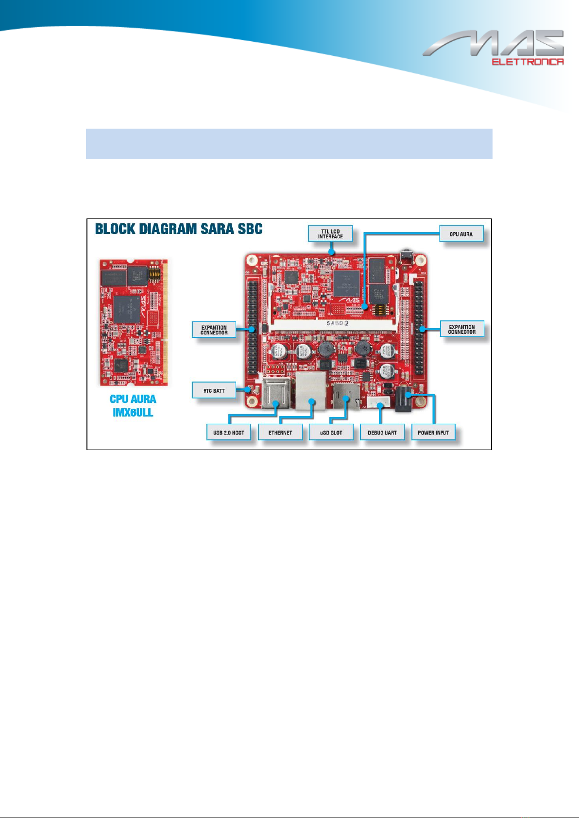
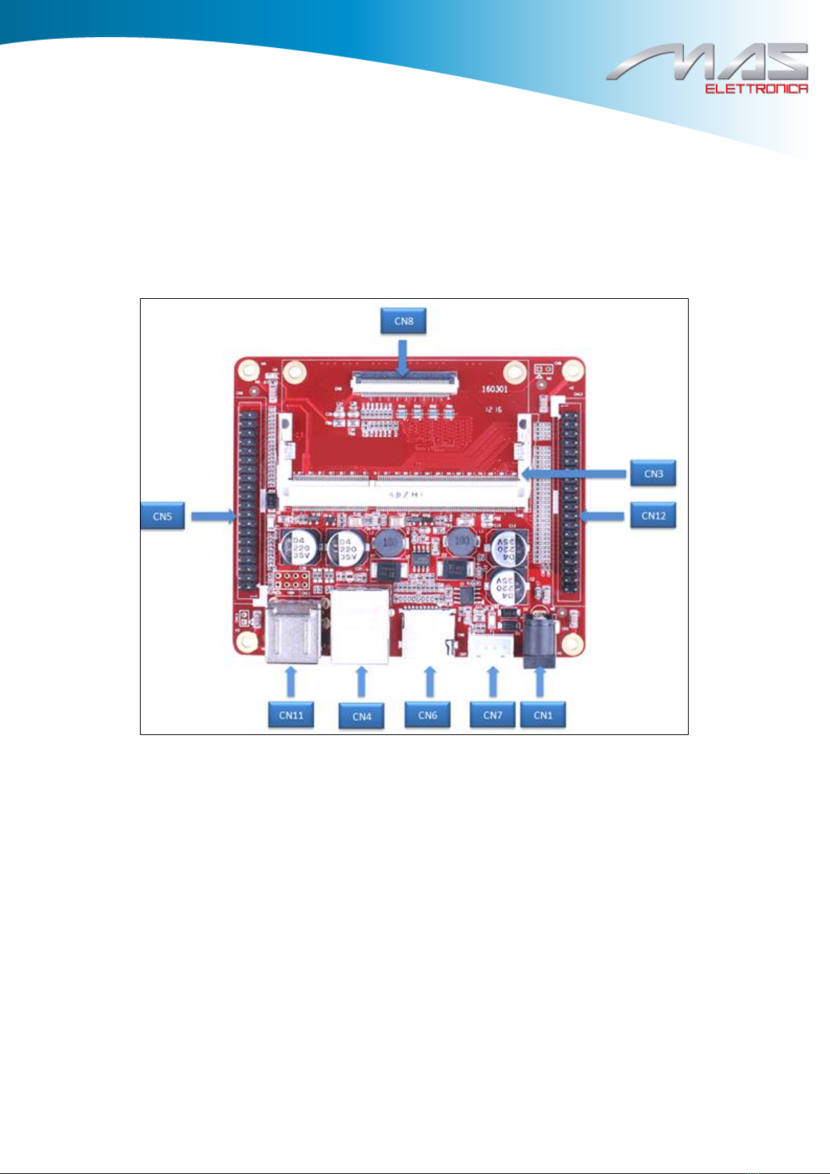
The single board computer SARA which has an expansion board to carry the AURA
i.MX6ULL is one of our design of the base plate . The flexible design allows the fast
and easy way of realizing and upgrading the controller’s capabilities. In additional to
those features offered by AURA i.MX6ULL, the SARA features 6 serial ports (6
TTL), 2 USB Host, 1 Ethernet ports, CAN, PWM, LCD, Touch screen, I2S, I2C, SPI,
GPIOs, RTC and more other peripherals.
The single board targets a wide range of applications, including: HMIs, Digital Signage,
POS, Data Terminal, Medical Devices, Navigation, Industrial Automation,
Entertainment system, Thin Clients, Robotics, Game Console and much more.
1.1.2 Software
The SARA is a ready-to-run platform to support for Linux 4.x, operating systems.
If you care about other Operating System, For more information contact our support.

SARA Hardware User Manual VERSION 1.0
1.2 Product Overview
The following sections list out all the porduct features.
Name
SARA
SARA
SARA
Part Code
SRAS0050
SRAS0060
SRAS0080
CPU Name
IMX6ULL
IMX6ULL
IMX6ULL
CPU Type
ARM Cortex™-A7
ARM Cortex™-A7
ARM Cortex™-A7
CPU Clock
1x
1x
1x
CPU Frequency
800MHz
800MHz
800MHz
RAM DDR3
Micron 512MB@16bit*1
Micron 256MB@16bit*1
Micron 512MB@16bit*1
Flash
GB@8bit*1
eMMC 8GB@8bit*1
eMMC 4GB@8bit*1
PMU
PF3000
PF3000
PF3000
Size
100 x 85 x 19mm
100 x 85 x 19mm
100 x 85 x 19mm
Temperature
0° 70° C
0° 70° C
-0° 70° C
Support OS
Linux 4.X
Linux 4.X
Linux 4.X

Chapter 2 Hardware System
2.1 Block Diagram
Figure 1 SARA Block Diagram
2.2 Main Features
SARA provides the following features and communication interfaces:
■1x RJ45 Ethernet (10/100 Mbit)
■2x USB 2.0 port through on board USB HUB
■1x TF 24-bit
■1x DDR3 STD connector
■1x Digital RGB interface (up to 16 bit colour)
■2x expansion connector with 4x UART (3.3V TTL), 1x I2C, 2x SPI, 4x PWM, 1x
MCASP, 29x GPIOs

SARA Hardware User Manual VERSION 1.0
■1x Debug UART (3.3V TTL)
■1x DC-IN jack with 9.6~14.4V
■LEDs

2.3 Hardware Interfaces
2.3.1 Connector Locations
Figure 3 SARA Interface

SARA Hardware User Manual VERSION 1.0
2.3.2 Core Module Interface (CN3)
Type: DDR3 SO-DIMM
Pin
Signal name
Description
I/O
Power rail
Note
1
VBAT
5V main power supply
P
5V
2
GND
Digital ground
GND
3
VBAT
5V main power supply
P
5V
4
GND
Digital ground
GND
5
VBAT
5V main power supply
P
5V
6
GND
Digital ground
GND
7
VBAT
5V main power supply
P
5V
8
GND
Digital ground
GND
9
NC
Not connected
10
NC
Not connected
11
NC
Not connected
12
NC
Not connected
13
GND
Digital ground
GND
14
VIO_3V3
3.3V main power supply
P
3.3V
15
NC
Not connected
16
VIO_3V3
3.3V main power supply
P
3.3V
17
NC
Not connected
18
NC
Not connected
19
VBATBAKUP
RTC backup power supply
P
3V

Pin
Signal name
Description
I/O
Power rail
Note
20
GND
Digital ground
GND
21
NC
Not connected
22
GND
Digital ground
GND
23
USB1_VBUS
USB1 power supply
P
5V
24
NC
Not connected
25
USB1_ID
Use this pin to detect the ID pin if you use USB
OTG.
I
5V
26
NC
Not connected
27
GPIO_5_4
GPIO
O
3V
28
USB0_ID
Use this pin to detect the ID pin if you use USB
OTG.
I
5V
29
USB1_DM
Negative differential USB signal
I/O
5V
30
GPIO_5_3
GPIO
O
3V
31
USB1_DP
Positive differential USB signal
I/O
5V
32
USB_OTG1_DN
Negative differential USB signal
I/O
5V
33
GND
Digital ground
GND
34
USB_OTG1_DP
Positive differential USB signal
I/O
5V
35
ETH1_TD+
Transmit Data+
I/O
36
GND
Digital ground
GND
37
ETH1_TD-
Transmit Data-
I/O
38
GND
Digital ground
GND
39
NC
Not connected
40
SD_MMC0_DAT0
MMC/SD/SDIO data bus
I/O
3.3V

SARA Hardware User Manual VERSION 1.0
Pin
Signal name
Description
I/O
Power rail
Note
41
NC
Not connected
42
SD_MMC1_DAT1
MMC/SD/SDIO data bus
I/O
3.3V
43
NC
Not connected
44
SD_MMC1_DAT2
MMC/SD/SDIO data bus
I/O
3.3V
45
NC
Not connected
46
SD_MMC1_DAT3
MMC/SD/SDIO data bus
I/O
3.3V
47
NC
Not connected
48
SD_MMC1_CMD
MMC/SD/SDIO command
I/O
3.3V
49
NC
Not connected
50
MMC1_CD
SD card detect
I
3.3V
51
LED_ACT
Link active LED
I
2.5V
52
SD_MMC1_CLK
MMC/SD/SDIO clock
I/O
3.3V
53
LED_LINK
100/1000M linked LED
I
2.5V
54
GND
Digital ground
GND
55
PF3000_SW1AFB_3V3
2.5V power supply
P
2.5V
56
JTAG_nTRST
JTAG TRST
I/O
3.3V
57
NC
Not connected
58
JTAG_TMS
JTAG DATA
I/O
3.3V
59
LCD_DATA2
LCD_DATA2 (gpio)
O
3.3V
60
JTAG_TDI
SPI data
I/O
3.3V
61
LCD_DATA8
LCD_DATA8 (gpio)
O
3.3V
62
JTAG_TCK
JTAG_CLK
I/O
3.3V

Pin
Signal name
Description
I/O
Power rail
Note
63
LCD_DATA9
LCD_DATA9 (gpio)
O
3.3V
64
GND
Digital ground
GND
65
NC
Not connected
66
RESET_OUT
Not connected
67
NC
Not connected
68
PF3000_VLDO4_ADJ
1.8V power supply
P
1.8V
69
NC
Not connected
70
JTAG_SYS_RST#
71
GND
Digital ground
GND
72
PF3000_SW1AFB_3V3
MMC/SD/SDIO power supply
P
3.3V
73
GND
Digital ground
GND
74
BUTT_RESET
Reset input
I/O
3.3V
75
UART6_TX
UART transmit data
O
3.3V
76
NC
Not connected
77
UART6_RX
UART receive data
I
3.3V
78
EXT_QSPIA_SCLK
Not connected
79
GND
Digital ground
GND
80
EXT_QSPIA_DATA0
Not connected
81
NC
Not connected
82
EXT_QSPIA_DATA1
Not connected
83
GND
Digital ground
GND
84
EXT_QSPIA_DATA2
Not connected

SARA Hardware User Manual VERSION 1.0
Pin
Signal name
Description
I/O
Power rail
Note
85
I2C1_SDA
I2C1 DATA
O
3.3V
86
EXT_QSPIA_DATA3
Not connected
87
I2C1_SCL
I2C1 CLOCK
I
3.3V
88
EXT_QSPIA_nSS
Not connected
89
GND
Digital ground
GND
90
NC
Not connected
91
NC
Not connected
92
GND
Digital ground
GND
93
GND
Digital ground
GND
94
UART1_TX
UART transmit data
O
3.3V
95
UART3_TX
UART transmit data
O
3.3V
96
UART1_RX
UART receive data
I
3.3V
97
UART3_RX
UART receive data
I
3.3V
98
GND
Digital ground
GND
99
UART2_RX
UART receive data
I
3.3V
100
NC
Not connected
101
UART2_TX
UART transmit data
O
3.3V
102
NC
Not connected
103
GND
Digital ground
GND
104
JTAG_TDO
NC
O
3.3V
105
NC
Not connected
106
ENET2_TX_CLK
ENET2_TX_CLK
O
3.3V

Pin
Signal name
Description
I/O
Power rail
Note
107
GND
Digital ground
GND
108
ENET2_TX_TXEN
ENET2_TX_TXEN/
O
3.3V
109
ENET2_RXD0
ENET2_RXD0/
O
3.3V
110
ENET2_TXD1
ENET2_TXD1/
O
3.3V
111
ENET2_TX_CLK
ENET2_TX_CLK/
O
3.3V
112
NC
Not connected
113
GND
Digital ground
GND
114
LCD_DATA0
LCD data bus
115
NC
Not Connected
116
LCD_DATA1
LCD data bus
117
GND
Digital ground
GND
118
NC
Not connected
119
I2C2_SCL
I2C clock
I/O
3.3V
120
NC
Not connected
121
I2C2_SDA
I2C data
I/O
3.3V
122
LCD_DATA18
LCD data bus
123
GND
Digital ground
GND
124
NC
Not connected
125
NC
Not connected
126
NC
Not connected
127
GND
Digital ground
GND
128
GND
Digital ground
GND

SARA Hardware User Manual VERSION 1.0
Pin
Signal name
Description
I/O
Power rail
Note
129
NC
Not connected
130
GND
Digital ground
GND
131
NC
Not connected
132
NC
Not connected
133
NC
Not connected
134
GND
Digital ground
GND
135
NC
Not connected
136
SAI1_MCLK
AUDIO master clock
I/O
3.3V
137
NC
Not connected
138
SAI1_TX_BCLK
McASP0 transmit bit clock
I/O
3.3V
139
GND
Digital ground
GND
140
SAI1_TX_SYNC
McASP0 transmit frame sync
I/O
3.3V
141
ADC4
Analog input/output
I/O
3.3V
142
SAI1_RX_DATA
McASP0 serial data (in/out)
I/O
3.3V
143
ADC3
Analog input/output
I/O
3.3V
144
SAI1_TX_DATA
McASP0 serial data (in/out)
I/O
3.3V
145
ADC2
Analog input/output
I/O
3.3V
146
GND
Digital ground
GND
147
ADC1
Analog input/output
I/O
3.3V
148
ENET2_TXD0
I
3.3V
149
GND
Digital ground
GND
150
ENET2_CRS_DV 10
I
3.3V

Pin
Signal name
Description
I/O
Power rail
Note
151
NC
Not connected
152
NC
Not connected
153
NC
Not connected
154
GND
Digital ground
GND
155
GND
Digital ground
GND
156
ENET2_RXER
GPIO
I/O
3.3V
157
LCD_DATA3
LCD data bus
I/O
3.3V
158
SAI1_RX_SYNC
GPIO
I/O
3.3V
159
LCD_DATA4
LCD data bus
I/O
3.3V
160
GND
Digital ground
GND
161
LCD_DATA5
LCD data bus
I/O
3.3V
162
SAI1_RX_BCLK
GPIO
I/O
3.3V
163
LCD_DATA6
LCD data bus
I/O
3.3V
164
NC
Not connected
165
LCD_DATA7
LCD data bus
I/O
3.3V
166
GND
Digital ground
GND
167
LCD_DATA10
LCD data bus
I/O
3.3V
168
UART3_RTS
GPIO
I/O
3.3V
169
LCD_DATA11
LCD data bus
I/O
3.3V
170
UART3_CTS
GPIO
I/O
3.3V
171
LCD_DATA12
LCD data bus
I/O
3.3V
172
GND
Digital ground
GND

SARA Hardware User Manual VERSION 1.0
Pin
Signal name
Description
I/O
Power rail
Note
173
LCD_DATA13
LCD data bus
I/O
3.3V
174
UART2_RTS
GPIO
I/O
3.3V
175
LCD_DATA14
LCD data bus
I/O
3.3V
176
UART2_CTS
GPIO
I/O
3.3V
177
LCD_DATA15
LCD data bus
I/O
3.3V
178
GND
Digital ground
GND
179
LCD_DATA19
LCD data bus
I/O
3.3V
180
GPIO5_0
GPIO
I/O
3.3V
181
LCD_DATA20
LCD data bus
I/O
3.3V
182
GPIO5_8
GPIO
I/O
3.3V
183
LCD_DATA21
LCD Data Bus
I/O
3.3V
184
GPIO5_1
GPIO
I/O
3.3V
185
LCD_DATA22
LCD data bus
I/O
3.3V
186
GPIO5_5
GPIO
I/O
3.3V
187
LCD_DATA23
LCD data bus
I/O
3.3V
188
GPIO5_6
GPIO
I/O
3.3V
189
GND
Digital ground
GND
190
GPIO5_7
GPIO
I/O
3.3V
191
LCD_PCLK
LCD pixel clock
O
3.3V
192
CSI_VSYNC
GPIO
I/O
3.3V
193
LCD_VSYNC
LCD vertical sync
O
3.3V

Pin
Signal name
Description
I/O
Power rail
Note
194
CSI_HSYNC
GPIO
I/O
3.3V
195
LCD_HSYNC
LCD horizontal sync
O
3.3V
196
CSI_DATA0
GPIO
I/O
3.3V
197
LCD_EN
LCD enable
O
3.3V
198
LCD_DATA17
GPIO
I/O
3.3V
199
GND
Digital ground
GND
200
LCD_DATA16
GPIO
I/O
3.3V
201
LED_PWM
LCD PWM Control
O
3.3V
202
GPIO5_9
GPIO
I/O
3.3V
203
GND
Digital ground
GND
204
GND
Digital ground
GND
2.3.3 Ethernet Interface (CN4)
Type: RJ45
Pin
Signal name
Description
I/O
Power rail
Note
1
TD1+
Transmit Data1+
I/O
2
TD1-
Transmit Data1-
I/O
3
TD2+
Transmit Data2+
I/O
4
TXD2-
Transmit Data2-
I/O
5
TCT
Transmit common terminal
6
RCT
Receive common terminal
7
RD1+
Receive Data1+
I/O

SARA Hardware User Manual VERSION 1.0
Pin
Signal name
Description
I/O
Power rail
Note
8
RD1-
Receive Data1-
I/O
9
RD2+
Receive Data2+
I/O
10
RD2-
Receive Data2-
I/O
11
GRLA
3.3V Power Supply
P
3.3V
12
GRLC
Link active LED
13
YELC
100M linked LED
14
YELA
3.3V Power Supply
P
3.3V
15
GND
Digital ground
GND
16
GND
Digital ground
GND
2.3.4 Expansion Interface (CN5)
Type: Pin Header 2x20 2.54mm pitch
Pin
Signal name
Description
I/O
Power rail
Note
1
VIO_3V3
3.3V main power supply
P
3.3V
2
VCC5V
5V power supply
P
5V
3
I2C1_SDA
I2c1 data
O
3.3V
4
VCC5V
5V power supply
P
5V
5
I2C1_SCL
I2c1 clock
I
3.3V
6
GND
Digital ground
GND
7
ENET2_RXER
GPIO
I/O
3.3V
8
UART6_TX
UART transmit data
O
3.3V
9
GND
Digital ground
GND
10
UART6_RX
UART receive data
I
3.3V

Pin
Signal name
Description
I/O
Power rail
Note
11
NC
Address latch enable
O
3.3V
12
LCD_DATA2
Read enable
O
3.3V
13
NC
Write enable
O
3.3V
14
GND
Digital ground
GND
15
LCD_DATA9
Command latch enable
O
3.3V
16
ENET1_RXD0
Ready/busy
I
3.3V
17
VIO_3V3
3.3V main power supply
P
3.3V
18
NC
Write project
O
3.3V
19
JTAG_TMS
JTAG
I/O
3.3V
20
GND
Digital ground
GND
21
JTAG_TDI
JTAG
I/O
3.3V
22
LCD_DATA8
GPIO
O
3.3V
23
JTAG_TRST
JTAG
I/O
3.3V
24
JTAG_TCK
JTAG
I/O
3.3V
25
GND
Digital ground
GND
26
UART3_RX
UART receive data
I
3.3V
27
LCD_DATA17
GPIO
I/O
3.3V
28
LCD_DATA16
LCD DATA16
I/O
3.3V
29
SAI1_MCLK
McASP0 transmit master clock
I/O
3.3V
30
GND
Digital ground
GND
31
SAI1_TX_BCLK
McASP0 transmit bit clock
I/O
3.3V
32
GPIO5_9
GPIO
I/O
3.3V
Table of contents
Popular Desktop manuals by other brands

Panasonic
Panasonic CF-T1 Series Reference manual

Lenovo
Lenovo ThinkCentre Edge 71 Benutzerhandbuch

Amiga
Amiga A4000 user guide

J.Burrows
J.Burrows STILFORD JBSTIHA14 Assembly instructions

Sony
Sony VPCF23B9E user guide

Lenovo
Lenovo 6072CC3 - Thinkcentre M57 2.33G2gb 80Gb Dvdrom... Hardware installation and replacement guide