Micrel RadioWire MICRF507 User manual

MICRF507
470MHz to 510MHz Low-Power FSK
Transceiver with +10dBm Power Amplifier
RadioWire is a registered trademark of Micrel, Inc.
Micrel Inc. • 2180 Fortune Drive • San Jose, CA 95131 • USA • tel +1 (408) 944-0800 • fax + 1 (408) 474-1000 • http://www.micrel.com
October 2, 2013
Revision 2.2
General Description
The MICRF507 is a fully-integrated FSK transceiver with
+10dBm power amplifier and transmit/receive switch. The
device is targeted at automated meter reading (AMR)
applications in the China Short Range Device (SRD)
frequency band of 470MHz to 510MHz. The device
supports data rates up to 20kbps with PLL divider
modulation and up to 200kbps with VCO modulation. The
receiver achieves a sensitivity of -113dBm at a data rate of
2.4kbps while only consuming 12mA of supply current.
The integrated power amplifier (PA) delivers +10dBm of
output power while only consuming 21.5mA of supply
current. Power down supply current is a low 0.2µA while
retaining register information and a low 280µA in standby
mode where only the crystal oscillator is enabled.
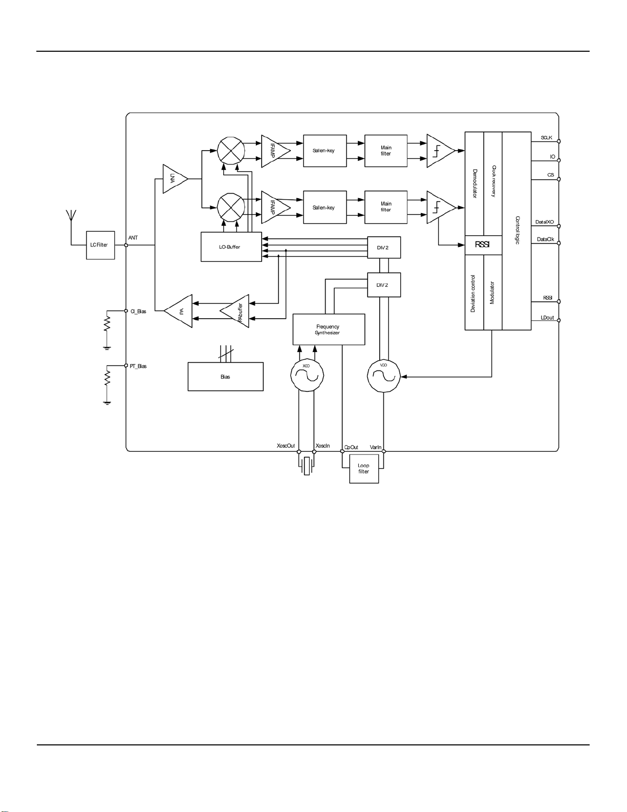
The receiver of the MICRF507 utilizes a Zero IF (ZIF) I/Q
architecture, integrating a low-noise amplifier (LNA) with
bypass mode, I/Q quadrature mixers, three-pole Sallen-
Key IF channel pre-filters, and six-pole elliptic switched
capacitor IF filters, providing excellent selectivity, adjacent
channel rejection and blocking performance. FSK
demodulation is implemented digitally and a synchronizer,
when enabled, recovers the received bit clock. A receive
signal strength indicator (RSSI) circuit indicates the
received signal level over a 50dB range. An integrated
Frequency Error Estimator (FEE) and crystal tuning
capability allow fine tuning of the RF frequency.
The transmitter of the MICRF507 consists of an FSK
modulator and power amplifier with output power
adjustable from +10dBm to -3.5dBm in seven steps.
Modulation can be achieved by applying two sets of PLL
divider ratios or through direct VCO modulation by varying
VCO tank capacitance.
The MICRF507 requires a 2.0V to 2.5V supply voltage,
operates over the -40˚C to +85˚C temperature range, and
is available in a 32-pin QFN package.
RadioWire®
Features
•-113dBm sensitivity at 2.4kbps encoded bit rate
•+10dBm power amplifier with seven gain steps
•12mA receive supply current
•21.5mA transmit supply current at +10dBm
•0.2μA power down current (registers retain settings)
•280µA standby current (crystal oscillator enabled)
•Data rates up to 20kbps with PLL divider modulation
•Data rates up to 200kbps with VCO modulation
•Integrated transmit and receive (T/R) switch
•LNA with bypass mode
•Zero IF I/Q receiver architecture
•IF pre-amplifiers with DC-offset removal
•Three-pole Sallen-Key IF channel low-pass pre-filter
•Six-pole elliptic switched capacitor IF low-pass filter
•50kHz to 350kHz programmable baseband bandwidth
•59dB blocking at ±1MHz offset
•53dB adjacent channel rejection at ±500kHz offset
•FSK digital demodulator with clock recovery
•50dB Received Signal Strength Indicator (RSSI)
•Frequency Error Estimator (FEE)
•Reference crystal tuning capability
•2.0 to 2.5V supply voltage range
•-40˚C to +85˚C operating temperature range
•Available in 32-pin QFN package
(5.0mm × 5.0mm × 0.85mm)
Applications
•China Short Range Device (SRD) Communications
•Automated Meter Reading (AMR)
•Advanced Metering Infrastructure (AMI)
•Wireless Remote Meter Reading

Micrel, Inc.
MICRF507
October 2, 2013
2
Revision 2.2
RadioWire®FSK Transceiver Selection Guide................................................................................................................4
Ordering Information .........................................................................................................................................................4
Pin Configuration...............................................................................................................................................................4
Pin Description...................................................................................................................................................................4
Block Diagram....................................................................................................................................................................6
Absolute Maximum Ratings..............................................................................................................................................7
Operating Ratings..............................................................................................................................................................7
Electrical Characteristics ..................................................................................................................................................7
Functional Description ....................................................................................................................................................10
Control (3-wire) Interface ......................................................................................................................................10
Reading.................................................................................................................................................................13
Control Interface Timing........................................................................................................................................14
Power-on Reset ....................................................................................................................................................14
Clock Generation .............................................................................................................................................................15
Crystal Oscillator (XCO) ..................................................................................................................................................16
BITSYNC_CLK (Receiver Bit Synchronization Clock)..........................................................................................17
BITRATE_CLK (Transmitter Bit Rate Clock) ........................................................................................................17
MODULATOR_CLK (VCO Modulator Clock)........................................................................................................17
Data Interface and Bit Synchronization.........................................................................................................................17
Sync_en = 0 ..........................................................................................................................................................19
Sync_en = 1 ..........................................................................................................................................................19
Additional Considerations in the Use of Synchronizer (Sync_en = 1)..................................................................19
Frequency Synthesizer....................................................................................................................................................20
VCO.......................................................................................................................................................................22
Charge Pump........................................................................................................................................................22
PLL Filter...............................................................................................................................................................22
Lock Detect ...........................................................................................................................................................23
Receiver ............................................................................................................................................................................24
Front End...............................................................................................................................................................24
Sallen-Key Filters..................................................................................................................................................25
Switched Capacitor Filter......................................................................................................................................25
RSSI......................................................................................................................................................................25
FEE .......................................................................................................................................................................26
XCOtune Procedure Example.........................................................................................................................................27
Transmitter........................................................................................................................................................................28
Power Amplifier.....................................................................................................................................................28
Frequency Modulation...........................................................................................................................................29
Divider Modulation ................................................................................................................................................30
VCO Modulation and the Modulator......................................................................................................................30
Modulator Filter .....................................................................................................................................................32
System Modes and Initialization.....................................................................................................................................33
Start-up and Initialization.......................................................................................................................................33
Modes of Operation...............................................................................................................................................33
Mode Transitions...................................................................................................................................................33
Message Coding and Formatting ...................................................................................................................................34
DC Balanced Line Coding.....................................................................................................................................34
Message Formatting: Preamble............................................................................................................................34
Typical Application ..........................................................................................................................................................35

Micrel, Inc.
MICRF507
October 2, 2013
3
Revision 2.2
Bill of Materials.................................................................................................................................................................36
Layout Considerations ....................................................................................................................................................37
Layer Definition .....................................................................................................................................................37
Grounding..............................................................................................................................................................37
RF Traces..............................................................................................................................................................37
Supply Routing......................................................................................................................................................37
PLL Loop Filter......................................................................................................................................................37
Overview of Programming Bits.......................................................................................................................................38
Detailed Description of Programming Bits....................................................................................................................39
Package Information and Recommended Landing Pattern.........................................................................................46

Micrel, Inc.
MICRF507
October 2, 2013
4
Revision 2.2
RadioWire®FSK Transceiver Selection Guide
Part Number Frequency Range Maximum Data
Rate Receive
Current Supply Voltage Transmit Current Package
MICRF505 850MHz to 950MHz 200kbps 13.5mA 2.0 to 2.5V 28mA QFN-32
MICRF505L 850MHz to 950MHz 200kbps 13.5mA 2.25 to 5.5V 28mA QFN-32
MICRF506 410MHz to 450MHz 200kbps 12mA 2.0 to 2.5V 21.5mA QFN-32
MICRF507 470MHz to 510MHz 200kbps 12mA 2.0 to 2.5V 21.5mA QFN-32
Ordering Information
Part Number Junction Temperature Range Package
MICRF507YML TR -40° to +85°C Pb-Free 32-Pin QFN
Pin Configuration
32-Pin QFN
Pin Description
Pin Number
Pin Name
Type
Pin Function
1 RFGND LNA and PA ground.
2 PTATBIAS O Connection for bias resistor.
3 RFVDD LNA and PA power supply.
4 RFGND LNA and PA ground.
5 ANT I/O Antenna Input/Output.
6 RFGND LNA and PA ground.
7 RFGND LNA and PA ground.

Micrel, Inc.
MICRF507
October 2, 2013
5
Revision 2.2
Pin Description (Continued)
Pin Number
Pin Name
Type
Pin Function
8, 16, 17, 32 NC No connect. Leave these pins floating.
9 CIBIAS O Connection for bias resistor.
10 IFVDD IF/mixer power supply.
11 IFGND IF/mixer ground.
12 ICHOUT O Test pin.
13 QCHOUT O Test pin.
14 RSSI O Received signal strength indicator.
15 LD O PLL lock indicator.
18 DATACLK O RX/TX data clock output.
19 DATAIXO I/O RX/TX data input/output.
20 IO I/O 3-wire interface data in/output
21 SCLK I 3-wire interface serial clock.
22 CS I 3-wire interface chip select.
23 XTALIN I Crystal oscillator input.
24 XTALOUT I/O Crystal oscillator output or external reference input.
25 DIGVDD Digital power supply.
26 DIGGND Digital ground.
27 CPOUT O PLL charge pump output.
28 GND Substrate ground.
29 VARIN I VCO varactor tune voltage input.
30 VCOGND VCO ground.
31 VCOVDD VCO power supply.
Exposed Paddle Ground.
Micrel, Inc.
MICRF507
October 2, 2013
6
Revision 2.2
Block Diagram
Micrel, Inc.
MICRF507
October 2, 2013
7
Revision 2.2
Absolute Maximum Ratings(1)
Supply Voltage (VDD)...................................................+2.7V
Voltage on any pin (GND = 0V)..............-0.3V to +2.7V
Lead Temperature (soldering, 4sec.).........................300°C
Storage Temperature (Ts)..........................-55°C to +150°C
ESD Rating(3)..................................................................2kV
Operating Ratings(2)
Supply Voltage (VIN)..................................+2.0V to +2.5V
RF Frequencies ................................470MHz to 510MHz
Encoded Bit Rate.................................................200kbps
Ambient Temperature (TA).......................–40°C to +85°C
Package Thermal Resistance
32-Pin QFN (θJA) .........................................41.7°C/W
Electrical Characteristics(4)
fRF = 490MHz, fXTAL = 16MHz, MICRF507 Development Board, Modulation type = closed-loop VCO modulation, Sync_en bit = 1,
VDD = 2.5V; TA= 25°C, the term “bit rate” refers to encoded bit rate throughout the EC table (see Figure 24), bold values indicate
–40°C< TA< +85°C, unless noted.
Symbol Parameter Condition Min Typ Max Units
fRF RF Frequency Operating Range 470 510 MHz
VDD Power Supply 2.5 V
Power Down Current 0.2
3
µA
Standby Current 280 µA
VCO and PLL Section
Reference Frequency
4
40
MHz
PLL Lock Time, 3kHz Bandwidth 490MHz to 490.5MHz 0.7 ms
485MHz to 495MHz 1.3 ms
PLL Lock Time, 20kHz Bandwidth 490MHz to 490.5MHz 0.3 ms
Switch Time, 3kHz Loop Bandwidth
Rx – Tx 1.0
ms
Tx – Rx 1.0
Standby to Rx 1.0
Standby to Tx 1.0
Crystal Oscillator Start-Up Time With MICRF507 development
board BOM 1.0 ms
Charge Pump Current VCPOUT = 1.1V, CP_HI = 0
100
125
170
µA
VCPOUT = 1.1V, CP_HI = 1 420 500 680 µA
Transmit Section
POUT Output Power RLOAD = 50Ω, PA[2:0] = 111 10 dBm
RLOAD = 50Ω, PA[2:0] = 001 -3.5 dBm
Output Power Variation Relative to
VDD = 2.5V, TA= 25°C Over temperature range ±1 dB
VDD = 2.0V -2 dB
Transmit Mode Current
Consumption
RLOAD = 50Ω, PA[2:0] = 111 21.5 mA
RLOAD = 50Ω, PA[2:0] = 001 10.5 mA
RLOAD = 50Ω, PA[2:0] = 000 8.0 mA
Notes:
1. Exceeding the absolute maximum rating may damage the device.
2. The device is not guaranteed to function outside its operating rating.
3. Devices are ESD sensitive. Handling precautions recommended. Human body model; 1.5k in series with 100pF.
4. Specification for packaged product only.
Micrel, Inc.
MICRF507
October 2, 2013
8
Revision 2.2
Electrical Characteristics(4)(Continued)
fRF = 490MHz, fXTAL = 16MHz, MICRF507 Development Board, Modulation type = closed-loop VCO modulation, Sync_en bit = 1,
VDD = 2.5V; TA= 25°C, the term “bit rate” refers to encoded bit rate throughout the EC table (see Figure 24), bold values indicate
–40°C< TA< +85°C, unless noted.
Symbol Parameter Condition Min Typ Max Units
Single-Sided Frequency
Deviation(5)10 250 kHz
Maximum Bit Rate VCO modulation 200 kbps
Divider modulation 20 kbps
Occupied Bandwidth(5)38.4kbps, β= 2, 20dBc 140 kHz
125kbps, β= 2, 20dBc 550 kHz
200kbps, β= 2, 20dBc 800 kHz
2
nd
Harmonic
(5)
-43 -36 dBm
3
rd
Harmonic
(5)
-59 -36 dBm
Spurious Emission in Restricted
Bands < 1GHz(5)-54 dBm
Spurious Emission < 1GHz
(5)
-36 dBm
Spurious Emission > 1GHz
(5)
-30 dBm
Receive Section
Rx Current Consumption
All Functions on 12
mA
LNA bypassed 10.3
Switch cap filter bypassed, LNA on 9.8
Both switch cap filter and LNA
bypassed 8
Rx Current Consumption Variation Over temperature 2 mA
Receiver Sensitivity (BER 10-3)
2.4kbps, β= 16 -113
dBm
4.8kbps, β= 16 -111
19.2kbps, β= 4 -107
38.4kbps, β= 4 -104
76.8kbps, β= 2 -101
125kbps, β= 2 -100
200kbps, β= 2 -97
Receiver Maximum Input Power
125kbps, 125kHz deviation, LNA on +7
dBm
125kbps, 125kHz deviation, LNA
bypassed +12
20kbps, 40kHz deviation +2
Receiver Sensitivity Tolerance Over temperature 2 dB
Over power supply range 1 dB
Receiver Baseband Bandwidth 50 350 kHz
Co-Channel Rejection, BER = 10-3 19.2kbps, β= 6, PF_FC[1:0] = 01,
fCUT = 133kHz -8 dB
Note:
5. Guaranteed by design.

Micrel, Inc.
MICRF507
October 2, 2013
9
Revision 2.2
Electrical Characteristics(4)(Continued)
fRF = 490MHz, fXTAL = 16MHz, MICRF507 Development Board, Modulation type = closed-loop VCO modulation, Sync_en bit = 1,
VDD = 2.5V; TA= 25°C, the term “bit rate” refers to encoded bit rate throughout the EC table (see Figure 24), bold values indicate
–40°C< TA< +85°C, unless noted.
Symbol Parameter Condition Min. Typ. Max. Units
Adjacent Channel Rejection, both
interferer and desired signal are
modulated at 19.2 kbps encoded
bit rate, β= 6, PF_FC[1:0] = 01,
fCUT = 133kHz, BER = 10-3
±500kHz spacing 53 dB
±1MHz spacing 58 dB
CW Blocking above desired
signal, desired signal is modulated
at 19.2kbps, β= 6, 3dB above
sensitivity, PF_FC[1:0] = 01,
fCUT = 133kHz, BER = 10-3
±1MHz 59 dB
±2MHz 60 dB
±5MHz 47 dB
±10MHz 60 dB
P1dB 1dB Compression -34 dBm
Input IP3 2 tones with 1MHz separation -25 dBm
LO Leakage -90 dBm
Spurious Emission(5)<1GHz -57 dBm
>1GHz -47 dBm
Input Impedance with no matching
components 33+7j Ω
RSSI Dynamic Range 50 dB
RSSI Output Range PIN = -110dBm 0.9 V
PIN = -60dBm 2 V
Digital Inputs/Outputs
VIH Logic Input High 0.7*VDD VDD V
VIL Logic Input Low
0
0.3*V
DD
V
Clock/Data Frequency
(5)
10 MHz
Clock/Data Duty Cycle
(5)
45 55 %

Micrel, Inc.
MICRF507
October 2, 2013
10
Revision 2.2
Functional Description
Control (3-wire) Interface
General
The MICRF507 operation is controlled through a set of 8-
bit registers. The chip has a total of 23 readable registers
(addresses 0-22) of which 22 (addresses 0-21) are
writeable. Through this register set, the user can set the
MICRF507 in transmit or receive mode, program the
carrier frequency, and select a bit rate, among other
options.
Table 1 identifies all register bits. Table 26 gives more
detail and Table 27 shows the register fields grouped by
category, with don’t-care and mandatory bits omitted.
Some bits shown as ‘0’ or ‘1’ are mandatory bits and must
always be written with the values given. Other bits marked
as “-“ are “don’t care” bits.
Registers are accessed serially through the control
interface consisting of the CS, IO, and SCLK pins.
Positive-going pulses at SCLK serve to clock bits in and
out of IO at a rate determined by the user. When IO is an
input, falling edges of SCLK strobe each bit in; when IO is
an output, each bit appears at IO after the rising edge of
SCLK.
The IO is an input for entry of starting addresses, the R/W
bit, and bytes being written to registers, and an output for
bytes read from registers.
CS enables transactions at the control interface, active
high. Transitions at the other two pins are ignored when
CS is low. This allows the MICRF507 to share SCLK and
IO with other devices as long as they have separate CS
lines.
To start a transaction (with SCLK and CS initially low),
bring CS high. To end a transaction (with SCLK low), bring
CS low.
To write a bit into IO (when IO is an input); first bring SCLK
high and drive IO with the bit level to be input (in either
order, or simultaneously). Then bring SCLK low.
To read a bit out of IO (when IO is an output); first bring
SCLK high and read the level on IO. Then bring SCLK low
(in either order, or simultaneously).
The first byte to be clocked in during a transaction is made
of seven bits (MSB first) of register address followed by
the R/W bit, 0 for write, 1 for read. Then, one or more
bytes to be written to or read from registers are clocked in
or out respectively, always MSB first.

Micrel, Inc.
MICRF507
October 2, 2013
11
Revision 2.2
Adr Data Field
A6…A0 D7 D6 D5 D4 D3 D2 D1 D0
0000000 LNA_by PA2 PA1 PA0 Sync_en Mode1 Mode0 ’1’
0000001 Modulation1 Modulation0 ‘0’ ‘0’ RSSI_en LD_en PF_FC1 PF_FC0
0000010 CP_HI SC_by ‘0’ PA_By OUTS3 OUTS2 OUTS1 OUTS0
0000011 ‘1’ ‘1’ ‘0’ VCO_IB2 VCO_IB1 VCO_IB0 VCO_freq1 VCO_freq0
0000100 Mod_F2 Mod_F1 Mod_F0 Mod_I4 Mod_I3 Mod_I2 Mod_I1 Mod_I0
0000101 - - ‘0’ ‘1’ Mod_A3 Mod_A2 Mod_A1 Mod_A0
0000110 - Mod_clkS2 Mod_clkS1 Mod_clkS0 BitSync_clkS2 BitSync_clkS1 BitSync_clkS0 BitRate_clkS2
0000111 BitRate_clkS1 BitRate_clkS0 RefClk_K5 RefClk_K4 RefClk_K3 RefClk_K2 RefClk_K1 RefClk_K0
0001000 ‘1’ ‘1’ ‘0’ ScClk4 ScClk3 ScClk2 ScClk1 ScClk0
0001001 ‘0’ ‘0’ ‘1’ XCOtune4 XCOtune3 XCOtune2 XCOtune1 XCOtune0
0001010 - - A0_5 A0_4 A0_3 A0_2 A0_1 A0_0
0001011 - - - - N0_11 N0_10 N0_9 N0_8
0001100 N0_7 N0_6 N0_5 N0_4 N0_3 N0_2 N0_1 N0_0
0001101 - - - - M0_11 M0_10 M0_9 M0_8
0001110 M0_7 M0_6 M0_5 M0_4 M0_3 M0_2 M0_1 M0_0
0001111 - - A1_5 A1_4 A1_3 A1_2 A1_1 A1_0
0010000 - - - - N1_11 N1_10 N1_9 N1_8
0010001 N1_7 N1_6 N1_5 N1_4 N1_3 N1_2 N1_1 N1_0
0010010 - - - - M1_11 M1_10 M1_9 M1_8
0010011 M1_7 M1_6 M1_5 M1_4 M1_3 M1_2 M1_1 M1_0
0010100 ‘1’ ‘0’ ‘1’ ‘0’ ‘0’ ‘0’ ‘1’ ‘1’
0010101 - - - - FEEC_3 FEEC_2 FEEC_1 FEEC_0
0010110 FEE_7 FEE_6 FEE_5 FEE_4 FEE_3 FEE_2 FEE_1 FEE_0
Names of programming bits. Unused bits (“-“) and mandatory bits (“1” or “0”) are shown. Changes to mandatory bits may cause
malfunction.
Table 1. Control Registers
Micrel, Inc.
MICRF507
October 2, 2013
12
Revision 2.2
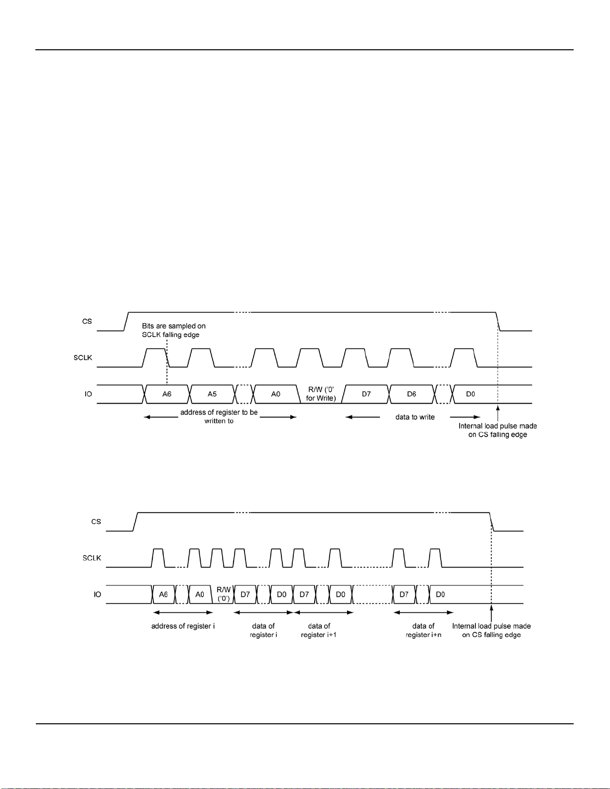
Writing
This method is used to write either to one register (see
Figure 1), or any number of registers with consecutive
addresses up to all 22 writeable registers (see Figure 2) in
a single transaction.
Procedure:
•Bring CS active (high). IO is initially an input (and
remains so for the duration of the transaction).
•Clock in a byte consisting of the address bits and
the R/W bit. The first seven bits are the address
(starting with MSB) of the register, or the first
register if more than one, to be written. The eighth
bit is the R/W bit, which is 0 as this is a write
operation.
•Clock in one or more bytes, MSB of each byte
first.
•Bring CS low to end the transaction.
Bits passing through IO are clocked serially into pre-
buffers, then transferred in parallel to the actual registers
upon de-assertion of CS.
Figure 1. Writing a Byte into a Register
Figure 2. Writing Bytes into n+1 Registers at Consecutive Addresses Starting with Address i

Micrel, Inc.
MICRF507
October 2, 2013
13
Revision 2.2
Reading
Any number of registers with consecutive addresses, from
one up to all 23, can be read.
Procedure:
•Bring CS active (high). IO is initially an input.
•Clock in a byte consisting of the address bits and
the R/W bit. The first seven bits are the address
(starting with MSB) of the register, or the first
register if more than one, to be read. The eighth
bit is the R/W bit, which is 1 as this is a read
operation. After the R/W bit is clocked in (falling
edge of SCLK), the next rising edge on SCLK will
enable IO as an output for the duration of the
transaction.
•Clock out 8 bits per register (one or more) to be
read through IO, MSB first. Rising edges of SCLK
bring each bit to IO. The user can then
conveniently sample the bit at the next falling edge
of SCLK.
•Bring CS low to end the transaction. IO reverts to
being an input.
Figure 3 shows how to read one register. To read more
registers at consecutive addresses, continue pulsing SCLK
eight times for each register to be read before de-asserting
CS.
Figure 3. Reading a Byte from a Register
Figure 4. Definitions of Control Interface Timing Parameters
Micrel, Inc.
MICRF507
October 2, 2013
14
Revision 2.2
Control Interface Timing
Figure 4 and Table 2 give the timing specifications for the
control interface.
When in Receive or Transmit mode (but not Power-down
or Standby mode), an additional timing constraint applies:
elapsed time between falling edges of CS must be a
minimum of 2/fc, where fcis the synthesizer’s comparison
frequency (also called phase detector frequency). fc=
fXCO/M,
XCO
XCO
c
f2M
time
min
M
f
f
=
=
where M = M0 when receiving or transmitting with VCO
modulation, and M = max{M0, M1} when transmitting with
divider modulation.
Symbol
Parameter
Values
Units
Min. Typ. Max.
Thigh Min. high time of
SCLK 20 ns
Tlow Min. low time of
SCLK 20 ns
tfall Fall time of SCLK 1 µs
trise Rise time of SCLK 1 µs
Tcsr
Time from rising
edge of CS to
falling edge of
SCLK
50 ns
Tcsf
Min. delay from
rising edge of CS
to rising edge of
SCLK
25 ns
Twrite
Min. delay from
valid IO to falling
edge of SCLK
during a write
operation
20 ns
Tread
Min. delay from
rising edge of
SCLK to valid IO
during a read
operation
(assuming load
capacitance of IO
is 25pF)
75 ns
tPOR Power on Reset
time 4.6 9
ms
Table 1. Control Interface Timing
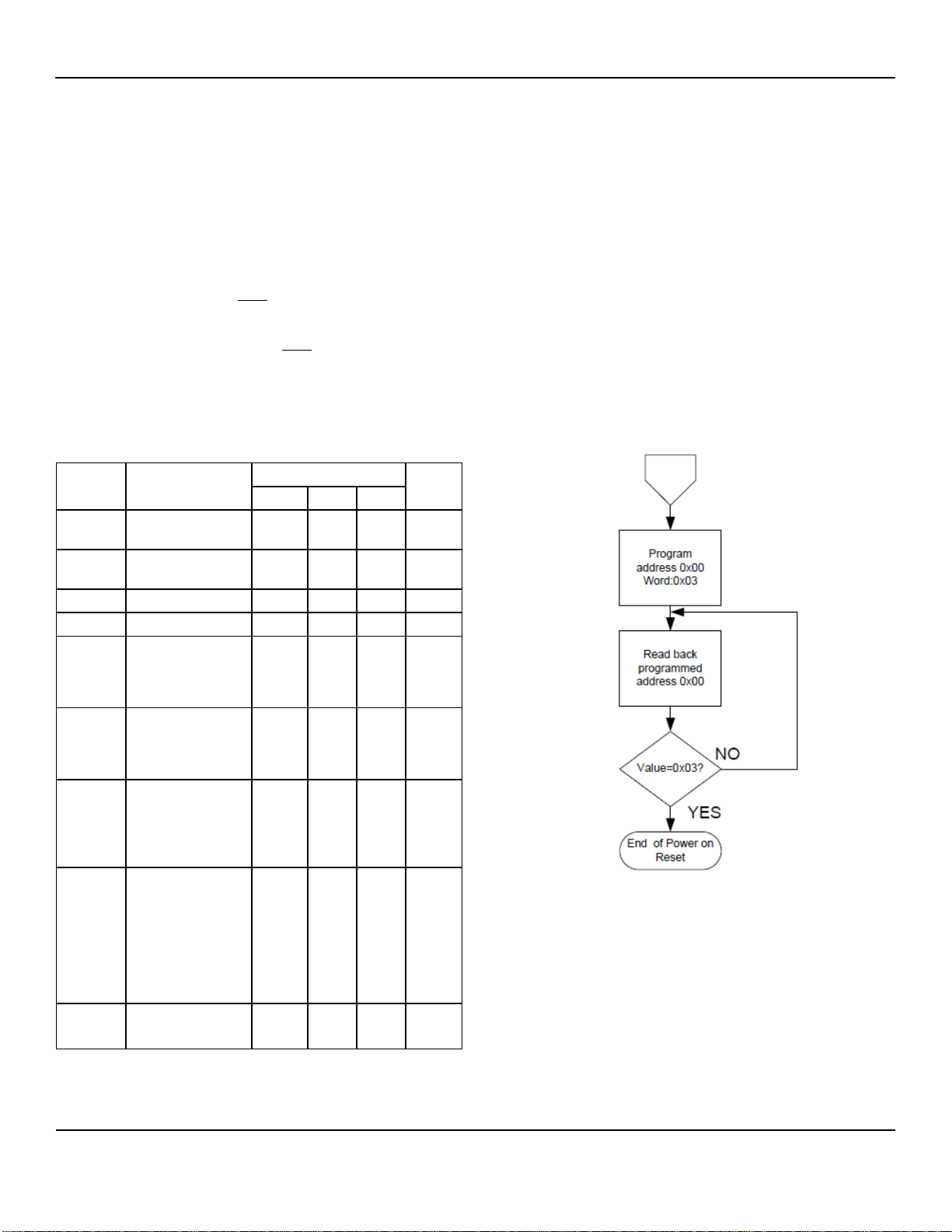
Power-on Reset
The power-on reset time (tPOR), given in Table 2, is defined
as the time from application of supply voltage to
completion of power on reset.
To determine when the chip has completed its power-on
without waiting for the worst-case time (maximum tPOR), do
the following:
•Write hex 03 (binary 00000011) to Register 0.
This puts the chip in Standby mode.
•Read Register 0. If the value read is binary
00000011, then exit; power-on is complete. If not,
go to previous step and repeat.
Because registers are initially in an unknown state after
power-on (exception: Mode[1:0] initializes to 00), always
enter a complete set of register values as the first
transaction, and always enter only nonzero values for N
and M.
Figure 5. Power-On Programming Flowchart
Micrel, Inc.
MICRF507
October 2, 2013
15
Revision 2.2
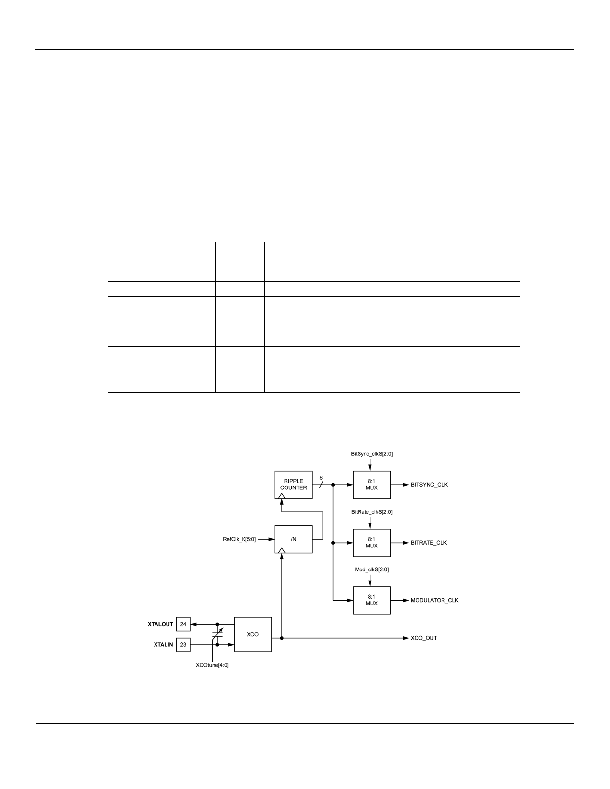
Clock Generation
The MICRF507’s crystal oscillator:
•Serves as the reference for the synthesizer that is
the carrier and local oscillator source.
•Is divided down to clock the switched-capacitor IF
filter.
•Is divided down to generate three other clocks: bit
rate clock, bit synchronization clock, and
modulator clock
Figure 6 shows the oscillator with its frequency-shifting
capacitor bank (controlled by the register field XCOtune)
and the frequency dividers that derive the latter three
clocks from its output. This division occurs in two stages.
First, the XCO output is divided by the 6-bit field Refclk_K,
which has allowable values between 1 and 63. Then, for
each of the three clocks, another field (BitSync_clkS,
BitRate_ClkS, and ModClkS, respectively) selects the
number of further divisions by 2. Complete relationships of
field values and resultant frequencies are given below for
each clock.
Field Name
Number
of bits
Location
of bits
Description
XCOtune 5 Reg9[4:0] Crystal oscillator trimming.
RefClk_K 6 Reg7[5:0] Reference clock divider.
BitRate_clkS 3 Reg6[0],
Reg7[7:6] Transmitter Bit rate clock setting. See Figure 9 and “Data
Interface and Bit Synchronization” section for more details.
Mod_clkS 3 Reg6[6:4] VCO Modulator clock setting, set the modulator clock to
either 8x or 16x the bit rate clock.
BitSync_clkS 3 Reg6[3:1]
Receiver Bit Synchronization clock setting, always set bit
synchronization clock to 16x the bit rate clock. See Figure 9
and “Data Interface and Bit Synchronization” section for more
details.
Table 3. Register Bit Fields for Clock Generation
Figure 6. MICRF507 Clock Sources

Micrel, Inc.
MICRF507
October 2, 2013
16
Revision 2.2
Crystal Oscillator (XCO)
The crystal oscillator’s role as the synthesizer reference
demands very good phase and frequency stability. As
shown in Figure 7, the external components required for
the oscillator are a crystal, connected between pins 23
and 24, and loading capacitors.
Pin 24
XtalOut Pin 23
XtalIn
C9
1.5pF C8
1.5pF
Y1
TN4-26011
Figure 7. Crystal Oscillator Circuit
The load capacitance CLseen between the crystal
terminals is:
pin
XCOtune
98
LCC
C
1
C
11
C ++
+
=
Where CXCOtune is the capacitance of the internal
adjustable capacitor bank, and Cpin is defined as the
internal chip capacitance when XCOtune bits are all
zeros, plus PCB stray capacitance across pins 23 and
24. The value of Cpin is about 6pF. The loading capacitor
values required depend on the total CLspecified for the
crystal for oscillation at the desired frequency.
It is possible to tune the crystal oscillator internally by
giving the 5-bit register field XCOtune a non-zero value,
which causes internal capacitors to be switched across
the crystal. As this capacitance increases, frequency
decreases. When XCOtune is set to its maximum value
of 31, approximately 4.5pF additional capacitance is
connected across the crystal pins.
The XCO tuning can be used to cancel crystal resonant
frequency error, both initial and with temperature. It can
be used in combination with the Frequency Error
Estimator (FEE). See “FEE” section.
The crystal used is a TN4-26011 from Toyocom.
Specification:
•Package TSX-10A,
•Nominal frequency 16.000000MHz
•Frequency tolerance ±10ppm
•Frequency stability ±9ppm, load capacitance
9pF
•Pulling sensitivity 15ppm/pF
To achieve 9pF load capacitance required to center
TN4-26011 at 16MHz, set the external capacitors to
1.5pF and XCOtune=16dec. Figure 8 shows the tuning
range for two different capacitor values, 1.5pF and zero
(external capacitors omitted). External capacitor values
will strongly affect the tuning range. Using 1.5pF with the
above crystal gives a tuning range that is approximately
symmetrical about the center frequency.
Figure 8. XCO Tuning with the XCOtune Field
The start-up time of the cystal oscillator, given in Table
4, is about a millisecond and increases with capacitance.
When the MICRF507’s main mode is switched from
Power down mode to Transmit mode via Standby mode,
or to Receive mode via Standby mode, only the XCO is
energized at first. Current consumption during this
prestart period is approximately 280μA (the same as for
Standby mode). After the XCO amplitude is sufficient to
trigger the M-counter and produce two pulses at its
output, the remaining circuits on the chip are powered
on.
XCOtune Start-up Time (µs)
0 590
1 590
2 700
4 700
8 810
16 1140
31 2050
Table 4. Typical Crystal Oscillator Start-up Time
with C8 = C9 = 1.5pF

Micrel, Inc.
MICRF507
October 2, 2013
17
Revision 2.2
An external reference clock, when used instead of a
crystal, should be applied to pin 24 (XTALOUT) with pin
23 (XTALIN) not connected. To maintain proper DC
biasing within the chip, use AC-coupling between the
external reference and the XTALOUT-pin.
BITSYNC_CLK (Receiver Bit Synchronization Clock)
The frequency of the bit synchronization clock
fBITSYNC_CLK, is a function of the crystal oscillator
frequency fXCO and the values of the register fields
Refclk_K and BitSync_clkS:
)-(7
XCO
KBITSYNC_CL
2Refclk_K f
f
kSBitSync_cl
×
=
The bit synchronizer uses a clock that needs to be
programmed to 16 times the actual bit rate. As an
example, a bit rate of 20kbps needs a bit synchronizer
clock with frequency of 320kHz. Refer to Figure 9 and
“Data Interface and Bit Synchronization” section for more
details.
BITRATE_CLK (Transmitter Bit Rate Clock)
The frequency fBITRATE_CLK of BITRATE_CLK is a function
of the crystal oscillator frequency fXCO and the values of
the register fields Refclk_K and BitRate_clkS:
kS)BitRate_cl-(7
XCO
KBITRATE_CL 2Refclk_Kf
f ×
=
In transmit mode, when Sync_en = 1, BITRATE_CLK
appears on the DATACLK pin. Its frequency is equal to
the bit rate. Example; a bit rate of 20 kbit/sec requires an
fBITRATE_CLK of 20kHz. Refer to Figure 9 and the “Data
Interface and Bit Synchronization” subsection for more
details.
MODULATOR_CLK (VCO Modulator Clock)
The frequency fMOD_CLK of MODULATOR_CLK is a
function of the crystal oscillator frequency fXCO and the
values of the register fields Refclk_K and Mod_clkS:
)-(7
XCO
MOD_CLK 2Refclk_Kf
f Mod_clkS
×
=
The modulator clock is used if VCO modulation method
is selected. Set the modulator clock frequency to either
8x or 16x the bit rate. See “VCO Modulation and the
Modulator” subsection for more information.
BitRate_clkS[2:0]
BitSync_clkS[2:0]
Mod_clkS[2:0]
Corresponding Clock
Frequency
(fXCO is crystal frequency)
000 fXCO/(128xRefClk_K)
001 fXCO/(64xRefClk_K)
010 fXCO/(32xRefClk_K)
011 fXCO/(16xRefClk_K)
100 fXCO/(8xRefClk_K)
101 fXCO/(4xRefClk_K)
110 fXCO/(2xRefClk_K) (*)
111 fXCO /RefClk_K (*)
(*) Can not be used as BitRate_clk.
Table 5. Generation of Bitrate_clk, BitSync_clk
and Mod_clk
Data Interface and Bit Synchronization
Transmitted and received data bits are coupled to the
MICRF507 serially through the Data Interface. This Data
Interface consists of the DATAIXO and DATACLK pins.
This is a separate interface from the Control Interface
(CS, IO, and SCLK), for which see Control (3-wire)
Interface.
Figure 9 shows the data interface circuitry aboard the
MICRF507. DATAIXO is an input during transmission,
whereas during reception a driver is enabled and it
becomes an output. DATACLK is always an output.
A rule that applies when using VCO modulation is: after
commanding the MICRF507 to enter transmit mode, the
microcontroller shall tri-state the driver connected to
DATAIXO to leave that pin floating until the
microcontroller begins sending data. See “Mode
Transitions” section for more details.
The data interface can be programmed for synchronous
and non-synchronous operation according to the setting
of the Sync_en bit; see Table 7.

Micrel, Inc.
MICRF507
October 2, 2013
18
Revision 2.2
Field Name
Number
of bits
Location
of bits Description Reference
Sync_en 1 Reg0[3] Synchronizer Mode bit Table 7
Table 6. Register Bit Fields for Data Interface and Bit Synchronization
Sync_en State Comments
0 RX: Bit
synchronization off Transparent reception of data
0 TX: DataClk pin off Transparent transmission of data
1 RX: Bit
synchronization on Bit clock is generated by transceiver
1 TX: DataClk pin on Bit clock is generated by transceiver
Table 7. Synchronizer Mode Bit
Figure 9. Data Interface and Synchronization
D Q
Bit
Sync
BITRATE_CLK
FROM
DEMOD
RECOVERED
CLOCK
RECEIVE
MODE
ENABLE
D Q
Sync_en
Sync_en = 0
Sync_en = 1
Sync_en = 0
Sync_en = 1
TRANSMIT
RECEIVE
19
18
DATAIXO
DATACLK
TO
TRANSMITTER
Filter &
data slicer
BITSYNC_CLK
TRANSMIT
DATA PATH
RECEIVE
DATA PATH
Micrel, Inc.
MICRF507
October 2, 2013
19
Revision 2.2
Mode Sync_en DATACLK DATAIXO
Direction Signal Direction Signal/Function
Transmit
0 Output 0 Input Modulates carrier directly
(asynchronously)
1 Output BitRate clock Input Sampled at rising edge of BitRate
clock; latched output modulates
carrier
Receive
0 Output 0 Output Raw output from demodulator
1 Output Clock recovered by bit
synchronizer
Output Filtered and latched demodulator
output; transitions occur at rising
edge of DATACLK
Table 8. Synchronizer Mode and Data Interface
In sync mode (Sync_en bit set to 1), the transmitted bit
stream is clocked with the precision of the MICRF507’s
crystal oscillator, which relaxes timing accuracy
requirements on the data source. During reception, the
synchronizer ensures that transitions of DATAIXO occur
only at rising edges of DATACLK, without edge jitter or
internal glitches. Receiver sensitivity values given in the
Electrical Characteristics table are measured with Sync_en
= 1; with Sync_en = 0, as much as 3-6 dB of sensitivity
could be lost.
Sync_en = 0
When Sync_en = 0, the input signal at DATAIXO
modulates the transmitter directly during transmission and
the output signal from DATAIXO is the raw demodulator
output. DATACLK remains fixed at a logic low level during
both transmission and reception.
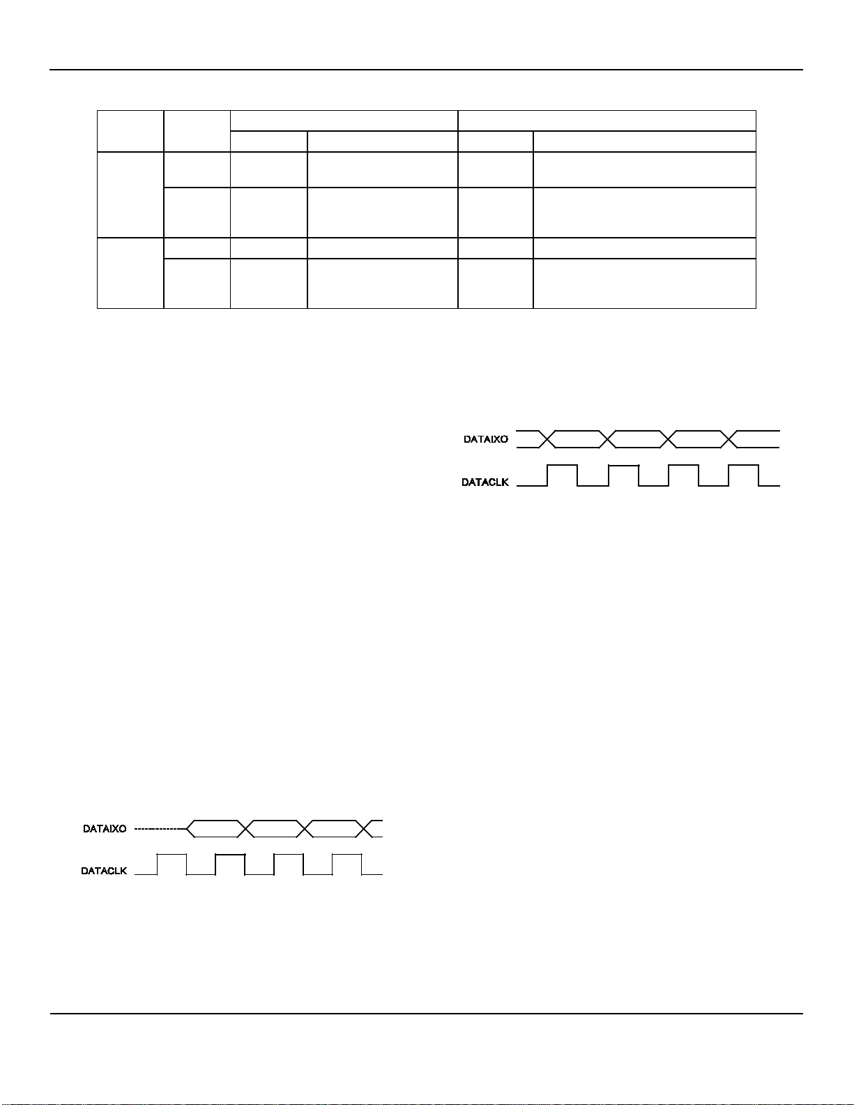
Sync_en = 1
During transmission when Sync_en = 1 the data bit stream
entering DATAIXO is buffered with a flip-flop strobed at the
rising edge of BITRATE_CLK, and the output of the flip-
flop modulates the transmitter. BITRATE_CLK is brought
out at the DATACLK output. Figure 10 shows the
relationship of DATACLK and DATAIXO transitions.
Figure 10. Data Interface in Transmit Mode
During reception, the bit synchronizer recovers the
received signal’s clock. This recovered clock strobes a flip-
flop that samples in mid-bit-period the demodulated and
filtered bit stream. The DATACLK output brings out the
recovered clock. DATAIXO (an output during reception)
brings out the synchronized data stream, which has its
transitions at rising edges of DATACLK. See Figure 11.
Figure 11. Data Interface in Receive Mode
By being in control of bit timing, the MICRF507 is
effectively the “master.” For maximum timing margin, the
microcontroller, as the “slave,” can present or sample
(during transmit and receive, respectively) each new bit at
the DATAIXO pin at falling edges of DATACLK.
Additional Considerations in the Use of Synchronizer
(Sync_en = 1)
Two clock signals, BITRATE_CLK and BITSYNC_CLK,
must be properly programmed when using the
synchronizer. BITRATE_CLK, used in transmission, must
be set to a frequency equal to the bit rate.
BITSYNC_CLK, used in reception, must have a frequency
16 times the bit rate. These frequencies are controlled by
the crystal oscillator frequency and the settings of register
fields, as described in the “Clock Generation” section. Bit
clocking of the incoming signal must agree with the
receiver’s local clocking within ±2.5% (easily met with 100
PPM or better crystals). For example, if fBITSYNC_CLK is
16x19.231kbps, the incoming bit rate can be between
0.975x19.231kbps to 1.025x19.231kbps.
All incoming messages must start with a 0101… preamble
so that the synchronizer can acquire the incoming clock. A
24-bit preamble is typically used; a minimum of 22 bits is
required.
Micrel, Inc.
MICRF507
October 2, 2013
20
Revision 2.2
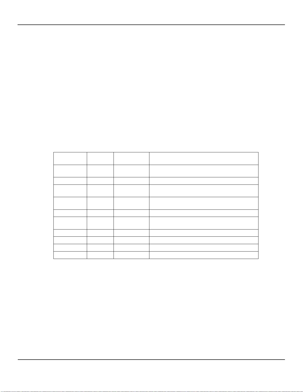
Frequency Synthesizer
The MICRF507 frequency synthesizer is an integer-N
phase-locked loop consisting of:
•a reference source, made of an M-divider
clocked by the crystal oscillator
•a voltage controlled oscillator (VCO)
•a programmable frequency divider made of an
N-divider, an A-divider, and a dual modulus
prescaler
•a phase/frequency detector
The loop filter is external for flexibility and can be a
simple passive circuit.
The phase/frequency detector compares the reference
frequency (from the M-divider) with the VCO output fed
through the programmable frequency divider. The
charge pump output of the phase/frequency detector,
after filtering, controls the VCO, closing the loop and forcing
the error between the reference frequency and the divided
VCO frequency to zero.
The block diagram, Figure 12, shows the basic elements and
arrangement of a PLL-based frequency synthesizer. The
MICRF507 has a dual modulus prescaler for increased
frequency resolution. In a dual modulus prescaler the main
divider is split into two parts, the main part N and an
additional divider A, where A < N. Both dividers are clocked
from the output of the dual-modulus prescaler, but only the
output of the N divider is fed into the phase detector. The
prescaler will first divide by 16. Both N and A count down
until A reaches zero, at which point the prescaler is switched
to a division ratio 16+1. At this point, the divider N has
completed A counts. Counting continues until N reaches
zero, which is an additional N-A counts. At this point, the
cycle repeats.
Field Name Number
of bits Location of bits
Description
M0 12 Reg13[3:0],
Reg14[7:0] M0 counter
A0 6 Reg10[5:0] A0 counter
N0 12 Reg11[3:0],
Reg12[7:0] N0 counter
M1 12 Reg18[3:0],
Reg19[7:0] M1 counter
A1 6 Reg15[5:0] A1 counter
N1 12 Reg16[3:0],
Reg17[7:0] N1 counter
CP_HI 1 Reg2[7] High charge pump current (1= 500μA, 0 = 125µA)
VCO_Freq 2 Reg3[1:0] Frequency setting of VCO (see Table 11)
VCO_IB 3 Reg3[4:2] VCO bias current setting (see Table 11)
LD_en 1 Reg1[2] Lock detect function on/off
Table 9. Register Bit Fields for Frequency Synthesizer
Table of contents


