Micrel KSZ8441FHL User manual
KSZ8441HL/FHL
IEEE 1588v2, Precision Time
Protocol-Enabled, 10/100Mbs,
Ethernet End-Point Connection
with 8- or 16-Bit Host Bus Interface
Revision 1.0
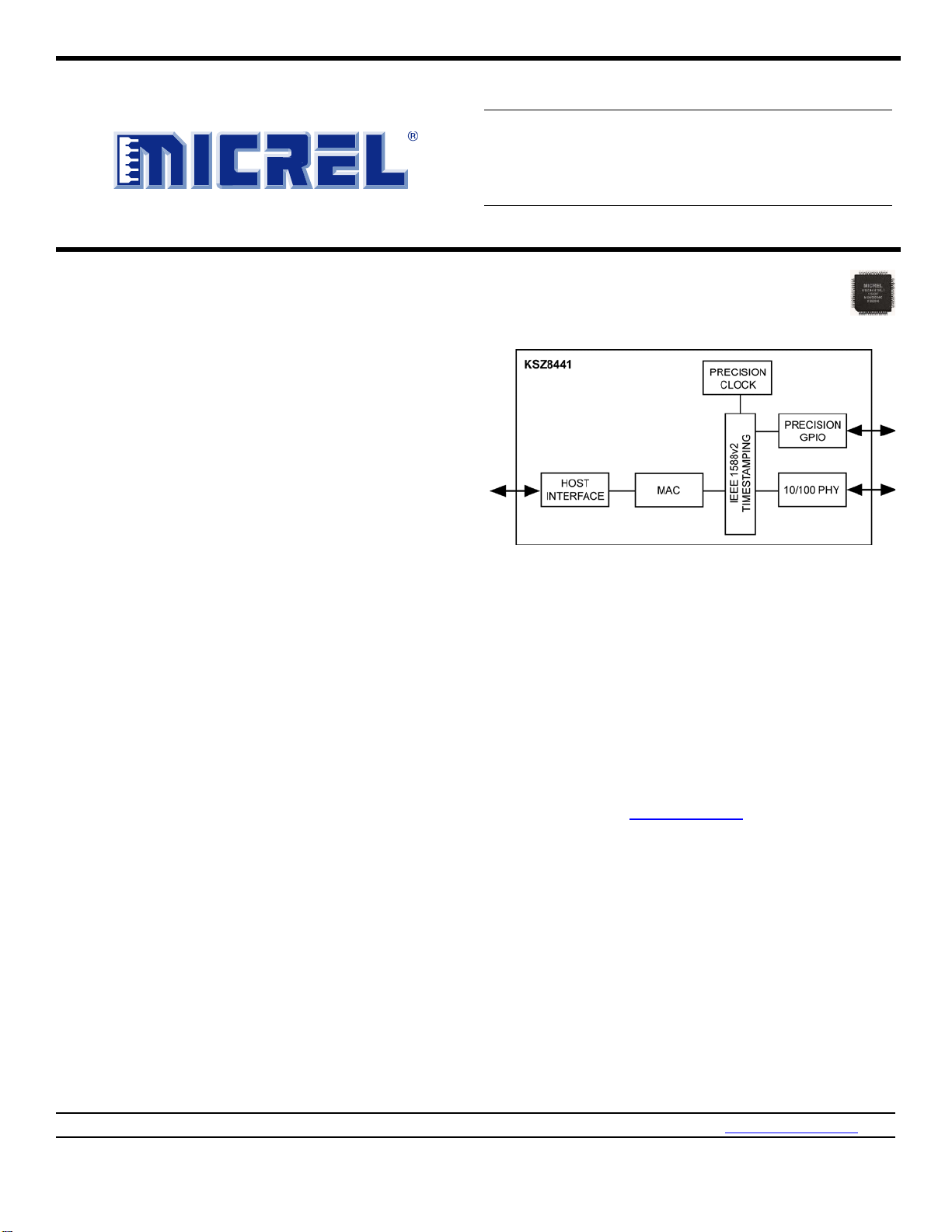
General Description
The KSZ8441 product is an IEEE 1588v2-enabled
Ethernet controller device with an internal MAC and PHY
that provides integrated communication and
synchronization for a range of industrial Ethernet
applications.
The KSZ8441 product enables end-point connection in a
centralized topology.
A flexible 8- or 16-bit general bus interface is provided for
interfacing to an external host processor.
The KSZ8441 devices incorporate the IEEE 1588v2
protocol. Sub-microsecond synchronization is available via
the use of hardware-based time stamping and transparent
clocks making it the ideal solution for time-synchronized
layer 2 communication in critical industrial applications.
Extensive general purpose input/output (GPIO) capabilities
are available to use with the IEEE 1588v2 PTP to
efficiently and accurately interface to locally-connected
devices.
Complementing the industry’s most integrated IEEE
1588v2 device is a precision timing protocol (PTP) v2
software stack that has been pre-qualified with the
KSZ84xx product family. The PTP stack has been
optimized around the KSZ84xx chip architecture, and is
available in source code format along with Micrel’s chip
driver.
ETHERSYNCH™
The KSZ8441 is built upon Micrel’s industry-leading
Ethernet technology, with features designed-to-offload
host processing and streamline overall design, including:
•1 integrated 10/100BASE-TX PHY transceiver,
featuring the industry’s lowest power consumption
•Flexible management options that support common
standard interfaces
A robust assortment of power management features
including energy-efficient Ethernet (EEE) have been
designed in to satisfy energy-efficient environments.
Datasheets and support documentation are available on
Micrel’s web site at: www.micrel.com.
ETHERSYNCH is a trademark of Micrel, Inc.
Magic Packet is a trademark of Advanced Micro Devices.
LinkMD is a registered trademark of Micrel, Inc.
Micrel Inc. • 2180 Fortune Drive • San Jose, CA 95131 • USA • tel +1 (408) 944-0800 • fax + 1 (408) 474-1000 • http://www.micrel.com
June 17, 2014 Revision -1.0
Micrel, Inc.
KSZ8441HL/FHL
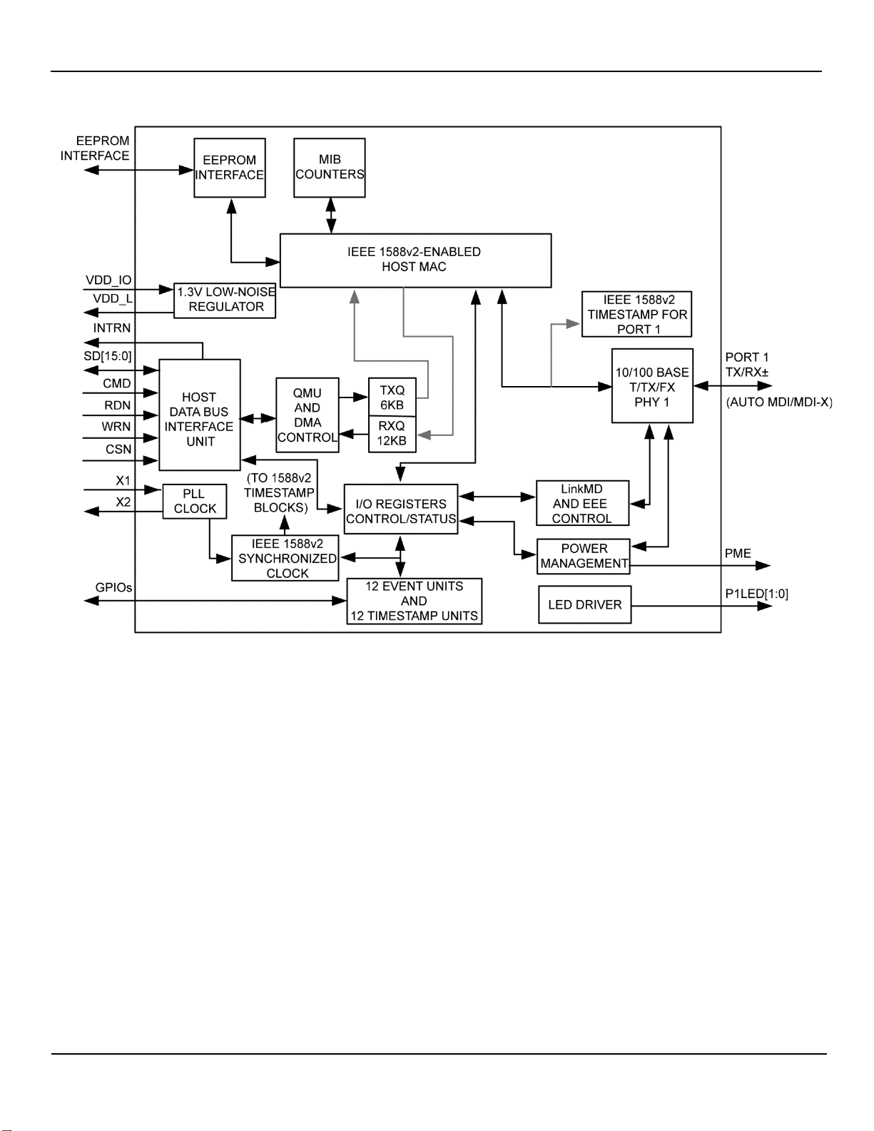
Functional Diagram
KSZ8441HL/FHL Functional Diagram
June 17, 2014 2 Revision 1.0

Micrel, Inc.
KSZ8441HL/FHL
Features
Management Capabilities
•Supports IP Header (IPV4)/TCP/UDP/ICMP checksum
generation and checking
•Supports IPV6 TCP/UDP/ICMP checksum generation
and checking
•Supports IEEE 802.3x full-duplex flow control and half-
duplex backpressure collision flow control
•MIB counters for fully-compliant statistics gathering -34
counters on the Ethernet Port, Port 1
•Loopback modes for remote failure diagnostics
Robust Ethernet PHY Port
•Integrated IEEE 802.3 / 802.3u-compliant Ethernet
transceiver supporting 10BASE-T and 100BASE-TX
•Copper- and fiber-mode support in the KSZ8441FHL
•Copper-mode support in the KSZ8441HL
•Auto-negotiation: 10/100 Mbps, full and half duplex
•Adaptive equalizer
•Baseline wander correction
•On-chip termination resistors and internal biasing for
differential pairs to reduce power
•HP Auto MDI/MDI-X crossover support eliminating the
need to differentiate between straight or crossover
cables in applications
Ethernet MAC
•Internal media access control (MAC) unit
•2000 byte jumbo packet support
•MAC filtering function to filter unknown unicast packets
•Port 1 MAC programmable as either end-to-end (E2E)
or peer-to-peer (P2P) transparent clock (TC) ports for
1588 support
Comprehensive Configuration Registers Access
•Complete register access via the parallel host interface
•Facility to load MAC address from EEPROM at power-
up and reset time
•I/O pin strapping facility to set certain register bits from
I/O pin states at Reset time
•Control registers configurable on-the-fly
IEEE 1588V2 PTP and Clock Synchronization
•Fully compliant with the appropriate IEEE 1588v2
precision time protocol
•One-step or two-step transparent clock (TC) timing
corrections
•End-to-end (E2E) or peer-to-peer (P2P) transparent
clock (TC)
•Grandmaster, master, slave, ordinary clock (OC)
Support
•IEEE1588v2 PTP multicast and unicast frame support
•Transports of PTP over IPv4/IPv6 UDP and IEEE 802.3
Ethernet
•Delay request-response and peer delay mechanism
•Ingress/egress packet timestamp capture/recording and
checksum update
•Correction field update with residence time and link
delay
•IEEE1588v2 PTP packet filtering unit to reduce host
processor overhead
•A 64-bit adjustable system precision clock
•Twelve trigger output units and twelve timestamp input
units available for flexible IEEE1588v2 control of seven
programmable GPIO[6:0] pins synchronized to the
precision time clock
•GPIO pin usage for 1 PPS generation, frequency
generation, control bit streams, event monitoring,
precision pulse generation, complex waveform
generation
Host Interface
•Selectable 8- or 16-bit wide interface
•Supports big- and little-endian processors
•Indirect data bus for data, address, and byte enable to
access any I/O registers and RX/TX FIFO buffers
•Large internal memory with 12KB for RX FIFO and 6KB
for TX FIFO.
•Programmable low, high, and overrun water mark for
flow control in RX FIFO
•Efficient architecture design with configurable host
interrupt schemes to minimize host CPU overhead and
utilization
•Queue management unit (QMU) supervises data
transfers across this interface
June 17, 2014 3 Revision 1.0

Micrel, Inc.
KSZ8441HL/FHL
Power and Power Management
•Single 3.3V power supply with optional 1.8V, 2.5V, or
3.3V VDD I/O.
•Integrated low voltage (~1.3V) low-noise regulator
(LDO) output for digital and analog core power
•Supports IEEE P802.3az energy efficient Ethernet
(EEE) to reduce power consumption in transceiver in
LPI state
•Full-chip hardware or software power down (all registers
value are not saved and strap-in value will re-strap after
release the power down)
•Energy detect power-down (EDPD), which disables the
PHY transceiver when cables are removed
•Wake On LAN supported with Magic Packet™ , link
state, and configurable wake-up packet control
•Dynamic clock tree control to reduce clocking in areas
not in use
•Power consumption less than 0.5W
Additional Features
•Single 25MHz ±50 ppm reference clock requirement
•Comprehensive programmable two LED indicators
support for link, activity, full/half duplex and 10/100
speed
•LED pins directly controllable
•Industrial temperature range: –40°C to +85°C
•64-pin, 10mm × 10mm, lead-free (RoHS) LQFP
package
•0.11µm technology for lower power consumption
Applications
•Industrial Ethernet applications that employ IEEE 802.3-
compliant MACs. (Ethernet/IP, Profinet, MODBUS TCP,
etc.)
•Real-time Ethernet networks requiring sub-microsecond
synchronization over standard Ethernet
•IEC 61850 networks supporting power substation
automation
•Networked measurement and control systems
•Industrial automation and motion control systems
•Test and measurement equipment
Ordering Information
Part Number
Temperature Range
Package
Lead Finish
Description
KSZ8441HLI –40°C to +85°C 64-Pin LQFP Pb-Free Industrial Temperature Device with Generic Host
Interface
KSZ8441FHLI –40°C to +85°C 64-Pin LQFP Pb-Free Industrial Temperature Device with Generic Host
Interface and Fiber (100BASE-FX) support
KSZ8441HLI-EVAL Evaluation Board with KSZ8441HLI. Also supports the KSZ8441FHLI.
Revision History
Revision
Date
Summary of Changes
1.0 6/9/2014 Initial release of KSZ8441HL/FHL product datasheet.
June 17, 2014 4 Revision 1.0

Micrel, Inc.
KSZ8441HL/FHL
Contents
Acronyms ..............................................................................................................................................................................15
Pin Configuration...................................................................................................................................................................17
Pin Description......................................................................................................................................................................18
Strapping Options .................................................................................................................................................................24
Functional Description...........................................................................................................................................................25
Phy (Physical) Block .............................................................................................................................................................26
100BASE-TX Transmit......................................................................................................................................................26
100BASE-TX Receive.......................................................................................................................................................26
Scrambler/De-scrambler (100BASE-TX only)...................................................................................................................26
PLL Clock Synthesizer (Recovery)....................................................................................................................................26
100BASE-FX Operation ....................................................................................................................................................26
100BASE-FX Signal Detection..........................................................................................................................................27
100BASE-FX Far-End Fault..................................................................................................................................................27
10BASE-T Transmit...........................................................................................................................................................27
10BASE-T Receive............................................................................................................................................................27
MDI/MDI-X Auto Crossover...............................................................................................................................................27
Straight Cable................................................................................................................................................................28
Crossover Cable............................................................................................................................................................28
Auto-Negotiation ...................................................................................................................................................................29
LinkMD®Cable Diagnostics..................................................................................................................................................30
Access............................................................................................................................................................................30
Usage.............................................................................................................................................................................30
On-chip Termination Resistors..........................................................................................................................................30
Loopback Support.................................................................................................................................................................31
Near-End (Remote) Loopback.......................................................................................................................................31
Far-End (Local) Loopback .............................................................................................................................................31
MAC (Media Access Controller) Block..................................................................................................................................32
MAC Operation..................................................................................................................................................................32
Inter-Packet Gap (IPG)......................................................................................................................................................32
Back-Off Algorithm ............................................................................................................................................................32
Late Collision.....................................................................................................................................................................32
Legal Packet Size..............................................................................................................................................................32
Flow Control ......................................................................................................................................................................32
Half-Duplex Backpressure.................................................................................................................................................32
Address Filtering Function ....................................................................................................................................................33
Queue Management Unit (QMU)..........................................................................................................................................34
Transmit Queue (TXQ) Frame Format..............................................................................................................................34
Frame Transmitting Path Operation in TXQ......................................................................................................................35
Driver Routine for Transmitting Packets from Host Processor to KSZ8441 .....................................................................36
Receive Queue (RXQ) Frame Format...............................................................................................................................37
Frame Receiving Path Operation in RXQ.........................................................................................................................37
Driver Routine for Receiving Packets from the KSZ8441 to the Host Processor.............................................................38
IEEE 1588 Precision Time Protocol (PTP) Block..................................................................................................................40
IEEE 1588 PTP Clock Types................................................................................................................................................41
IEEE 1588 PTP One-Step or Two-Step Clock Operation.....................................................................................................41
One-Step Clock Operation:...............................................................................................................................................41
Two-Step Clock Operation:...............................................................................................................................................41
IEEE 1588 PTP Best Master Clock Selection.......................................................................................................................41
IEEE 1588 PTP System Time Clock.....................................................................................................................................42
Updating the System time Clock....................................................................................................................................43
Directly Setting or Reading the Time.................................................................................................................................43
Step Time Adjustment.......................................................................................................................................................43
Continuous Time Adjustment............................................................................................................................................43
Temporary Time Adjustment.............................................................................................................................................43
PTP Clock Initialization......................................................................................................................................................43
IEEE 1588 PTP Message Processing ..................................................................................................................................45
June 17, 2014 5 Revision 1.0

Micrel, Inc.
KSZ8441HL/FHL
IEEE 1588 PTP Ingress Packet Processing......................................................................................................................45
IEEE 1588 PTP Egress Packet Processing......................................................................................................................45
IEEE 1588 PTP Event Triggering and Timestamping...........................................................................................................46
IEEE 1588 PTP Trigger Outputs.......................................................................................................................................46
IEEE 1588 PTP Event Timestamp Input...........................................................................................................................46
IEEE 1588 PTP Event Interrupts.......................................................................................................................................47
IEEE 1588 GPIO ...............................................................................................................................................................47
General Purpose and IEEE 1588 Input/Output (GPIO)........................................................................................................48
Overview............................................................................................................................................................................48
GPIO Pin Functionality Control .........................................................................................................................................48
GPIO Pin Control Register Layout ....................................................................................................................................49
GPIO Trigger Output Units and Timestamp Input Unit Interrupts .....................................................................................52
Using the GPIO Pins with the Trigger Output Units..........................................................................................................53
Creating a Low-Going Pulse at a Specific Time............................................................................................................53
Creating a High-Going Pulse at a Specific Time...........................................................................................................53
Creating a Free Running Clock Source.........................................................................................................................54
Creating Finite Length Periodic Bit Streams at a Specific Time....................................................................................55
Creating Finite Length Non-Uniform Bit Streams at a Specific Time................................................................................55
Creating Complex Waveforms at a Specific Time.............................................................................................................56
Using the GPIO Pins with the Timestamp Input Units.......................................................................................................57
Timestamping an Incoming Low-Going Edge................................................................................................................57
Timestamping an Incoming High-Going Edge...............................................................................................................58
Timestamping an Incoming Low-Going Pulse or High Going Pulse..............................................................................58
Device Clocks........................................................................................................................................................................59
GPIO and IEEE 1588 Related Clocking................................................................................................................................59
Power....................................................................................................................................................................................60
Internal low Voltage LDO Regulator..................................................................................................................................61
Power Management..............................................................................................................................................................62
Normal Operation Mode....................................................................................................................................................62
Energy Detect Mode..........................................................................................................................................................62
Global Soft Power Down Mode.........................................................................................................................................62
Transmit Direction Control for MII Mode ...........................................................................................................................64
Receive Direction Control for MII Mode.........................................................................................................................64
Registers Associated with EEE .....................................................................................................................................64
Wake On LAN....................................................................................................................................................................64
Detection of Energy .......................................................................................................................................................64
Detection of Link-up.......................................................................................................................................................64
Wake-Up Packet............................................................................................................................................................65
Magic Packet™..............................................................................................................................................................65
Interrupt Generation on Power Management Related Events ..........................................................................................65
Bus Interface Unit (BIU) / Host Interface...........................................................................................................................66
Supported Transfers..........................................................................................................................................................66
Physical Data Bus Size .....................................................................................................................................................66
Little and Big Endian Support............................................................................................................................................67
Asynchronous Interface.....................................................................................................................................................67
BIU Summary.................................................................................................................................................................68
Serial EEPROM Interface..................................................................................................................................................69
Device Registers...................................................................................................................................................................70
Register Map of CPU Accessible I/O Registers....................................................................................................................72
I/O Registers......................................................................................................................................................................72
Internal I/O Register Space Mapping for General Control and Configuration (0x000 – 0x0FF)...........................................73
Internal I/O Register Space Mapping for Host Interface Unit (0x100 – 0x16F)....................................................................76
Internal I/O Register Space Mapping for the QMU (0x170 – 0x1FF)....................................................................................78
Internal I/O Register Space Mapping for PTP Trigger Output (12 Units, 0x200 – 0x3FF) ...................................................80
Internal I/O Register Space Mapping for PTP Event Timestamp Input (12 Units, 0x400 – 0x5FF) .....................................88
Internal I/O Register Space Mapping for PTP 1588 Clock and Global Control (0x600 – 0x7FF).........................................98
Register Bit Definitions........................................................................................................................................................100
June 17, 2014 6 Revision 1.0

Micrel, Inc.
KSZ8441HL/FHL
Internal I/O Registers Space Mapping for General Control and Configuration (0x000 – 0x0FF) 100
Chip ID and Enable Register (0x000 – 0x001): CIDER......................................................................................................100
General Global Control Register 1 (0x002 - 0x003): GGCR1.............................................................................................101
0x004 – 0x00D: Reserved...................................................................................................................................................101
General Global Control Register 7 (0x00E – 0x00F): GGCR7...........................................................................................102
MAC Address Register 1 (0x010 – 0x011): MACAR1 ........................................................................................................102
MAC Address Register 2 (0x012 – 0x013): MACAR2 ........................................................................................................102
MAC Address Register 3 (0x014 – 0x015): MACAR3 ........................................................................................................102
0x016 – 0x025: Reserved...................................................................................................................................................103
Indirect Access Data Register 1 (0x026 – 0x027): IADR1..................................................................................................103
0x028– 0x02B: Reserved....................................................................................................................................................103
Indirect Access Data Register 4 (0x02C – 0x02D): IADR4.................................................................................................103
Indirect Access Data Register 5 (0x02E – 0x02F): IADR5 .................................................................................................103
Indirect Access Control Register (0x030 – 0x031): IACR...................................................................................................103
Power Management Control and Wake-up Event Status (0x032 – 0x033): PMCTRL.......................................................104
Power Management Event Enable Register (0x034 – 0x035): PMEE................................................................................104
Go Sleep Time Register (0x036 – 0x037): GST.................................................................................................................105
Clock Tree Power Down Control Register (0x038 – 0x039): CTPDC.................................................................................105
0x03A – 0x04B: Reserved ..................................................................................................................................................105
PHY 1 and MII Basic Control Register (0x04C – 0x04D): P1MBCR ..................................................................................106
PHY 1 and MII Basic Status Register (0x04E – 0x04F): P1MBSR.....................................................................................108
PHY 1 PHYID Low Register (0x050 – 0x051): PHY1ILR ...................................................................................................109
PHY 1 PHYID High Register (0x052 – 0x053): PHY1IHR..................................................................................................109
PHY 1 Auto-Negotiation Advertisement Register (0x054 – 0x055): P1ANAR....................................................................109
PHY 1 Auto-Negotiation Link Partner Ability Register (0x056 – 0x057): P1ANLPR...........................................................110
0x058 – 0x065: Reserved...................................................................................................................................................110
PHY 1 Special Control and Status Register (0x066 – 0x067): P1PHYCTRL.....................................................................111
0x068 – 0x06B: Reserved...................................................................................................................................................111
Port 1 Control Register 1 (0x06C – 0x06D): P1CR1...........................................................................................................111
0x06E – 0x07B: Reserved ..................................................................................................................................................111
Port 1 PHY Special Control/Status, LinkMD®(0x07C – 0x07D): P1SCSLMD....................................................................112
Port 1 Control Register 4 (0x07E – 0x07F): P1CR4...........................................................................................................113
0x082 – 0x0D5: Reserved...................................................................................................................................................115
Input and Output Multiplex Selection Register (0x0D6 – 0x0D7): IOMXSEL .....................................................................115
Configuration Status and Serial Bus Mode Register (0x0D8 – 0x0D9): CFGR..................................................................116
0x0DA – 0x0DB: Reserved.................................................................................................................................................116
Port 1 Auto-Negotiation Next Page Transmit Register (0x0DC – 0x0DD): P1ANPT..........................................................116
Port 1 Auto-Negotiation Link Partner Received Next Page Register (0x0DE – 0x0DF): P1ALPRNP................................117
Port 1 EEE and Link Partner Advertisement Register (0x0E0 – 0x0E1): P1EEEA............................................................118
Port 1 EEE Wake Error Count Register (0x0E2 – 0x0E3): P1EEEWEC............................................................................119
Port 1 EEE Control/Status and Auto-Negotiation Expansion Register (0x0E4 – 0x0E5): P1EEECS ................................119
Port 1 LPI Recovery Time Counter Register (0x0E6): P1LPIRTC......................................................................................120
Buffer Load to LPI Control 1 Register (0x0E7): BL2LPIC1.................................................................................................120
0x0E8 – 0x0F1: Reserved...................................................................................................................................................120
PCS EEE Control Register (0x0F2 – 0xF3): PCSEEEC.....................................................................................................121
Empty TXQ to LPI Wait Time Control Register (0x0F4 – 0x0F5): ETLWTC......................................................................121
Buffer Load to LPI Control 2 Register (0x0F6 – 0x0F7): BL2LPIC2...................................................................................121
0x0F8 – 0x0FF: Reserved...................................................................................................................................................121
Internal I/O Register Space Mapping for Interrupts, BIU, and Global Reset (0x100 – 0x1FF)...........................................122
0x100 – 0x107: Reserved...................................................................................................................................................122
Chip Configuration Register (0x108 – 0x109): CCR...........................................................................................................122
0x10A – 0x10F: Reserved...................................................................................................................................................122
Host MAC Address Registers: MARL, MARM and MARH .................................................................................................123
Host MAC Address Register Low (0x110 – 0x111): MARL................................................................................................123
Host MAC Address Register Middle (0x112 – 0x113): MARM...........................................................................................123
Host MAC Address Register High (0x114 – 0x115): MARH...............................................................................................123
0x116 – 0x121: Reserved...................................................................................................................................................123
June 17, 2014 7 Revision 1.0

Micrel, Inc.
KSZ8441HL/FHL
EEPROM Control Register (0x122 – 0x123): EEPCR........................................................................................................124
Memory BIST Info Register (0x124 – 0x125): MBIR...........................................................................................................124
Global Reset Register (0x126 – 0x127): GRR....................................................................................................................125
0x128 – 0x129: Reserved...................................................................................................................................................125
Wake-Up Frame Control Register (0x12A – 0x12B): WFCR..............................................................................................125
0x12C – 0x12F: Reserved ..................................................................................................................................................126
Wake-Up Frame 0 CRC0 Register (0x130 – 0x131): WF0CRC0.......................................................................................126
Wake-Up Frame 0 CRC1 Register (0x132 – 0x133): WF0CRC1.......................................................................................126
Wake-Up Frame 0 Byte Mask 0 Register (0x134 – 0x135): WF0BM0...............................................................................127
Wake-Up Frame 0 Byte Mask 1 Register (0x136 – 0x137): WF0BM1...............................................................................127
Wake-Up Frame 0 Byte Mask 2 Register (0x138 – 0x139): WF0BM2...............................................................................127
Wake-Up Frame 0 Byte Mask 3 Register (0x13A – 0x13B): WF0BM3 ..............................................................................127
0x13C – 0x13F: Reserved ..................................................................................................................................................127
Wake-Up Frame 1 CRC0 Register (0x140 – 0x141): WF1CRC0.......................................................................................127
Wake-Up Frame 1 CRC1 Register (0x142 – 0x143): WF1CRC1.......................................................................................128
Wake-Up Frame 1 Byte Mask 0 Register (0x144 – 0x145): WF1BM0...............................................................................128
Wake-Up Frame 1 Byte Mask 1 Register (0x146 – 0x147): WF1BM1...............................................................................128
Wake-Up Frame 1 Byte Mask 2 Register (0x148 – 0x149): WF1BM2...............................................................................128
Wake-Up Frame 1 Byte Mask 3 Register (0x14A – 0x14B): WF1BM3 ..............................................................................128
0x14C – 0x14F: Reserved ..................................................................................................................................................128
Wake-Up Frame 2 CRC0 Register (0x150 – 0x151): WF2CRC0.......................................................................................129
Wake-Up Frame 2 CRC1 Register (0x152 – 0x153): WF2CRC1.......................................................................................129
Wake-Up Frame 2 Byte Mask 0 Register (0x154 – 0x155): WF2BM0...............................................................................129
Wake-Up Frame 2 Byte Mask 1 Register (0x156 – 0x157): WF2BM1...............................................................................129
Wake-Up Frame 2 Byte Mask 2 Register (0x158 – 0x159): WF2BM2...............................................................................129
Wake-Up Frame 2 Byte Mask 3 Register (0x15A – 0x15B): WF2BM3 ..............................................................................130
0x15C – 0x15F: Reserved ..................................................................................................................................................130
Wake-Up Frame 3 CRC0 Register (0x160 – 0x161): WF3CRC0.......................................................................................130
Wake-Up Frame 3 CRC1 Register (0x162 – 0x163): WF3CRC1.......................................................................................130
Wake-Up Frame 3 Byte Mask 0 Register (0x164 – 0x165): WF3BM0...............................................................................130
Wake-Up Frame 3 Byte Mask 1 Register (0x166 – 0x167): WF3BM1...............................................................................130
Wake-Up Frame 3 Byte Mask 2 Register (0x168 – 0x169): WF3BM2...............................................................................131
Wake-Up Frame 3 Byte Mask 3 Register (0x16A – 0x16B): WF3BM3 ..............................................................................131
0x16C – 0x16F: Reserved ..................................................................................................................................................131
Internal I/O Registers Space Mapping for the Queue Management Unit (QMU) (0x170 – 0x1FF)....................................132
Transmit Control Register (0x170 – 0x171): TXCR............................................................................................................132
Transmit Status Register (0x172 – 0x173): TXSR..............................................................................................................133
Receive Control Register 1 (0x174 – 0x175): RXCR1........................................................................................................133
Receive Control Register 2 (0x176 – 0x177): RXCR2........................................................................................................134
TXQ Memory Information Register (0x178 – 0x179): TXMIR.............................................................................................135
0x17A – 0x17B: Reserved ..................................................................................................................................................135
Receive Frame Header Status Register (0x17C – 0x17D): RXFHSR................................................................................135
Receive Frame Header Byte Count Register (0x17E – 0x17F): RXFHBCR ......................................................................136
TXQ Command Register (0x180 – 0x181): TXQCR...........................................................................................................136
RXQ Command Register (0x182 – 0x183): RXQCR..........................................................................................................137
TX Frame Data Pointer Register (0x184 – 0x185): TXFDPR.............................................................................................138
RX Frame Data Pointer Register (0x186 – 0x187): RXFDPR............................................................................................138
0x188 – 0x18B: Reserved...................................................................................................................................................138
RX Duration Timer Threshold Register (0x18C – 0x18D): RXDTTR..................................................................................139
RX Data Byte Count Threshold Register (0x18E – 0x18F): RXDBCTR.............................................................................139
Internal I/O Registers Space Mapping for Interrupt Registers (0x190 – 0x193).................................................................139
Interrupt Enable Register (0x190 – 0x191): IER.................................................................................................................140
Interrupt Status Register (0x192 – 0x193): ISR..................................................................................................................141
0x194 – 0x19B: Reserved...................................................................................................................................................142
Internal I/O Registers Space Mapping for the Queue Management Unit (QMU) (0x19C – 0x1B9)...................................143
RX Frame Count & Threshold Register (0x19C – 0x19D): RXFCTR.................................................................................143
TX Next Total Frames Size Register (0x19E – 0x19F): TXNTFSR....................................................................................143
June 17, 2014 8 Revision 1.0

Micrel, Inc.
KSZ8441HL/FHL
MAC Address Hash Table Register 0 (0x1A0 – 0x1A1): MAHTR0....................................................................................143
MAC Address Hash Table Register 1 (0x1A2 – 0x1A3): MAHTR1....................................................................................143
MAC Address Hash Table Register 2 (0x1A4 – 0x1A5): MAHTR2....................................................................................144
MAC Address Hash Table Register 3 (0x1A6 – 0x1A7): MAHTR3....................................................................................144
0x1A8 – 0x1AF: Reserved..................................................................................................................................................144
Flow Control Low Water Mark Register (0x1B0 – 0x1B1): FCLWR ...................................................................................144
Flow Control High Water Mark Register (0x1B2 – 0x1B3): FCHWR..................................................................................144
Flow Control Overrun Water Mark Register (0x1B4 – 0x1B5): FCOWR............................................................................144
0x1B6 – 0x1B7: Reserved ..................................................................................................................................................145
RX Frame Count Register (0x1B8 – 0x1B9): RXFC...........................................................................................................145
0x1BA – 0x1FF: Reserved..................................................................................................................................................145
Internal I/O Registers Space Mapping for Trigger Output Units (12 Units, 0x200 – 0x3FF) ..............................................145
Trigger Error Register (0x200 – 0x201): TRIG_ERR..........................................................................................................145
Trigger Active Register (0x202 – 0x203): TRIG_ACTIVE...................................................................................................145
Trigger Done Register (0x204 – 0x205): TRIG_DONE ......................................................................................................146
Trigger Enable Register (0x206 – 0x207): TRIG_EN .........................................................................................................146
Trigger Software Reset Register (0x208 – 0x209): TRIG_SW_RST..................................................................................146
Trigger Output Unit 12 Output PPS Pulse Width Register (0x20A – 0x20B): TRIG12_PPS_WIDTH................................146
0x20C – 0x21F: Reserved ..................................................................................................................................................147
Trigger Output Unit 1 Target Time in Nanoseconds Low-Word Register (0x220 – 0x221): TRIG1_TGT_NSL.................147
Trigger Output Unit 1 Target Time in Nanoseconds High-Word Register (0x222 – 0x223): TRIG1_TGT_NSH ...............147
Trigger Output Unit 1 Target Time in Seconds Low-Word Register (0x224 – 0x225): TRIG1_TGT_SL............................147
Trigger Output Unit 1 Target Time in Seconds High-word Register (0x226 – 0x227): TRIG1_TGT_SH...........................147
Trigger Output Unit 1 Configuration and Control Register 1 (0x228 – 0x229): TRIG1_CFG_1.........................................148
Trigger Output Unit 1 Configuration and Control Register 2 (0x22A – 0x22B): TRIG1_CFG_2 ........................................149
Trigger Output Unit 1 Configuration and Control Register 3 (0x22C – 0x22D): TRIG1_CFG_3........................................149
Trigger Output Unit 1 Configuration and Control Register 4 (0x22E – 0x22F): TRIG1_CFG_4.........................................149
Trigger Output Unit 1 Configuration and Control Register 5 (0x230 – 0x231): TRIG1_CFG_5.........................................150
Trigger Output Unit 1 Configuration and Control Register 6 (0x232 – 0x233): TRIG1_CFG_6.........................................150
Trigger Output Unit 1 Configuration and Control Register 7 (0x234 – 0x235): TRIG1_CFG_7.........................................150
Trigger Output Unit 1 Configuration and Control Register 8 (0x236 – 0x237): TRIG1_CFG_8.........................................150
0x238 – 0x23F: Reserved...................................................................................................................................................150
Trigger Output Unit 2 Target Time and Output Configuration/Control Registers (0x240 – 0x257) ....................................151
Trigger Output Unit 2 Configuration and Control Register 1 (0x248 – 0x249): TRIG2_CFG_1.........................................151
0x258 – 0x25F: Reserved...................................................................................................................................................151
Trigger Output Unit 3 Target Time and Output Configuration/Control Registers (0x260 – 0x277) ....................................151
0x278 – 0x27F: Reserved...................................................................................................................................................151
Trigger Output Unit 4 Target Time and Output Configuration/Control Registers (0x280 – 0x297) ....................................151
0x298 – 0x29F: Reserved...................................................................................................................................................151
Trigger Output Unit 5 Target Time and Output Configuration/Control Registers (0x2A0 – 0x2B7)....................................151
0x2B8 – 0x2BF: Reserved..................................................................................................................................................151
Trigger Output Unit 6 Target Time and Output Configuration/Control Registers (0x2C0 – 0x2D7)...................................151
0x2D8 – 0x2DF: Reserved..................................................................................................................................................151
Trigger Output Unit 7 Target Time and Output Configuration/Control Registers (0x2E0 – 0x2F7)....................................151
0x2F8 – 0x2FF: Reserved...................................................................................................................................................152
Trigger Output Unit 8 Target Time and Output Configuration/Control Registers (0x300 – 0x317) ....................................152
0x318 – 0x31F: Reserved...................................................................................................................................................152
Trigger Output Unit 9 Target Time and Output Configuration/Control Registers (0x320 – 0x337) ....................................152
0x338 – 0x33F: Reserved...................................................................................................................................................152
Trigger Output Unit 10 Target Time and Output Configuration/Control Registers (0x340 – 0x357) ..................................152
0x358 – 0x35F: Reserved...................................................................................................................................................152
Trigger Output Unit 11 Target Time and Output Configuration/Control Registers (0x360 – 0x377) ..................................152
0x378 – 0x37F: Reserved...................................................................................................................................................152
Trigger Output Unit 12 Target Time and Output Configuration/Control Registers (0x380 – 0x397) ..................................152
0x398 – 0x3FF: Reserved...................................................................................................................................................152
Internal I/O Registers Space Mapping for PTP Timestamp Inputs (12 Units, 0x400 – 0x5FF)..........................................152
Timestamp Ready Register (0x400 – 0x401): TS_RDY.....................................................................................................153
June 17, 2014 9 Revision 1.0

Micrel, Inc.
KSZ8441HL/FHL
Timestamp Enable Register (0x402 – 0x403): TS_EN.......................................................................................................153
Timestamp Software Reset Register (0x404 – 0x405): TS_SW_RST ...............................................................................153
0x406 – 0x41F: Reserved...................................................................................................................................................153
Timestamp Unit 1 Status Register (0x420 – 0x421): TS1_STATUS..................................................................................154
Timestamp Unit 1 Configuration and Control Register (0x422 – 0x423): TS1_CFG..........................................................154
Timestamp Unit 1 Input 1st Sample Time in Nanoseconds Low-word Register (0x424 – 0x425): TS1_SMPL1_NSL......155
Timestamp Unit 1 Input 1st Sample Time in Nanoseconds High-word Register (0x426 – 0x427): TS1_SMPL1_NSH ....155
Timestamp Unit 1 Input 1st Sample Time in Seconds Low-word Register (0x428 – 0x429): TS1_SMPL1_SL ................155
Timestamp Unit 1 Input 1st Sample Time in Seconds High-word Register (0x42A – 0x42B): TS1_SMPL1_SH..............155
Timestamp Unit 1 Input 1st Sample Time in Sub-Nanoseconds Register (0x42C – 0x42D): TS1_SMPL1_SUB_NS......156
0x42E – 0x433: Reserved...................................................................................................................................................156
Timestamp Unit 1 Input 2nd Sample Time in Nanoseconds Low-word Register (0x434 – 0x435): TS1_SMPL2_NSL.....156
Timestamp Unit 1 Input 2nd Sample Time in Nanoseconds High-word Register (0x436 – 0x437): TS1_SMPL2_NSH...156
Timestamp Unit 1 Input 2nd Sample Time in Seconds Low-word Register (0x438 – 0x439): TS1_SMPL2_SL...............156
Timestamp Unit 1 Input 2nd Sample Time in Seconds High-word Register (0x43A – 0x43B): TS1_SMPL2_SH.............157
Timestamp Unit 1 Input 2nd Sample Time in Sub-Nanoseconds Register (0x43C – 0x43D): TS1_SMPL2_SUB_NS.....157
0x43E – 0x43F: Reserved...................................................................................................................................................157
Timestamp Unit 2 Status/Configuration/Control and Input 1st Sample Time Registers (0x440 – 0x44D).........................157
0x44E – 0x453: Reserved...................................................................................................................................................157
Timestamp Unit 2 Input 2nd Sample Time Registers (0x454 – 0x45D) .............................................................................157
0x45E – 0x45F: Reserved...................................................................................................................................................157
Timestamp Unit 3 Status/Configuration/Control and Input 1st Sample Time Registers (0x460 – 0x46D).........................157
0x46E – 0x473: Reserved...................................................................................................................................................157
Timestamp Unit 3 Input 2nd Sample Time Registers (0x474 – 0x47D) .............................................................................158
0x47E – 0x47F: Reserved...................................................................................................................................................158
Timestamp Unit 4 Status/Configuration/Control and Input 1st Sample Time Registers (0x480 – 0x48D).........................158
0x48E – 0x493: Reserved...................................................................................................................................................158
Timestamp Unit 4 Input 2nd Sample Time Registers (0x494 – 0x49D) .............................................................................158
0x49E – 0x49F: Reserved...................................................................................................................................................158
Timestamp Unit 5 Status/Configuration/Control and Input 1st Sample Time Registers (0x4A0 – 0x4AD) ........................158
0x4AE – 0x4B3: Reserved..................................................................................................................................................158
Timestamp Unit 5 Input 2nd Sample Time Registers (0x4B4 – 0x4BD).............................................................................158
0x4BE – 0x4BF: Reserved..................................................................................................................................................158
Timestamp Unit 6 Status/Configuration/Control and Input 1st Sample Time Registers (0x4C0 – 0x4CD)........................158
0x4CE – 0x4D3: Reserved..................................................................................................................................................158
Timestamp Unit 6 Input 2nd Sample Time Registers (0x4D4 – 0x4DD)............................................................................158
0x4DE – 0x4DF: Reserved .................................................................................................................................................158
Timestamp Unit 7 Status/Configuration/Control and Input 1st Sample Time Registers (0x4E0 – 0x4ED) ........................159
0x4EE – 0x4F3: Reserved..................................................................................................................................................159
Timestamp Unit 7 Input 2nd Sample Time Registers (0x4F4 – 0x4FD).............................................................................159
0x4FE – 0x4FF: Reserved..................................................................................................................................................159
Timestamp Unit 8 Status/Configuration/Control and Input 1st Sample Time Registers (0x500 – 0x50D).........................159
0x50E – 0x513: Reserved...................................................................................................................................................159
Timestamp Unit 8 Input 2nd Sample Time Registers (0x514 – 0x51D) .............................................................................159
0x51E – 0x51F: Reserved...................................................................................................................................................159
Timestamp Unit 9 Status/Configuration/Control and Input 1st Sample Time Registers (0x520 – 0x52D).........................159
0x52E – 0x533: Reserved...................................................................................................................................................159
Timestamp Unit 9 Input 2nd Sample Time Registers (0x534 – 0x53D) .............................................................................159
0x53E – 0x53F: Reserved...................................................................................................................................................159
Timestamp Unit 10 Status/Configuration/Control and Input 1st Sample Time Registers (0x540 – 0x54D).......................159
0x54E – 0x553: Reserved...................................................................................................................................................160
Timestamp Unit 10 Input 2nd Sample Time Registers (0x554 – 0x55D) ...........................................................................160
0x55E – 0x55F: Reserved...................................................................................................................................................160
Timestamp Unit 11 Status/Configuration/Control and Input 1st Sample Time Registers (0x560 – 0x56D).......................160
0x56E – 0x573: Reserved...................................................................................................................................................160
Timestamp Unit 11 Input 2nd Sample Time Registers (0x574 – 0x57D) ...........................................................................160
0x57E – 0x57F: Reserved...................................................................................................................................................160
June 17, 2014 10 Revision 1.0

Micrel, Inc.
KSZ8441HL/FHL
Timestamp Unit 12 Status/Configuration/Control and Input 1st Sample Time Registers (0x580 – 0x58D).......................160
0x58E – 0x593: Reserved...................................................................................................................................................160
Timestamp Unit 12 Input 2nd Sample Time Registers (0x594 – 0x59D) ...........................................................................160
0x59E – 0x5A3: Reserved ..................................................................................................................................................160
Timestamp Unit 12 Input 3rd Sample Time Registers (0x5A4 – 0x5AD) ...........................................................................160
0x5AE – 0x5B3: Reserved..................................................................................................................................................160
Timestamp Unit 12 Input 4th Sample Time Registers (0x5B4 – 0x5BD)............................................................................160
0x5BE – 0x5C3: Reserved..................................................................................................................................................160
Timestamp Unit 12 Input 5th Sample Time Registers (0x5C4 – 0x5CD)...........................................................................161
0x5CE – 0x5D3: Reserved..................................................................................................................................................161
Timestamp Unit 12 Input 6th Sample Time Registers (0x5D4 – 0x5DD)...........................................................................161
0x5DE – 0x5E3: Reserved..................................................................................................................................................161
Timestamp Unit 12 Input 7th Sample Time Registers (0x5E4 – 0x5ED)............................................................................161
0x5EE – 0x5F3: Reserved..................................................................................................................................................161
Timestamp Unit 12 Input 8th Sample Time Registers (0x5F4 – 0x5FD)............................................................................161
0x5FE – 0x5FF: Reserved..................................................................................................................................................161
Internal I/O Registers Space Mapping for PTP 1588 Clock and Global Control (0x600 – 0x7FF).....................................161
PTP Clock Control Register (0x600 – 0x601): PTP_CLK_CTL..........................................................................................161
0x602 – 0x603: Reserved...................................................................................................................................................162
PTP Real Time Clock in Nanoseconds Low-Word Register (0x604 – 0x605): PTP_RTC_NSL........................................162
PTP Real Time Clock in Nanoseconds High-Word Register (0x606 – 0x607): PTP_RTC_NSH.......................................162
PTP Real Time Clock in Seconds Low-Word Register (0x608 – 0x609): PTP_RTC_SL...................................................162
PTP Real Time Clock in Seconds High-Word Register (0x60A – 0x60B): PTP_RTC_SH.................................................163
PTP Real Time Clock in Phase Register (0x60C – 0x60D): PTP_RTC_PHASE...............................................................163
0x60E – 0x60F: Reserved...................................................................................................................................................163
PTP Rate in Sub-Nanoseconds Low-Word Register (0x610 – 0x611): PTP_SNS_RATE_L.............................................163
PTP Rate in Sub-Nanoseconds High-Word and Control Register (0x612 – 0x613): PTP_SNS_RATE_H........................164
PTP Temporary Adjustment Mode Duration in Low-word Register (0x614 – 0x615): PTP_TEMP_ADJ_DURA_L ..........164
PTP Temporary Adjustment Mode Duration in High-word Register (0x616 – 0x617): PTP_TEMP_ADJ_DURA_H.........164
0x618 – 0x61F: Reserved...................................................................................................................................................164
PTP Message Configuration 1 Register (0x620 – 0x621): PTP_MSG_CFG_1 .................................................................165
PTP Message Configuration 2 Register (0x622 – 0x623): PTP_MSG_CFG_2 .................................................................166
PTP Domain and Version Register (0x624 – 0x625): PTP_DOMAIN_VER.......................................................................167
0x626 – 0x63F: Reserved...................................................................................................................................................167
PTP Port 1 Receive Latency Register (0x640 – 0x641): PTP_P1_RX_LATENCY............................................................167
PTP Domain and Version Register (0x624 – 0x625): PTP_DOMAIN_VER.......................................................................168
PTP Port 1 Transmit Latency Register (0x642 – 0x643): PTP_P1_TX_LATENCY ...........................................................168
PTP Port 1 Asymmetry Correction Register (0x644 – 0x645): PTP_P1_ASYM_COR ......................................................168
PTP Port 1 Link Delay Register (0x646 – 0x647): PTP_P1_LINK_DLY ............................................................................168
PTP Port 1 Egress Timestamp Low-Word Register for Pdelay_Req and Delay_Req (0x648 – 0x649):
P1_XDLY_REQ_TSL..........................................................................................................................................................169
PTP Port 1 Egress Timestamp High-Word Register for Pdelay_Req and Delay_Req (0x64A – 0x64B):
P1_XDLY_REQ_TSH .........................................................................................................................................................169
PTP Port 1 Egress Timestamp Low-Word Register for Sync (0x64C – 0x64D): P1_SYNC_TSL......................................169
PTP Port 1 Egress Timestamp High-Word Register for Sync (0x64E – 0x64F): P1_SYNC_TSH.....................................169
PTP Port 1 Egress Timestamp Low-Word Register for Pdelay_Resp (0x650 – 0x651): P1_PDLY_RESP_TSL..............170
PTP Port 1 Egress Timestamp High-Word Register for Pdelay_Resp (0x652 – 0x653): P1_PDLY_RESP_TSH.............170
0x654 – 0x67F: Reserved...................................................................................................................................................170
GPIO Monitor Register (0x680 – 0x681): GPIO_MONITOR ..............................................................................................170
GPIO Output Enable Register (0x682 – 0x683): GPIO_OEN.............................................................................................170
0x684 – 0x687: Reserved...................................................................................................................................................170
PTP Trigger Unit Interrupt Status Register (0x688 – 0x689): PTP_TRIG_IS.....................................................................171
PTP Trigger Unit Interrupt Enable Register (0x68A – 0x68B): PTP_TRIG_IE...................................................................171
PTP Timestamp Unit Interrupt Status Register (0x68C – 0x68D): PTP_TS_IS.................................................................171
PTP Timestamp Unit Interrupt Enable Register (0x68E – 0x68F): PTP_TS_IE.................................................................172
0x690 – 0x733: Reserved...................................................................................................................................................172
DSP Control 1 Register (0x734 – 0x735): DSP_CNTRL_6................................................................................................172
June 17, 2014 11 Revision 1.0

Micrel, Inc.
KSZ8441HL/FHL
0x736 – 0x747: Reserved...................................................................................................................................................172
Analog Control 1 Register (0x748 – 0x749): ANA_CNTRL_1............................................................................................172
0x74A – 0x74B: Reserved ..................................................................................................................................................173
Analog Control 3 Register (0x74C – 0x74D): ANA_CNTRL_3...........................................................................................173
0x74E – 0x7FF: Reserved ..................................................................................................................................................173
MIB (Management Information Base) Counters .................................................................................................................174
MIB Counter Examples:......................................................................................................................................................177
Additional MIB Information ..............................................................................................................................................177
Absolute Maximum Ratings ................................................................................................................................................178
Operating Ratings...............................................................................................................................................................178
Electrical Characteristics.....................................................................................................................................................178
Timing Specifications..........................................................................................................................................................182
Host Interface Read / Write Timing.................................................................................................................................182
Auto-Negotiation Timing..................................................................................................................................................183
Trigger Output Unit and Timestamp Input Timing...............................................................................................................184
Serial EEPROM Interface Timing........................................................................................................................................186
Reset Timing and Power Sequencing.................................................................................................................................187
Reset Circuit Guidelines......................................................................................................................................................188
Reference Circuits – LED Strap in Pins..............................................................................................................................189
Reference Clock – Connection and Selection ....................................................................................................................189
Selection of Reference Crystal............................................................................................................................................190
Selection of Isolation Transformers ....................................................................................................................................190
Recommended Land Pattern..............................................................................................................................................191
Package Information...........................................................................................................................................................192
Template Revision History..................................................................................................................................................194
June 17, 2014 12 Revision 1.0

Micrel, Inc.
KSZ8441HL/FHL
List of Figures
Figure 1. Typical Straight Cable Connection ........................................................................................................................28
Figure 2. Typical Crossover Cable Connection ....................................................................................................................28
Figure 3. Auto-Negotiation and Parallel Operation...............................................................................................................29
Figure 4. Near-End and Far-End Loopback..........................................................................................................................31
Figure 5. Host TX Single Frame in Manual Enqueue Flow Diagram....................................................................................36
Figure 6. Host RX single or Multiple Frame in Auto-de-Queue Flow Diagram.....................................................................38
Figure 7. PTP System Clock Overview.................................................................................................................................42
Figure 8. Trigger Output Unit Organization & Associated Registers ....................................................................................50
Figure 9. Timestamp Input Unit Organization & Associated Registers.................................................................................51
Figure 10. Trigger Input Unit Interrupts.................................................................................................................................52
Figure 11. Timestamp Unit Interrupts ..................................................................................................................................52
Figure 12. Complex Waveform Generation Using Cascade Mode.......................................................................................56
Figure 13. Recommended Low Voltage Power Connections Using an External Low Voltage Regulator............................60
Figure 14. Recommended Low Voltage Power Connections using the Internal Low Voltage Regulator.............................61
Figure 15. Traffic Activity and EEE .......................................................................................................................................63
Figure 16. KHZ8441 8-Bit and 16-Bit Data Bus Connections...............................................................................................68
Figure 17. Interface and Register Mapping...........................................................................................................................70
Figure 18. Host Interface Read/Write Timing......................................................................................................................182
Figure 19. Auto-Negotiation Timing....................................................................................................................................183
Figure 20. Trigger Output Unit and Timestamp Input Timing .............................................................................................184
Figure 21. Serial EEPROM Timing.....................................................................................................................................186
Figure 22. KSZ8441 Reset Timing......................................................................................................................................187
Figure 23. Sample Reset Circuit.........................................................................................................................................188
Figure 24. Recommended Reset Circuit for Interfacing with a CPU/FPGA Reset Output.................................................188
Figure 25. Typical LED Strap-In Circuit ..............................................................................................................................189
Figure 26. 25MHz / Oscillator Reference Clock Connection Options.................................................................................189
Figure 27. Recommended KSZ8441 Land Pattern.............................................................................................................191
June 17, 2014 13 Revision 1.0

Micrel, Inc.
KSZ8441HL/FHL
List of Tables
Table 1. MDI/MDI-X Pin Definitions ......................................................................................................................................27
Table 2. MAC Address Filtering Scheme..............................................................................................................................33
Table 3. Frame Format for Transmit Queue.........................................................................................................................34
Table 4. Transmit Control Word Bit Fields............................................................................................................................34
Table 5. Transmit Byte Count Format...................................................................................................................................35
Table 6. Register Settings for Transmit Function Block........................................................................................................35
Table 7. Frame Format for Receive Queue..........................................................................................................................37
Table 8. Register Settings for Receive Function Block.........................................................................................................37
Table 9. KSZ8441 GPIO Pin Resources...............................................................................................................................48
Table 10. Trigger Output Units and Timestamp Input Units Summary.................................................................................49
Table 11. GPIO Registers Affecting Either All or Specific Units...........................................................................................49
Table 12. KSZ8441 Device Clocks.......................................................................................................................................59
Table 13. Voltage Options and Requirements......................................................................................................................60
Table 14. Power Management and Internal Blocks..............................................................................................................62
Table 15. Available Interfaces...............................................................................................................................................66
Table 16. Bus Interface Unit Signal Grouping.......................................................................................................................67
Table 17. KSZ8441 Serial EEPROM Format........................................................................................................................69
Table 18. Mapping of Functional Areas Within the Address Space......................................................................................71
Table 19. Format of Port 1 MIB Counters...........................................................................................................................174
Table 20. Port 1 MIB Counters - Indirect Memory Offset....................................................................................................175
Table 21. "All Ports Dropped Packet" MIB Counter Format ...............................................................................................176
Table 22 "All Ports Dropped Packet" MIB Counters - Indirect Memory Offsets ................................................................176
Table 23. Host Interface Read/Write Timing Parameters...................................................................................................182
Table 24. Auto-Negotiation Timing Parameters..................................................................................................................183
Table 25. Trigger Output Unit and Timestamp Input Unit Timing Parameters ...................................................................185
Table 26. Serial EEPROM Timing Parameters...................................................................................................................186
Table 27. Reset Timing Parameters...................................................................................................................................187
Table 28. Typical Reference Crystal Characteristics..........................................................................................................190
Table 29. Transformer Selection Criteria............................................................................................................................190
Table 30. Qualified Single Port Magnetics..........................................................................................................................190
June 17, 2014 14 Revision 1.0

Micrel, Inc.
KSZ8441HL/FHL
Acronyms
BIU Bus Interface Unit The host interface function that performs code conversion, buffering, and
other functions required for communications to and from a network.
BPDU Bridge Protocol Data Unit A packet containing port numbers, addresses, etc. to make sure data being
passed through a bridged network arrives at its proper destination.
CMOS Complementary Metal Oxide
Semiconductor A semiconductor manufacturing technology in which positive and negative
types of transistors are combined to form a current gate that in turn forms an
effective means of controlling electrical current through a chip.
CRC Cyclic Redundancy Check A common technique for detecting data transmission errors. CRC for Ethernet
is 32 bits long.
DA Destination Address The network address to which packets are sent.
DMA
Direct Memory Access A design in which memory on a chip is controlled independently of the CPU.
EMI Electro-Magnetic Interference A naturally occurring phenomena when the electromagnetic field of one
device disrupts, impedes or degrades the electromagnetic field of another
device by coming into proximity with it. In computer technology, computer
devices are susceptible to EMI because electromagnetic fields are a
byproduct of passing electricity through a wire. Data lines that have not been
properly shielded are susceptible to data corruption by EMI.
FCS Frame Check Sequence See CRC.
FID Frame or Filter ID Specifies the frame identifier. Alternately is the filter identifier.
GPIO General Purpose Input / Output General purpose input/output pins are signal pins that can be controlled or
monitored by hardware and software to perform specific tasks.
IGMP Internet Group Management Protocol The protocol defined by RFC 1112 for IP multicast transmissions.
IPG Inter-Packet Gap A time delay between successive data packets mandated by the network
standard for protocol reasons. In Ethernet, the medium has to be "silent" (i.e.,
no data transfer) for a short period of time before a node can consider the
network idle and start to transmit. IPG is used to correct timing differences
between a transmitter and receiver. During the IPG, no data is transferred,
and information in the gap can be discarded or additions inserted without
impact on data integrity.
ISI Inter-Symbol Interference The disruption of transmitted code caused by adjacent pulses affecting or
interfering with each other.
Jumbo
Packet Jumbo Packet A packet larger than the standard Ethernet packet (1500 bytes). Large packet
sizes allow for more efficient use of bandwidth, lower overhead, less
processing, etc.
MAC Media Access Controller A functional block responsible for implementing the Media Access Control
layer which is a sub-layer of the data link layer.
MDI Medium Dependent Interface An Ethernet port connection that allows network hubs or switches to connect
to other hubs or switches without a null-modem, or crossover, cable. MDI
provides the standard interface to a particular media (copper or fiber) and is
therefore 'media dependent.'
MDI-X Medium Dependent Interface Crossover An Ethernet port connection that allows networked end stations (i.e., PCs or
workstations) to connect to each other using a null-modem, or crossover,
cable. For 10/100 full-duplex networks, an end point (such as a computer)
and a switch are wired so that each transmitter connects to the far end
receiver. When connecting two computers together, a cable that crosses the
TX and RX is required to do this. With auto MDI-X, the PHY senses the
correct TX and RX roles, eliminating any cable confusion
MIB Management Information Base The MIB comprises the management portion of network devices. This can
include things like monitoring traffic levels and faults (statistical), and can also
change operating parameters in network nodes (static forwarding addresses).
June 17, 2014 15 Revision 1.0

Micrel, Inc.
KSZ8441HL/FHL
Acronyms (Continued)
MII Media Independent Interface The MII accesses PHY registers as defined in the IEEE 802.3 specification.
NIC Network Interface Card An expansion board inserted into a computer to allow it to be connected to a
network. Most NICs are designed for a particular type of network, protocol,
and media, although some can serve multiple networks.
NRZ Non-Return-to-Zero A type of signal data encoding whereby the signal does not return to a zero
state in between bits.
PHY Physical Interface Device A device or functional block which performs the physical layer interface
function in a network.
PLL Phase-Locked Loop An electronic circuit that controls an oscillator so that it maintains a constant
phase angle (i.e., lock) on the frequency of an input, or reference, signal. A
PLL ensures that a communication signal is locked on a specific frequency
and can also be used to generate, modulate, and demodulate a signal and
divide a frequency.
PME Power Management Event An occurrence that affects the directing of power to different components of a
system.
PTP Precision Timing Protocol A protocol, IEEE 1588 as applied to this device, for synchronizing the clocks
of devices attached to a specific network.
QMU Queue Management Unit Manages packet traffic between MAC/PHY interface and the system host.
The QMU has built-in packet memories for receive and transmit functions
called TXQ (Transmit Queue) and RXQ (Receive Queue).
SA Source Address The address from which information has been sent.
TDR Time Domain Reflectometry TDR is used to pinpoint flaws and problems in underground and aerial wire,
cabling, and fiber optics. They send a signal down the conductor and
measure the time it takes for the signal -- or part of the signal -- to return.
TSU Time Stamp Unit The functional block which captures signals on the GPIO pins and assigns a
time to the specific event.
TOU Trigger Output Unit The functional block which generates user configured waveforms on a
specified GPIO pin at a specific trigger time.
UTP UTP Commonly a cable containing 4 twisted pairs of wires. The wires are twisted
in such a manner as to cancel electrical interference generated in each wire,
therefore shielding is not required.
June 17, 2014 16 Revision 1.0

Micrel, Inc.
KSZ8441HL/FHL
Pin Configuration
64-Pin LQFP
June 17, 2014 17 Revision 1.0

Micrel, Inc.
KSZ8441HL/FHL
Pin Description
Pin Number
Pin Name
Type
Pin Function
1 RXM1 I/O Port 1 physical receive (MDI) or transmit (MDIX) signal (− differential).
2 RXP1 I/O Port 1 physical receive (MDI) or transmit (MDIX) signal (+ differential).
3 AGND GND Analog Ground.
4 TXM1 I/O Port 1 physical transmit (MDI) or receive (MDIX) signal (− differential).
5 TXP1 I/O Port 1 physical transmit (MDI) or receive (MDIX) signal (+ differential).
6 VDD_AL P This pin is an input for the low voltage analog power. Its source should have
appropriate filtering with a ferrite bead and capacitors.
7 ISET O Current Set
Sets the physical transmit output current.
Pull-down this pin with a 6.49KΩ (1%) resistor to ground.
8 AGND GND Analog Ground.
9 VDD_A3.3 P 3.3V analog VDD input power supply with well decoupling capacitors.
10 N/U I/O Not used. Do not connect this pin to anything.
11 N/U I/O Not used. Do not connect this pin to anything.
12 AGND GND Analog Ground.
13 N/U I/O Not used. Do not connect this pin to anything.
14 N/U I/O Not used. Do not connect this pin to anything.
15 N/U I This unused input should be connected to GND.
16 VDD_COL P This pin is an input for the low-voltage analog power. Its source should have
appropriate filtering with a ferrite bead and capacitors.
17 PWRDN IPU
Full−chip Power−Down
Active Low (Low = power down; High or floating = normal operation).
While this pin is asserted low, all I/O pins will be tri-stated. All registers will be set to
their default state. While this pin is asserted, power consumption will be minimal.
When the pin is de-asserted, power consumption will climb to nominal and the device
will be in the same state as having been reset by the reset pin (RSTN, pin 63).
18 X1 I 25MHz Crystal or Oscillator Clock Connection
Pins (X1, X2) connect to a crystal or frequency oscillator source. If an oscillator is
used, X1 connects to a VDD_IO voltage tolerant oscillator and X2 is a no connect.
This clock requirement is ±50ppm.
19 X2 O
20 DGND GND Digital Ground.
21 VDD_IO P 3.3V, 2.5V or 1.8V digital VDD input power pin for IO logic and the internal low voltage
regulator.
22 SD15/BE3 I/O (PD)
Shared Data Bus Bit [15] or BE3
This is data bit (D15) access when CMD = “0”. This is Byte Enable 3 (BE3, 4th byte
enable and active high) at double-word boundary access in 16-bit bus mode when
CMD = “1”. This pin must be tied to GND in 8-bit bus mode.
23 SD14/BE2 I/O (PD)
Shared Data Bus Bit [14] or BE2
This is data bit (D14) access when CMD = “0”. This is Byte Enable 2 (BE2, 3rd byte
enable and active high) at double-word boundary access in 16-bit bus mode when
CMD = “1”. This pin must be tied to GND in 8−bit bus mode.
June 17, 2014 18 Revision 1.0

Micrel, Inc.
KSZ8441HL/FHL
Pin Description (Continued)
Pin Number
Pin Name
Type
Pin Function
24 SD13/BE1 I/O (PD)
Shared Data Bus Bit [13] or BE1
This is data bit (D13) access when CMD = “0”. This is Byte Enable 1 (BE1, 2nd byte
enable and active high) at double-word boundary access in 16−bit bus mode when
CMD = “1”. This pin must be tied to GND in 8-bit bus mode.
25 SD12/BE0 I/O (PD)
Shared Data Bus Bit [12] or BE0
This is data bit (D12) access when CMD = “0”. This is Byte Enable 0 (BE0, 1st byte
enable and active high) at double-word boundary access in 16-bit bus mode when
CMD = “1”. This pin must be tied to GND in 8-bit bus mode.
26 SD11 I/O (PD) Shared Data Bus Bit [11]
This is data bit (D11) access when CMD = “0”. Don’t care when CMD = “1”. This pin
must be tied to GND in 8-bit bus mode.
27 SD10/A10 I/O (PD) Shared Data Bus bit [10]
This is data bit (D10) access when CMD = “0”. In 8-bit bus mode, this pin must be tied
to GND. In 16-bit bus mode, this is address A10 access when CMD = “1”.
28 SD9/A9 I/O (PD) Shared Data Bus Bit-[ 9] or A9
This is data bit (D9) access when CMD = “0”. In 8-bit bus mode, this pin must be tied
to GND. In 16-0bit bus mode, this is address A9 access when CMD = “1”.
29 DGND GND Digital Ground.
30 VDD_IO P 3.3V, 2.5V or 1.8V digital VDD input power pin for IO logic and the internal low voltage
regulator.
31 SD8/A8 IPU/O Shared Data Bus Bit[8] or A8
This is data bit (D8) access when CMD = “0”. In 8-bit bus mode, this pin must be tied
to GND. In 16-bit bus mode, this is address A8 access when CMD = “1”.
32 SD7/A7 IPD/O
Shared Data Bus Bit[7] or A7
This is data bit (D7) access when CMD = “0”. In 8-bit bus mode, this is address A7 (1st
write) or Don’t care (2nd write) access when CMD = “1”. In 16-bit bus mode, this is
address A7 access when CMD = “1”.
33 SD6/A6 IPU/O
Shared Data Bus Bit[6] or A6
This is data bit (D6) access when CMD = “0”. In 8-bit bus mode, this is address A6 (1st
write) or Don’t care (2nd write) access when CMD = “1”. In 16-bit bus mode, this is
address A6 access when CMD = “1”.
34 SD5/A5 IPU/O
Shared Data Bus Bit[5] or A5
This is data bit (D5) access when CMD = “0”. In 8-bit bus mode, this is address A5 (1st
write) or Don’t care (2nd write) access when CMD = “1”. In 16-bit bus mode, this is
address A5 access when CMD = “1”.
35 SD4/A4 IPD/O
Shared Data Bus Bit[4] or A4
This is data bit (D4) access when CMD = “0”. In 8-bit bus mode, this is address A4 (1st
write) or Don’t care (2nd write) access when CMD = “1”. In 16-bit bus mode, this is
address A4 access when CMD = “1”.
36 SD3/A3 I/O (PD)
Shared Data Bus Bit[3] or A3
This is data bit (D3) access when CMD = “0”. In 8-bit bus mode, this is address A3 (1st
write) or Don’t care (2nd write) access when CMD = “1”. In 16-bit bus mode, this is
address A3 access when CMD = “1”.
37 SD2/A2 I/O (PD)
Shared Data Bus Bit[2] or A2
This is data bit (D2) access when CMD = “0”. In 8-bit bus mode, this is address A2 (1st
write) or A10 (2nd write) access when CMD = “1”. In 16-bit bus mode, this is address
A2 access when CMD = “1”.
June 17, 2014 19 Revision 1.0

Micrel, Inc.
KSZ8441HL/FHL
Pin Description (Continued)
Pin Number
Pin Name
Type
Pin Function
38 SD1/A1/A9 I/O (PD)
Shared Data Bus Bit[1] or A1 or A9
This is data bit (D1) access when CMD = “0”. In 8-bit bus mode, this is address A1 (1st
write) or A9 (2nd write) access when CMD = “1”. In 16-bit bus mode, this is “Don’t care”
when CMD = “1”.
39 DGND GND Digital Ground.
40 VDD_L P This pin can be used in two ways; as the pin to input Low Voltage to the device if the
internal Low Voltage regulator is not used, or as the Low Voltage output if the internal
Low Voltage regulator is used.
41 SD0/A0/A8 IPU/O
Shared Data Bus Bit[0] or A0 or A8
This is data bit (D0) access when CMD = “0”. In 8-bit bus mode, this is address A0 (1st
write) or A8 (2nd write) access when CMD = “1”. In 16-bit bus mode, this is “Don’t care”
when CMD = “1”.
42 CMD IPD
Command Type
This command input decides the SD[15:0] shared data bus access information.
When command input is low, the access of shared data bus is for data access either
SD[15:0] −> DATA[15:0] in 16-bit bus mode or SD[7:0] −> DATA[7:0] in 8-bit bus
mode.
When command input is high, in 16-bit bus mode: the access of shared data bus is for
address A[10:2] access at shared data bus SD[10:2] and SD[1:0] is “don’t care". Byte
enable BE[3:0] at SD[15:12] and the SD[11] is “don’t care”. In 8−bit bus mode: it is for
address A[7:0] during 1st write access at shared data bus SD[7:0] or A[10:8] during 2nd
write access at shared data bus SD[2:0] (SD[7:3] is don’t care).
43 INTRN OPU Interrupt Output
This is an active low signal going to the host CPU to indicate an interrupt status bit is
set. This pin needs an external 4.7KΩ pull−up resistor.
44 RDN IPU
Read Strobe
This signal is an active low signal used as the Asynchronous read strobe during read
access cycles by the Host processor.
It is recommended that it be pulled up with a 4.7KΩ resistor.
45 WRN IPU Write Strobe
This is an Asynchronous write strobe signal used during write cycles from the external
host processor. It is a low active signal.
46 PME/EEPRO
M IPD/O
Power Management Event
This output signal indicates that a Wake On LAN event has been detected. The
KSZ8441 is requesting the system to wake up from low power mode. Its assertion
polarity is programmable with the default polarity to be active low.
Config Mode: (EEPROM)
At the end of the power up / reset period, this pin is sampled and the
pull−up/pull−down value is latched. The value latched will indicate if a Serial
EEPROM is present or not. See the “Strapping Options” section for details.
47 CSN IPU Chip Select
This signal is the Chip Select signal that is used by the external Host processor for
accesses to the device. It is an active low signal.
48 GPIO0 I/O(PU)
General Purpose Input/Output [0]
This pin can be used as an input or output pin for use by the IEEE 1588 event trigger
or timestamp capture units. It will be synchronized to the internal IEEE 1588 clock. The
Host Processor can also directly drive or read this GPIO pin.
June 17, 2014 20 Revision 1.0
This manual suits for next models
1
Table of contents


