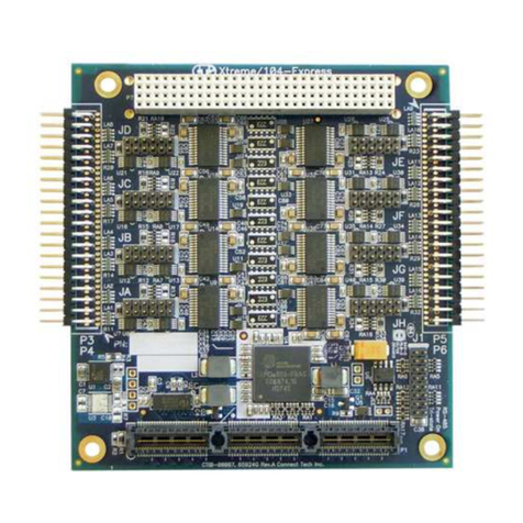
Mostek RAM-80BE User manual

@
Z8O IVI I CROCO MI PUTER SYSTE lVI S
Operations Manual
5
EXP\NSION
L

b
t
MEMORY EXPANST0N B0ARD (RAM-808E)
(I,iKiB110)
OPERATIONS IVIANUAL
t,
l',rK7B55c

I
L
L
SECTI ON
NUMBER
PARAGRAPH
NUMBER
t-t
t-3
t-4
t-5
l-6
2-1
2-3
2-5
2-6
2-7
2-8
2-9
2-11
2-12
2-13
2-14
?-15
3-l
3-3
?-E
3-6
3-7
10
J-O
3-9
3-t0
I
TABLE OF CONTENTS
TI TLE
GENERAL INFORMATION
I NTRODUCTI ON
GENERAL DESCRIPTION
FUNCT I ONAL
PHYSICAL
SPECIFICATIONS
FUNCTIONAL DESCRIPTION
I NTRODUCTI ON
MEMORY INTERFACE
MEIVIORY ARRAY
IVIEMORY DECODE AND CONTROL
ADDRESS MULTIPLEXER (MUX)
DATA BUFFER
PARALLEL I/O INTERFACE
plK3SUl P I0', s
PORT SELECT
BIDIRECTIONAL BUFFERS
STRAPP ED BUF FEP.S
DATA AND CONTROL BUFFERS
UTI LIZATION
INTRODUCTION
PARALLEL INTERFACE
CONNECTORS
RESISTOR TERMINATIONS
HANDSHAKE LINE BUFFERS (STB, RDY)
PORT A DATA BUFFER
PORT B DATA BUFFER
HEADER AND JUMPER INFORMATION
PAGE
NUMBER
1-1
1-1
I -t
I -t
1-1
2-1
2-1
2-1
z-1
2-1
2-1
2-3
o')
2-3
t-3
2-3
z-3
3-t
3-t
3-t
3-t
3-t
3-3
3-3
3-4
2
!

1t
SECTION
NUMBER
3 CONT'tl
APPENDIX A
APPENiJIX B
APPEI'iDIX C
PARAGRAPH
NUMBER
3-t I
3-12
3-t3
3-t5
3-t 6
3-17
a 1()
J-lo
3-t9
TABLE 0F C0NTENTS (C0NTD)
TITLE
PORT ADDRESSES
HEADER ANI] JUMPER iNFORMATI(-)N
MEMORY INTERFACE
MEMORY iJECijDING JUiviPERS
PAGE MODE
HTADER ANI] JUMPER INFORMATI(]N
MEIVIORY DISABLE iNPUTS
ADDIIIG MEiVlOiiY T() THI RAIVi-IJ(]B USING
THE XRAM-I]OB ADD ON P]EI,IORY PACKAGE
FACTORY NOTICES
SCHEMATIC DIAGRAMS
ASSEMBLY
\,
PAGE
NUMBER
2(r
J-U
3-13
3-13
3- 13
3-17
3-17
3-17
3-22
A-1
B-1
c-1
v
v

jjj
5LIST OF FIGURES
TITLE
RAM.SOBE CIRCUIT BOARD
RAM-8OBE FUNCTIONAL BLOCK DIAGRAM
GENERALIZED PARALLEL I/O INTERFACE
STRAPS TO CONTROL PARALLEL PORTS
PARALLEL I/O INTERFACE #I AS SHIPPED FROM THE FACTORY
PARALLEL I/O INTERFACE #2 AS SHIPPED FROM THE FACTORY
PARALLEL I/O INTERFACE
DECODED PORTS AVAILABLE FOR PIO #I, PIO #2, AND PAGE MODE
HEADER STRAPPING OPTIONS FOR PIO #I, PIO #2, AND PAGE MODE
PORT SELECT
HEADER STRAPPING OPTIONS FOR POSITIONING RAM-8OBE MEMORY
SDB-80E SYSTEM USING F0UR RAM-808E's IN PAGE M0DE
STRAPPING FOR ENABLING AND DISABLING PAGE MODE
HEADER STRAPPING OPTIONS FOR PAGE SELECT O-7
HEADER STRAPPING OPTIONS FOR PAGE SELECT 8.F
SDB-8OE CONFIGURED TO DISABLE OVERLAPPING RAM.SOBE MEMORY
F I GURE
NUMBER
I -l
2-1
3-t
,) ,)
J-J
3-4
5-O
3-7
3-8
3-9
3-t0
3-t I
3-12
3- 13
3 -14
PAGE
NUMBER
1-2
?-2
3-2
3-6
3-9
3-l 0
3-t I
3-12
3- 14
3- 15
L3-16
3-t8
3-t9
3-?O
3-21
3-?3
!

iv
TABLE
NUMBER
t-t
1-2
l-3
3-t
.) ,)
J-L
3-3
3-4
2r:
3-6
3-7
LIST OF TABLES
TITLE
AVAILABLE ITEMS
SPECIFICATIONS
CONNECTOR SKl & SKz PIN OUT
STRAPPING OF HANDSHAKE BUFFERS AS SHIPPED FROM FACTORY
DEVICE OPTIONS FOR PORT B
JUMPER OPTIONS FOR HANDSHAKE BUFFERS
JUMPER OPTIONS FOR PORT B CONTROL LINES
JUMPER OPTIONS F()R PORT A CONTROL LINES
DECODED PORTS AVAILABLE FOR PIO #I, PIO #2, AND PAGE MODE
EXPANDING RAIVI-8OBE MEMORY
\,
PAGE
NUMBER
t-3
t-3
l-4
3-3
3-4
3-5
3-7
1o
3- 13
3-24
v
t

L
t-t
SECTION 1
GENERAL INFORMATION
I.I . INTRODUCTiON.
1-2. The RAN'I-BCBE shown in Figure l-l provides a low cost nreans of expanding RAl4
and para11e1 I/0 for a ZB0 microcomputer systenr. The RAPl-80tsE is a peripheral
board wh'i ch can be d i rect'ly 'i nte rf aced to t he M0STEK ZB0 Sof tware Devel opme nt
Board (SDB-B0E) or any ZB0 Microprocessor based system.
I-3. GENERAL DESCRIPTION.
l-4. FUNCTI0i'lAL. The RAl,i-B0BE is a cornbj nat jon n:emory and I/0 expansion board.
The mernory niay be configured to have a rilemory capacity of l6K, 32K,48K, or 65K
bytes of RAivi. This on-board memory expandabil ity is rnade possible by population
options of ejther eight, sixteen, twenty-four or thirty-two i,lK4l l6-4 (16,384x1 i\10S
dynarnic RAI"I) menrories. The RAM-B0BE provides strapping options for positioning
the decoded memory space to start on any l6K address boundary. In addjtion to the
add-on memory, the RAM-B0BE provides four B-bit I/0 ports from the two on-board
l,iK3BBl ZB0 PI0 circuits. Each I/0 port 'is fu11y TTL buf fered and has two
handshake ljnes per I/0 port. The RAM-B0BE also includes logic for a "Page Mode
0peration" which permits up to l rnega-byte (sixteen 65KxB RAltl-B0B[s) to be used'in
a singie SDB-B0E system.
l-5. PHYSICAL. The RAM-B0BE is implenrented on a double Eurocard pri nted ci rcur't
board. The board requires three DC voltages at levels of +5, +12, and -12 VDC.
The RAIvI-B0BE'is interfaced to a system by connectors SKl and SK2.
I.6. SPECIFICATIONS.
1-7. Table l-l I ists nornenclature and part numbers for tlre RAM-B0BE and 'its
accessorjes. Table l-2 lists the overal 1 specif jcations for the RAivl-B0BE. Table
l-3 lists the pin usage of connectors SKl and SK2.
tt
L
t-2
Figure 1-1. RAM-B0BE Board. \r
v
v

I
t-3
\, Table 1-1. Available Items
Table 1-2. Specifications.
L
b
NAME
RAM.BOBE
**
DESCRIPTI ON
Expandable .l6,384 byte RAM board with 8-MK4116s,
sockets for 24 addjtional MK4ll6s, 2-MK38B1 ZB0
PI0s, p1 us page mode capabi 1 i ty.
PART NO
MK7B1 10
XRAM-BOB** RAM-B0Bt Expans ion Package, i ncl udes B-MK4l l6 RAMs MKTBI 26
for j nsert1on 'in the RAM-B0BE board pl us a blank
strappi ng header and document at'ion.
The XRAM-BOB package is available to RAM-B0BE customers only. It is therefore
required that each order for an XRAM-B0B be accornpanied by an /\uthorization
Cert'ifjcate from the RAM-B0BE package. (Each RAM-B0BE package is shipped with
three of these non-transferable, non-replaceable certificates. )
Mernory Capaci ty
I'lemory Acces s
Mernory Cyc 1e
Paral lel I/O
Interface levels
Physical Djrrensions
0perat i ng Ternperature
Up to 65,536 bytes
345 ns max.
450 ns min.
Four 8-bjt ports w/handshake lines
TTL compatible
+12 VDC +_5%,200 rnA (typ); 575 mA (max)
-12 VDC +_ 57,, 25 mA (typ); 30 mA (rnax)
+5 VDC +_5%, l.lA (typ);.|.5 A (max)
250 mnr x 233.4 rnr x 18 mm
0Cto50C

t-4
GND
GNt)
-t2Y
+5V
+5V
+t2v
I EOB
RESETI]
iVlR EQB
I I\TB
DB
I ORQB
WRB
R FSHB
DINB
Table 1-3. Connector SK1 and SK2 Pin Out. \
c
a
C
a
SK1
10
11
T2
13
74
1(
16
t7
1()
IU
19
20
2l
LL
)').
,) /t
L+
25
sK2
11
t2
13
t4
15
16
l1
1B
19
20
Z1
22
c')
LJ
24
25
1
2
a
J
1
2
a
J
4
5
4
5
6
7
B
GND
GND
-l2u
+5V
+5V
+l2Y
IEIB
MEIviD I 52
IliEMD I SB
t41B
RDB
AOB
AiB
A2B
A3B
A4B
A5B
A6B
ATrl
A8B
GND
GND
RD Y2B
P (D6 )4
P(D6)5
P (D6 )6
P(D6)7
RDY2A
P (D4 )4
GND
GND
\
BAI9
BAO
PD4) 5
D4 )6
D4)7
STB28
P (D6 )3
P (D6 )2
P(D6)1
P (D6 )o
STB2A
P (D2 3
P(D4)3
P(D4)2
P(D4)o
\
STBlB
PP(D4)1
P
RDYlB
P (D2 )4
P (D2 )5
D()B P (D?)2

LTable 1-3. Connector SK1 and SKZ Pin Out (Cont'd)
l-5
P(D2)1
P (D2 )o
STBlA
P (D0 )3
P(D0)2
P(D0)1
P(D0)0
SK2
c
ac
a
SK1
D1B
D2B
D3B
D4ts
D5B
D6B
D7B
26
27
28
29
30
31
22
A9B
/r108
A1 1B
A12B
Ai 3B
A1 4B
A1 58
P(D2)6
P (D2)7
RDYlA
P (Do )4
D0) s
D0 )6
D0)7
P(
P(
P(
26
27
28
29
30
31
1C
JL
L
L

') ')
L-L
Ir
Figure 2-1. FUNCTIONAL BLOCK DIAGRAM.
sl( 2
\
4
!
3
c0ilTR U ItS ADDRTSS
BUS OITA
8US
st( I
\
2
BI0tRtcTl0ttAL
EUTFER Bt0tntcIl0llAt
EUtttn STRA PPTD
BUTTER
STRA PPtD
BUTTTR
2
Mt( 38 I0
P81 M 1(3881 Pt0
2,)
P(}RT
stttcl
I
RY
Dtc
&
c0r{T
M tM ORY ARRAY
16|(xE E-ill(4ll6s
321{r8 16-ill(4116s
48l(x8 24-lll(4l16s
65l(x8 32-14111rrt,
RAS
CAS
WRITT D
c0t{IR0l.
55
3
C() TR(}t
illJx EUfrtR
EUfFtR BUfTTR BUTIER
4
5
8
8
22

L2.9. PARALLEL I/O INTERFACE.
2-10. The following functions from Figure ?-1 rnake up the
interface: MK3BBI PI0's, port select, bidirect'ional buffers,
data buffers and control buffers.
L-J
RAM-B0BE paral 1e1
strapped buffers,
L
?-11. tiK3BBl PI0's. The l,iK3BB1 para'l 1e1 input/output device is the central part
of the PI0 interface. The PI0 provides two B-bit ports with two handshake lines
per port.
2-12. PORT StLECT. The port select funct'ion is responsjble for selecting one of
the PI0's if the selected port address and the appropriate control signals are
present. The port sel ect i s al so used to sel ect one port for the page mode
ci rcuit, 'if the page rnode 'is bei rrg used.
Z-13, UIDIRTCTI0NAL BUFFERS. Tire bjd'irectjonal buffers are connected to port A
of the PI0's and can be used as either an input, output, oF bid'irectional
tri-state B-bit port. The bidirectional buffers are configured by the use of
juntpers contained on DIP headers. Strapping of the jurilpers is illustrated in tlie
utilization sect'ion.
2-14. STRAPPED IIUFFERS. Tlre strapped buffers are connected to port B of the
PiO's and can be used as ejther an input or an output port. Furthernrore, the port
Inay be divided into two four bit sections, wlth one section an input, and one
section an output. 0ptions for the strapped buffers are shown'in the utiljzation
section.
2-15. DATA ANU CONTROL BUFFERS. The data and control buffers,'isolate the data
bus and the control bus from the PIO's.
!

5
3-t
SECTION 3
UTILIZATION
3-I. INTRODUCTION.
3-2. Th js section wil I explain the various options for the memory and paral'le1
I/0 sections of the RAM-B0BE.
3.3. PARALLEL INTERFACE.
3-4. Two Paral lel I/0 Control lers (MK38B1 ) are jncluded on the RAt'/l-B0BE. This
gives four independent B-bit I/0 ports with two handshake (data transfer) control
I j nes per port. Al I I/0 I i nes are TTL buffered and have provis'ion for term'inat'ion
resistors on board. Figure 3-l shows a diagranr of a generalized para11e1 I/O
port.
3-5. C0NNECTOR. Connector SKz 'i s used for I/O and i s ident jf ied as Paral lel
I/rJ#] and Paral lel I/01f2.
3-6. RESIST0R TERI,lINATI0NS. 0ne 14-pin socket per port is provided for resistor
dual inl'ine packages so that terminations nay be placed on the data l'ines. A par-
allel termination is prov'ided for each B-b'it port data line plus the input strobe
(STB) handshake line. As sholn in Figure 3-1, the ternrination resistors may be
ejther s'irrrple pu11 up res'istors (port A) or an impedance matching network (port
B). The RAM-B0BE is shipped w'ith four 1KLpu11 up term j nat'ions. In add jtion to the
para11e1 termjnation res'istors each ready (RDY) handshake outpu+. ljne js
"terrninated" with a series 47Lresjstor on the board. This js used to help damp
and reduce any reflections on this output ljne.
3'7. HANDSHAKE LINE BUFFERS (SIB, RDY). Standard TTL txclusive 0R gates (7486)
are used to buffer and 'isol ate these I j nes. Juntper opt ions (l ocated on the J umper
Select Header) are provided on board to independently control the po'larity or
"sense" of each handshake signal so as to ease the interfacing between the board
and peripheral devices. The input Control and Data lines to each gate are ritarked
L
L

\
3-2
THE EXCLUSIVE ,OR' DEVICES CONTROL THE
POLARITY OR .SENSE'OF EACH HANOSHAKE LINE.
Figure 3-1. GENERALiZED PARALLEL I/0 INTERFACE.
+5 +5 f- - -r- - -
I
I
STF
I
I
I
c".L
/1E
/ ,o,
l_
\r
\1
I
I
RESISTOR
RM]NAT ON
RDY
IN OIP SOCKET
- - -t
I
HANDSHAKE
CONTROL
!TNDSHAKE
IK
I
I
I
I
bara
l0R
r
5!
IK
I
I
I
I
I
I
SK2 I
I
I
I
I
L]ATA
I aR
a!NIR,lL
I
I
I
I
I
I
I
I)
\
+5\
zzotl
I
I
33O^
.t
I
I
I
I
c
\
D
+
EA EB
ROY A STB
PORT A
POR 1 B
g srB e nov
JU M PER
BIDI
Pto
MK388
8u5
CO\ T R(lr
STB
,l
.l
8833
BUFFERS
Bt0r
BIDIRECTIONAL
JUMPER ]
/
.a/

5
1')
C and D respectively 'in Figure 3-1 controls the data as shown:
Control = Iogic "0"; Data = non-inverted
Control = logic rrlrr; Data = inverted
Table 3-.l. indicates how the handshake buffers are jumpered on the RAM-B0BE as
shipped frorn the factory.
Table 3-1. Strapping of Handshake Buffers as Shipped From Factory
DATA L I NE POLARITY OF BUFFER
PIO # IA RDY
A STB
B Rt]Y
B STB
i nvert i ng
'invert i ng
i nvert i ng
non-jnverting
PTO#2 A RDY
A STB
B RDY
B STB
non-jnverting
non-'i nvert i ng
non-inverting
non-jnverting
3-8. P0RT A DATA BUFFER. Port A data bus ljnes are buffered using two quad party
line non-inverting transceivers (DSBB33). Thjs al lows true bidjrectional
capabil'ity. Jurnper options allow for fixed IN, fixed 0UT or BIDIRECTI0NAL under
software contro'I. Replacing the DSBB33 with a DSBB35 effects a polarity change jn
the output bits. The drivers and receiver (as designated by D and R respectively)
in Figure 3-1 are enabled by jurnpers on the Jumper Select Header and on two sets
of tJire Wrap pins (E A-8, E C-D). The enable Iines are listed as REC for recejver
enable and DVR for driver enable. The jumper connections will be detailed later
under Header and Jumper I nforrnat'ion.
3-9. P0RT B DATA BUFFERS. Port B data l'ines are arranged in such a fashion (in
'increments of 4-b'it sections ) as to al lolv the user to determi ne the port
directjon. Sockets are provided for standard 14-pin 7400 series TTL packages.
Depending upon the package type jnserted, the port rnay be dedicated IN or 0UT.
L
L

3-4
In the output nrode ports may be selected to provide standard, or buffered drive,
active pu11 ups or open collector, low or high voltage, etc. Figure 3-1. shows an
arbitrary arrangernent whereby four bits are buffered OUT by a 7400 NAt'lD gate while
four bits are buffered IN by 7402 NOR gate. The Data Control lines of these gates
are marked D and C respectively. The control line for a NAND gate wi1'l be pu11ed
high by the pu11 up resistor, the control line for a NOR gate needs to be pu1'led
1oul, while the control l'ine for an Exclusive - or gate will determ'ine the output
polarity. Table 3-2. shows the djfferent types of dev'ices that may be used to
buffer port B.
Table 3-2. Device 0ptions for Port B.
IN OUT
3-'10. HEADER AND JUMPER INF0RMATI0N, Headers U17 (for I/0 #1) and U70 (for I/0
#2) contain the fol lowing jurnper opt'ions:
l) Determine polarity of handshake lines by strapp'ing the control line of
the Exclusive 0R buffers U20 and U69.
2) Strap the control ljne on the buffers of port B for proper AND, N0R, or
EX-0R operation.
3) Enable the Receiver or Driver portions of the port A buffers.
t
ts
Y
7402 STD drjve, inverting (NOR) STD dri ve, i nve rt i ng (l,lAND )
open collector, inverting (NAND)
STD drive, non-inverLing (AND)
open co1 lector, non-inverting (Al,lD)
7426 open co1 lector, high-vo1tage,
'inverting (NAND)
STD drive, non-inverting (0R)
buffer, inverting (NAND)
open coi lector, buffer, i nvert i ng
( NAND )
STD drive, Invert/non-inverLing
( Ex-0R )
7400
740 3
7408
7409
7 432
7437
7 438
7486

5
?tr
Figure 3-2. shows the header and l^jire l^jrap pins junrpered so that each control Iine
is strapped to logical r'0rr. Table 3-3,3-4 and 3-5 summarize al1 jumper options
for tlie t'rro I/0 interfaces. iiefer to Figure 3-3 and 3-4 which show the electrical
configuration of each interface as shipped frorn the factory for a RAM-B0BE.
Table 3-3. Jumper 0ptions for Handshake Buffers.
5
5
Des i gnator Header and Jumper P'ins
PIO #1
PTO #2
t
ARDY
I NVERTED
NON. I NVERTED
u77
Pi n 4,13 0PEN
Pin 4,13 STRAPPED
STB
I NVERTED
IiON. I NV E RT TD
u17
Pin 1,16 0PEN
Pi n 1,16 STRAPPED
D
DRDY
I NVERTED
NON- I NVERTED
ut7
P.in 3,14 0PEN
P'in 3,14 STRAPPED
BSTfs
I NVERTED
NOI'I-I NVERTED
u17
Pin 2,15 0PEN
P'in 2,15 STRAPPED
nRDY
I t\VERTED
NON- I NVERTID
u70
Pin 4,13 OPEN
Pin 4,13 STRAPPED
ASTB
I NVERTED
Nt)N.I NVERTED
u70
Pin 1,16 0PEN
P'in 1,16 STRAPPED
BRDY
I NVERTED
NON-INVERTED
STB
I NVERTED
NON- I NV E RT ED
B
u70
Pin 3,14 0PEN
Pin 3,14 STRAPPED
u70
Pin 2,15 0PEN
Pin 2,15 STRAPPTD

3-6
Figure 3-2. STRAPS T0 C0NTR0L PARALLEL PORTS.
HEAOER UI7 OR U7O
9A RDY BsrB t
B RDY A STB
CONTROL LINE FI)R EACH HANDSHAKE BUFFER IS STRAPPED ]O A LOGIC,,O'. SO
HANDSHAKE DATA IS NON-INVERTED. ABSENCE OF A STRAP INVERTS THE DATA.
4
HEADER UI7 OR U7O
a
4
I
A.
B.
a
D.
tz
R
I
l2
u27 0R U29
u22 0R U24
CONTROL LINE FOR EACH HANDSHAKE BUFFER IS STRAPPED TO A LOGIC..O..SO
THAT THE 'oR' oR 'NoR' BUFFER ls ENABLED. ADDITtoN oF A srRAp
APPLIES To A'AND,,'NOR. oR PoSSIBLY AN EX .OR. GATE.
9
84
HEAOER UI7 OR U7O
tz r6
V REc
DVR
BorH THE RECEtvER AND DRtvER coNTRoL LTNES ARE srRAppED To "o" cAUStNG
THE RECEIVERS AND DRIVERS TO BE ENABLED, IN OPERATION EITHER ONE MAY
BE STRAPPEI) BUTI'IOT BOTH. IN THE tsIDIRECTIOIIAL MODE NO STRAP IS USED.
EI E3 Eg E7
E4 E6 ,
I
::::IIII
::II::::
II::::::
WIRE WRAP PINS ARE WIRED FOR BIDIRECTIONAL MODE
r6
E8

3-7
5Table 3-4. Jumper 0ptions for Port B Control Ljnes.
b
L
BUFFER AND SOCKET HEADER AND JUMPERS
7400, 7403,7408,7409
7426, 7437 , 7438
U?7
u22
u29
u24
U17 Pin 5,12 OPEN
U17 Pin 6,11 0PEN
U70 Pi n 5,12 0PEN
U70 Pin 6,11 0PEN
7402, 7432
u27
u22
u29
u24
U17 Pin 5,12 STRAPPED
U17 Pin 6,11 STRAPPED
U70 Pin 5,12 STRAPPED
U70 Pin 6,11 STRAPPED
7 486 u?7 (TNVERTiNG)
u27 (N0N-TNVERTTNG)
u22 (TNVERTTNG)
u2? (N0N-TNVERTTNG)
u7e (TNVERTTNG)
u?9 (N0N-TNVERTTNG)
u24 (TNVERTTNG)
u?4 (N0N-TNVERTTNG)
u17
u17
ut7
u17
u70
u70
u70
u70
Pin
P'i n
Pr'n
Pin
Pr'n
Pin
Pin
Pin
5 rl?
5,12
6,11
6 ,11
5,r2
5,12
6,11
6 ,11
OP EN
STRAP P ED
OP EN
STRAP P ED
OP EN
STRAP P ED
OP EN
STRAP P ED
Table of contents
Other Mostek Computer Hardware manuals