SP16160CH1RB Reference Design Board User’s Guide
- 6 -
www.national.com
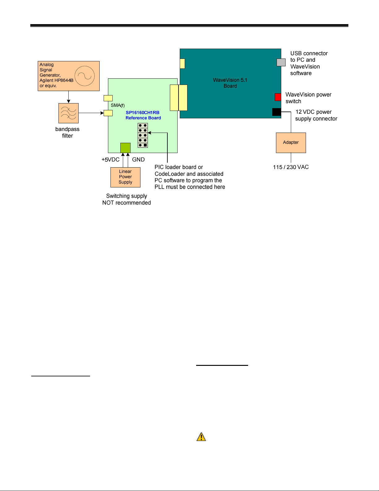
• Connect the WaveVision 5.1 Digital Interface
Board to your PC through the supplied USB cable
and apply power to the WaveVision 5.1 board
through the +12V AC-DC power adapter included
in the WaveVision 5.1 hardware kit. The
connection diagram is shown in Figure .
If this is the first time connecting a WaveVision 5.1
board to your PC, follow the on-screen instructions for
installing the drivers for the hardware.
For more information on installing the WaveVision data
acquisition hardware or software, please refer to the
Quick Start Guide in the WaveVision User’s Guide
which can be found on the National Semiconductor
website at http://www.national.com/
appinfo/adc/evalboards_datacapture.html.
Please note that the SP16160CH1RB is only
compatible with National Semiconductor’s WaveVision
5.1 Digital Interface board.
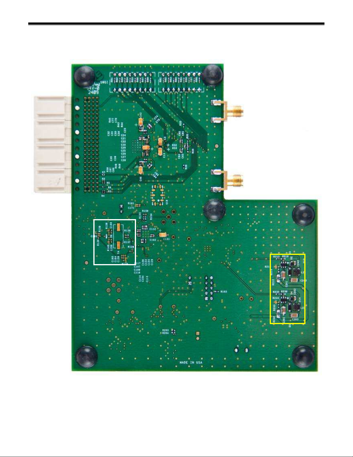
5.2 Reference Board Jumper Positions
• Verify that the JP1 jumper is installed to provide
power to the PIC microcontroller board. The PIC is
used for programming the LMK0 031B registers.
Remove JP1 if using CodeLoader to program the
LMK0 031B (see Section 8.2 of this guide).
5.3 Connecting Power and Signal Sources
• Connect the SP16160CH1RB reference board to
the WaveVision 5.1 board through the FutureBus
connector as shown in Figure . The
SP16160CH1RB reference board should not be
powered up, as the WaveVision hardware does not
support hot-swapping of boards.
• Power up the WaveVision 5.1 board and connect it
to the PC with a USB cable.
• Plug the PIC microcontroller board onto the dual-
row header labeled “H3” as shown in Figure 5.
Align the arrows on the two boards to ensure
proper orientation. JP1 should have a jumper
installed on the main board to provide power to the
PIC microcontroller board. Lastly, flip the switches
on the PIC microcontroller board to the following
positions: Switch 1 = ON, Switch 2 = ON.
• Connect a 5.0V power supply capable of sourcing
up to 1A to the green, 2-terminal power connector
located along the side edge of the SP16160CH1RB
board. This is shown in Figure . Ensure that the
polarity of the wires going to the green power
connector match the “+5V” and “GND” labels on
the reference board. After the polarity is verified,
turn on the 5V supply.
• Press the “RESET” button on the PIC
microcontroller to load the register settings into the
LMK0 031B. The three LED’s on the PIC
microcontroller board will flash four times to
indicate that the register bits have been sent to the
LMK0 031B. If the lights to not flash, ensure that
JP1 is connected to supply power to the PIC board.
• Connect the signal source to the “SMA_AMP_I”
SMA connector indicated in Figure 1. The
recommended signal generators are the HP86 B
(HP/Agilent) or the SMA100A (Rohde & Schwarz).
A bandpass filter between the signal generator
output and the SP16160CH1RB SMA connector is
required to measure the true performance of the
board. A Trilithic bandpass filter is recommended.
See Figure .
• Set the signal source frequency to 190 MHz and
the starting input amplitude to -15 dBm.
• Start the WaveVision software. The WaveVision
software will automatically load the appropriate
firmware to initialize data capture from the
SP16160CH1RB. Allow the firmware file to finish
downloading before continuing. When finished, the
board should be ready to capture digital data.
• Capture the data and display the FFT of the
captured data with the WaveVision software.
Align Pin
Place JP1 on
main board to
provide power
Switch 1 = ON
Figure 5: PIC microcontroller Board Connection
and Configuration