New Micros NMIN-0812 User manual

NMIN-0812
Single Board Computer
NEW MICROS, INC. 1601 Chalk Hill Road. Dallas, TX. 75212
Tel: (214)339-2204 Fax: (214)339-1585 www.newmicros.com

2
TABLE OF CONTENTS
CONTENTS PAGE
Introduction 3
Getting Started 4
Serial boot loader 5
Interrupts Vector Table 6
Memory Map 7
Serial I/O 8
Power supply 9
BDM Connector 10
I/O Connectors 11
Silk Screen 12
Schematic 13

3
INTRODUCTION
The NMIN-0812 board is a MC68HC812A4 16-bit based single board computer with built-in 4-Kbyte EEPROM, 1-
Kbyte RAM, two Asynchronous Serial Communications Interfaces (SCI0 and SCI1), a Serial Peripheral Interface
(SPI), a Single-Wire Background Debug Mode, 8-channel 8-bit A/D Converter.
Features
16-Bit CPU, Single Chip Mode.
Memory
o 32-Kbyte flash EEPROM with 2-Kbyte Erase-Protected Boot Block loaded with Serial Boot Loader.
o 768-Byte EEPROM
o 1-Kbyte RAM
8-Channel 8-Bit Analog-to-Digital Converter.
8-Channel Timer
o Each channel Fully Configurable as either Input Capture or Output Compare
o Simple PWM Mode
o Modulo Reset of Timer Counter
16-Bit Pulse Accumulator
o External Event Counting
o Gate Time Accumulation
Pulse-Width Modulator
o 8-Bit, 4-Channel or 16-Bit, 2-Channel
o Separate control for each pulse width and duty cycle.
o Programmable center-aligned or left-aligned outputs
Serial Interfaces
o Two Asynchronous Serial Communications Interface (SCI)
o Synchronous Serial Peripheral Interface (SPI)
COP Watchdog Timer
Single-Wire Background Debug Mode (BDM)
On chip hardware breakpoints

4
GETTING STARTED
To begin, communications must be established through a terminal , or PC using a communications package. The PC
gives a better environment for a serious development. A terminal is all that is necessary for board evaluation. In the
latter case, begin by connecting the terminal via the serial RS-232 DB9F connector on the NMIN-0812. Most
terminal should plug in directly via a straight through cable (i.e.: pin 1 to 1, 2 to 2, 3 to 3, etc…). Most terminals
have a female connector, as does the NMIN-0812, so the cable will need male connector at one end and female at
other end. Alternately, a gender changer might be used to serve the same purpose.
A PC running a communications program can be used instead of a terminal. The new standard PC’s serial jack is a
DB9M male connector and It should plug in directly to the NMIN-0812 via a straight through cable with a female
on one end and the male at the other end.
To power the NMIN-0812, you need a 9 to 12V transformer plugs into the power jack, PJ1 or a regulated +5VDC
applies to J2, pin 1 & 2 for GND & 5V, respectively.
The terminal must have the correct communications settings. The baud rate should be set at 9600 baud. The NMIN-
0812 sends and receives a bit protocol of one start bit, eight data bits, and one stop bit.
START STOP
Bit Stream
When the terminal is set correctly, and power is applied the NMIN-0812 should response with:
(E)rase or (P)rogram (R)eset:
When you depress the ENTER key, it should also response with
(E)rase or (P)rogram (R)eset:
Seeing that message means the communication is established.
3
2
4
8
5
1
67

5
SERIAL BOOTLOADER
The Serial Boot loader occupies 1K-bytes of erase-protected EEPROM starting at address $FC00. Thus, user code
may only occupy the 3K-byte from $F000 to $FBFF.
The Boot loader contains a serial S-Record loader that can load assembled code from the host computer into
EEPROM. It uses the SCI for communications with the host computer via the NMIN-0812 RS-232 interface. The
only special requirements for the host computer’s communications program are:
It must operate at 9600 baud
It must wait for the prompt string, the ASCII * character before sending a line of text to the NMIN-0812. This
“handshaking” is necessary because of the variable amount of time required to program each S-Record into
Flash EEPROM. Flash EEPROM typically requires 10ms per byte.
If you use the terminal program called MAXTERM, or NMITerm, you must change the PACING character to
decimal 0. Line Delay set for 100ms.
(E)rase, (P)rogram ( R)eset:
Select the desired function by typing an upper or lower-case “E” or “P”.
Note: The starting address of the user code must be placed in the reset vector position ($FBFE) of the alternate
reset/interrupt vector jump table. For more information, see Vector Jump Table: Interrupt and Reset Address
on page 7.
The boot loader cannot be used with S-Records containing a code/data field longer than 64 bytes. Longer S-
Record will cause the boot loader to crash and/or program incorrect data into EEPROM.
S-Record may contain ASCII “CR” and/or “LF” characters.
(E)rase: This selection causes a bulk erase of EEPROM except for the erase-protected area starting at address
$F800, which contains the boot loader program, and the reset/interrupt vector table. After the erase operation, a
verify operation checks for proper erasure of all locations.
If the erase operation was successful, the message “Erased” is displayed, and the boot loader’s prompt is
redisplayed.
(P)rogram: In flash programming mode, the boot loader sends an ASCII “0” (NULL character) to the host
computer, indicating that it is ready to receive an S-Record. The host then sends a single S-Record and wait for the
“0” prompt from the boot loader before sending the next R-Record.
This process is repeated until the boot loader receives and end-of-file (S9) record from the host computer. If no S9
record is received, the boot loader continues to wait for another S-Record indefinitely. In this situation, the NMIN-
0812 must be reset to return to the boot loader’s prompt. (S-Record already loaded into EEPROM are unaffected by
missing S9 record; reprogramming is not necessary).
Serial Boot Loader Recovery: To erase the application program, tie port PH0 to ground will always force the serial
boot loader to come up on reset. At the prompt enter (E)rase, then (P)rogram to reload the new program.

6
VECTOR JUMP TABLE: INTERRUPT AND RESET ADDRESSES
The CPU’s interrupt and reset vectors are located in the EEPROM and thus cannot be reprogrammed with the S-
Record boot loader.
To allow the user code to specify interrupt and reset addresses, each member of the vector table starting at address
$FF80 contains a pointer to a vector jump table, which is located in the user-programmable EEPROM starting at
address $FB80.
Each entry in the vector jump table occupies two bytes of memory, which is adequate for the addresses of the user
reset and interrupt service routines. The interrupt vector mapping is shown in the table below.
Vector Address CPU Interrupt Jump Table Address
$FF80 - $FFCD Reserved $FB80 - $FBCD
$FFCE - $FFCF Key wakeup H (stop wakeup) $FBCE - $FBCF
$FFD0 -$FFD1 Key wakeup J (stop wakeup) $FBD0 - $FBD1
$FFD2 - $FFD3 ATD $FBD2 - $FBD3
$FFD4 - $FFD5 SCI1 $FBD4 - $FBD5
$FFD6 - $FFD7 SCI0 $FBD6 - $FBD7
$FFD8 - $FFD9 SPI $FBD8 - $FBD9
$FFDA - $FFDB Pulse Acc. Input Edge $FBDA - $FBDB
$FFDC - $FFDD Pulse Acc. Overflow $FBDC - $FBDD
$FFDE - $FFDF Timer Overflow $FBDE - $FBDF
$FFE0 - $FFE1 Timer Channel 7 $FBE0 - $FBE1
$FFE2 - $FFE3 Timer Channel 6 $FBE2 - $FBE3
$FFE4 - $FFE5 Timer Channel 5 $FBE4 – $FBE5
$FFE6 - $FFE7 Timer Channel 4 $FBE6 - $FBE7
$FFE8 - $FFE9 Timer Channel 3 $FBE8 - $FBE9
$FFEA - $FFEB Timer Channel 2 $FBEA - $FBEB
$FFEC - $FFED Timer Channel 1 $FBEC - $FBED
$FFEE - $FFEF Timer Channel 0 $FBEE - $FBEF
$FFF0 - $FFF1 Real Time Interrupt $FBF0 - $FBF1
$FFF2 - $FFF3 IRQ $FBF2 - $FBF3
$FFF4 - $FFF5 XIRQ $FBF4 - $FBF5
$FFF6 - $FFF7 SWI $FBF6 - $FBF7
$FFF8 - $FFF9 Unimplemented Instruction Trap $FBF8 - $FBF9
$FFFA - $FFFB COP Failure Reset $FBFA - $FBFB
$FFFC - $FFFD Clock Mon. Fail Reset $FBFC - $FBFD
$FFFE - $FFFF Reset $FBFE - $FBFF
7
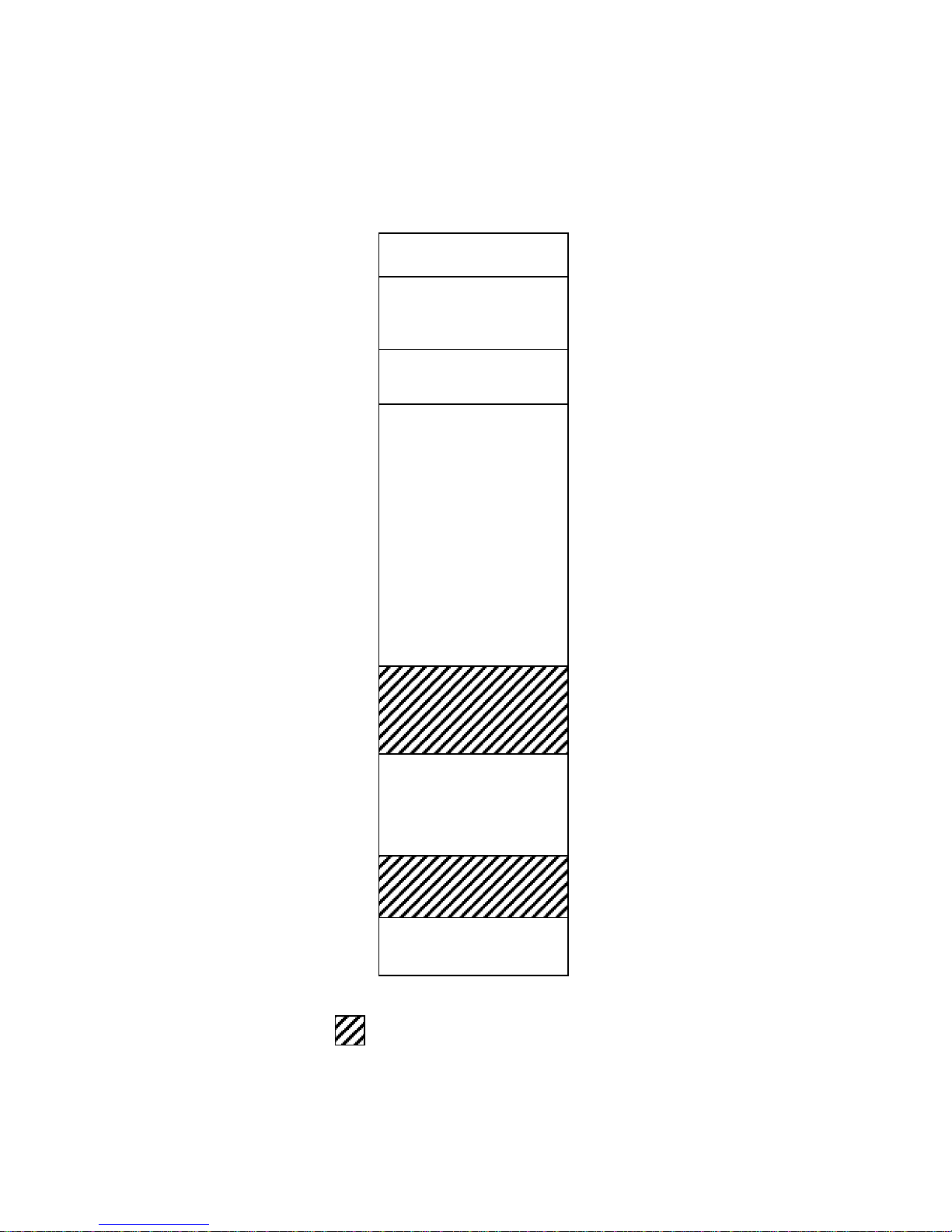
MEMORY MAP
$FFFF
$FF80
$FC00
$FB80
$F000
$0D00
$0800
$0200
$0000
Not Available
Main vectors
Serial Boot Loader
2
nd
Interrupt Vectors
Empty EEPROM
RAM
I/O REGISTERS

8
SERIAL I/O
The MC68HC812A4 has two full duplex hardware serial channels, and both are converted for RS-232 interface.
The RS-232 signals are brought out to DB1 connector, a standard serial DB9 connector , and J7 connector, a 2x5
header pin that can be used with the ribbon cable type. The primary serial SCI0 is assigned to DB1, where the SCI1
is assigned on J7.
DB1, SCI0 serial RS-232 signals
51
96
DB9F
DB9F Signal Name
-------- -----------------
Pin 1 No connection
2 SO0, Serial Output from NMIN-0812, TxD0 converter
3 SI0, Serial Input to NMIN-0812, RxD0 converter
4 to 6 DSR to DTR (loop back wire)
5 Electrical Ground
7 to 8 CTS to RTS (loop back wire)
J7, SCI1 serial RS-232 signals
To pin 4 To pin 6 To pin 4 NC NC
2 4 6 8 10
1 3 5 7 9
NC SO1 SI1 To pin 2 GND
2x5 header pin Signal Name
------------------- -----------------
Pin 1, 8, 10 No connection
2 SO1, Serial output from NMIN-0812, TxD1 converter
3 SI1, Serial input to NMIN-0812, RxD1 converter
4 to 6 DSR to DTR (loop back wire)
5 Electrical Ground
7 to 8 CTS to RTS (loop back wire)

9
POWER SUPPLY
The power supply circuit on the NMIN-0812 is designed to allow the board to operate from a simple, low-voltage,
AC/DC wall transformer.
Power jack, PJ1 is voltage input or for AC or DC voltage greater then 8 volts to be input.
The Bridge rectifier, DB101 converts AC to DC and the 78L05 regulates this rectified incoming voltage to a
constant 5 volts. The typical current required by the NMIN-0812 is 60mA.
For application that requires higher current than 100mA, the 78L05 TO-92 package needs to be replaced with
78T05 TO-220 package to handle this.
The upper limit of +V is set by the ability of the 7805 to dissipate heat. If a heat sink is added to the 7805, voltage in
excess of 20 Volts are possible. Driving the 7805 to hard, however, will cause it to enter thermal overload and “shut
down” its output.
Regulated 5VDC input is optional used instead of AC/DC transformer input. On board the connector J2, pin 1 & 2
are GND & 5V, respectively. This 5V pin is connecting to the entire 5V circuitry on board. Therefore you can
apply 5V regulated and GND to the power pin connections on J2.

10
BDM CONNECTOR, J4
J4 is Background
Debug Mode connector that can be interfaced with Motorola’s SDIL cable or P&E’s BDM cable.
J4
BKGD GND
NC RESET
NC +5V
11
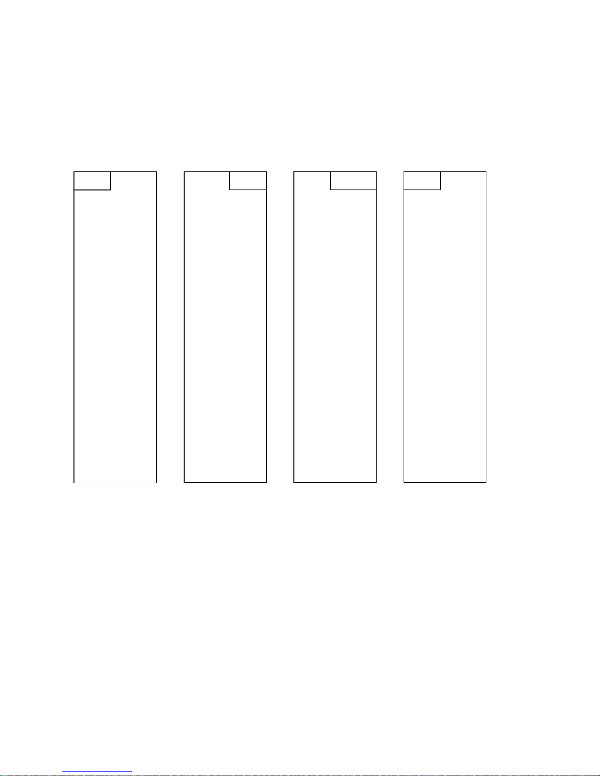
I/O PINOUT CONNECTORS: J1, J2, J3, J5
All the CPU I/O ports are brought out to J1, J2, J3, and J5 connectors.
J1 J2 J3 J5
PC0
PC1
PC2
PC3
PC4
PC5
PC6
PC7
PE0 PE1
PE2 PE3
GND +5V
PLL XFC
GND
ECK
MODA MODB
PE7 PB0
PB1 PB2
PB3 PB4
PB5
PB6
+5V
GND
PH7 PH6
PH5 PH4
PH3 PH2
PH1 PH0
GND PF6
PF5 PF4
PF3 PF2
PF1 PF0
PA7 PA6
PA5 PA4
PA3 PA2
PA1 PA0
PB7
GND
VSS
VDDX
PJ0 PJ1
PJ2 PJ3
PJ4 PJ5
PJ6 PJ0
PG0
PG1
PG2
+5V
GND
PG3
PG4
PG5
BKGD
PD0
PD1
PD2
PD3
PD4
PD5
PD6
PD7
GND
VRH
VRL
PAD0 PAD1
PAD2 PAD3
PAD4 PAD5
PAD6 PAD7
VDDA GND
RXD0 TXD0
RXD1 TXD1
PS4 PS5
PS6 PS7
PT0 PT1
PT2 PT3
PT4 PT5
PT6
PT7
Table of contents
Other New Micros Motherboard manuals

Popular Motherboard manuals by other brands

Freescale Semiconductor
Freescale Semiconductor i.MX 6UltraLite Hardware user's guide

ASROCK
ASROCK G31M-VS2 - V1.1 user manual

Linear Technology
Linear Technology DC1386B manual

ASROCK
ASROCK X79 Extreme4-M user manual

abaco systems
abaco systems SP9 Series Hardware reference manual

Sapphire Audio
Sapphire Audio Pure Black X79N user manual


