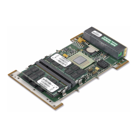
New Micros NMIY-0031 User manual

2/26/20022:06 PM 1
NMIY-0031
Single Board
Computer
Covers: NMIY-0031 V1.0 4/22/96

2/26/20022:06 PM 2

2/26/20022:06 PM 3
NMIY-0031 TABLE OF CONTENTS
Table of Contents
TABLE OF CONTENTS ..............................................................................................................................3
PART I ...........................................................................................................................................................5
INTRODUCTION .........................................................................................................................................5
CONVENTIONS...............................................................................................................................................7
GETTING STARTED ........................................................................................................................................9
BASIC USERS.........................................................................................................................................10
MONITOR USERS ..................................................................................................................................10
FORTH USERS.......................................................................................................................................11
PART II ........................................................................................................................................................13
HARDWARE...............................................................................................................................................13
CIRCUIT DESCRIPTION ................................................................................................................................15
POWER...................................................................................................................................................16
PROCESSOR ..........................................................................................................................................16
BOARD CONFIGURATION...................................................................................................................16
MEMORY SOCKETS ..............................................................................................................................17
I/O INTERFACES ...................................................................................................................................17
PROTOTYPING AREA ...........................................................................................................................18
I/ O CONNECTORS.......................................................................................................................................19
POWER - J12..........................................................................................................................................19
KEYPAD - J3 ..........................................................................................................................................19
LCD - J6..................................................................................................................................................20
RS232 - J10.............................................................................................................................................20
OPTIONAL CONNECTORS ...................................................................................................................21
RS422/485 - J11......................................................................................................................................21
VERTICAL STACKING CONNECTORS - J1, J7, J9..............................................................................21
LATCHED and NON-LATCHED I/O - J4 and J5 ..................................................................................22
JUMPERS .....................................................................................................................................................23
MEMORY CONFIGURATION JUMPERS .............................................................................................23
RESET.....................................................................................................................................................24
LCD CONTRAST ....................................................................................................................................25
VERTICAL STACKING COMPONENT (VSC) CONFIGURATION JUMPERS....................................25
SERIAL COMMUNICATIONS CONFIGURATION JUMPERS.............................................................26
TROUBLESHOOTING ....................................................................................................................................27
MOUNTING............................................................................................................................................27
POWER SUPPLY....................................................................................................................................27
OPERATING SYSTEM............................................................................................................................27
MEMORY................................................................................................................................................28
TERMINAL .............................................................................................................................................28
KEYPAD and LCD I/O ...........................................................................................................................28
PHYSICAL INSTALLATION OF DEVICES ...........................................................................................28
BOARD MOUNTING .....................................................................................................................................29
NMIY-0031 MOUNTING........................................................................................................................29
VSC MOUNTING....................................................................................................................................29

2/26/20022:06 PM 4
PART III ......................................................................................................................................................31
SOFTWARE ................................................................................................................................................31
PROGRAMMING ...........................................................................................................................................33
MEMORY................................................................................................................................................33
DATA PORTS..........................................................................................................................................35
KEYPAD I/F............................................................................................................................................35
LCD I/F...................................................................................................................................................36
SERIAL I/O .............................................................................................................................................38
PROGRAM SEGMENTS..................................................................................................................................39
MONITOR...............................................................................................................................................39
BASIC......................................................................................................................................................41
C..............................................................................................................................................................43
FORTH....................................................................................................................................................46
PART IV.......................................................................................................................................................49
DRAWINGS ................................................................................................................................................49
PARTS LIST .................................................................................................................................................51
SILK SCREEN...............................................................................................................................................53
MECHANICAL DRAWING .............................................................................................................................55
SCHEMATIC .................................................................................................................................................57
....................................................................................................................................................................57
APPENDICES .............................................................................................................................................59
APPENDIX A ..............................................................................................................................................61
APPENDIX B.............................................................................................................................................101
APPENDIX C ............................................................................................................................................147

2/26/20022:06 PM 5
NMIY-0031 PART I INTRODUCTION
PART I
Introduction
The NMIY-0031 board is a low cost, production oriented, computer board. Facilities are
included for serial communications, LCD interface, keypad, memory expansion to 64Kbytes of
data and memory each, and raw and latched parallel I/O. It can serve as host for the NMIL
series of Vertical Stacking Component (VSC) cards. This ability gives it a great degree of
flexibility in meeting customer application requirements. The NMIY-0031 design allows
purchasers to configure the board, including only the hardware facilities required by their
application.
The NMIY-0031 has several options that make it adaptable to many uses. The standard
configuration is used as a base to allow the user many paths to achieving the control configuration
that suits their application. To provide the facilities that promote application development, the
installed headers option allow flexibility in configuring memory. Three languages for
development, as well as a monitor, are also available. Other options include an on board power
supply, up to a 64K program EPROM, up to two 32K data ram chips, and three COM port
standards. Customized circuitry can be added in the prototyping area.
Vertical Stacking Component (VSC) options further enhance flexibility. More than a dozen
NMIL series peripheral cards are available to enhance off the shelf hardware solutions for control
systems. Custom card designs can also make use of the VSC connector for connection.
With the combination of 64K program space, 64K data space, and fully customizable interfaces,
the NMIY-0031 processor board provides the user with the ability to construct a cost-effective,
digital control unit for a wide range of applications.
Conventions describes the use of print conventions in this manual.
Getting Started provides some basic functional checks so that the user may quickly determine
the status of the hardware.

2/26/20022:06 PM 6

2/26/20022:06 PM 7
NMIY-0031 CONVENTIONS
Conventions
Several different type faces are used in this manual to distinguish items such as user input, screen
output, etc. This is a guide to reading the type-face conventions employed.
Conventions typeface is used to distinguish chapter titles at the beginning of each
section.
FORTH indicates the formal name of a language, or a title reference to another manual chapter or
chapter subsection title.
Enter highlighting signifies a key name for function keys. In a program dialog, highlighting
indicates a user keyed data entry.
OK indicates a response from software or operating system.
Bold text is used occasionally, where text requires special emphasis.
Command codes and addresses are always given in hexadecimal format.

2/26/20022:06 PM 8

2/26/20022:06 PM 9
NMIY-0031 GETTING STARTED
Getting Started
System operation requires power and communications connections. A standard configuration
board requires 250 mA of regulated +5 VDC at connector J12. The on-board power supply
option requires 6.3 to 10.0 VAC input at connector J2. The MAX232 chip develops its own +/-
10 VDC for RS-232C compatibility.
For development systems, a terminal (or PC with terminal emulation software) must be
connected. A cable with an RS-232 connector (DB25 or DB9) on one end and a 10-pin dual-row
header connector on the other end is required. This cable is not included with the NMIY-0031,
and must be provided by the user or purchased separately from the supplier. The RS-232 serial
connections are present at J10. Pin J10-3 is data-out and pin J10-5 is data-in to the 0031 board.
See the section on I/O Connectors for additional detail on J10 connections.
Once power and terminal connections are established, the operating system or monitor EPROM
in U2 can be used to work with basic board functions, such as the LCD or keypad interfaces.
The RS232 terminal connection requires a 9600 baud terminal with no parity, 8 data bits, and one
stop bit (8N1). On a PC, also check that the terminal emulator program is set to use the same
physical port to which you have attached the serial interface cable( i.e. COM1:, COM2:, etc.).
Examples follow for users of BASIC, Monitor, and FORTH. The examples are intended as quick
checks of board function. When the cursor (underscore) is present in an example, it will blink.
FORTH does not use a cursor.

2/26/20022:06 PM 10
NMIY-0031 GETTING STARTED
BASIC USERS
The BASIC EPROM should be installed in U2. BASIC also requires a 32K RAM chip be
installed in U4. EEPROM may be used in U3 at the user’s option. At power on, the terminal
(or emulator) will display:
*MCS-51 ™ BASIC V1.1* ÅBoard power on message at the terminal
READY
>_ ÅPrompt (‘>’) followed by cursor ( ‘_’)
To verify operation, enter the command:
>PRINT “HELLO!” ÅUser input
HELLO! ÅBASIC response; Note: no prompt on this line
>_
If you see something significantly different, please consult the section on Troubleshooting. For
additional information on BASIC please consult the MCS BASIC manual.
MONITOR USERS
For users with the Monitor EPROM in U2, power-on causes the system to start up and display
the message:
NMI 8051 MONITOR V1.10
TYPE ‘H’ FOR HELP
>_
Please note that the monitor commands must be upper case. We strongly recommend that the
user put the keyboard in CAPS LOCK mode when using the monitor. When the user enters H (no
enter needed), the following help menu appears on the terminal:
H
-------------------------------------------------------------------------------------------------------------
H :help
R <addr> :read internal data memory
D <addr> :read external data memory
P <addr> :read program memory
S <addr> :read special function register
A <addr> <size> :dump internal data memory
U <addr> <size> :dump external data memory
M <addr> <size> :dump program memory
W <addr> <size> :write onto internal data memory
O <addr> <size> :write onto external data memory
T <addr> <size> :write onto special function register
F <addr> <size> <value> :fill external data memory with value
X <addr> :execute
Z <addr> <size> :erase internal data memory
E <addr> <size> :erase external data memory
L :load INTEL HEX file
I <addr> <size> :dump memory in INTEL HEX format
-------------------------------------------------------------------------------------------------------------
>_

2/26/20022:06 PM 11
NMIY-0031 GETTING STARTED
Under monitor control, the computer’s response appears on the terminal screen as soon as the
complete command is entered. When using this monitor, an enter on the terminal keyboard is
NOT required to begin command execution. Execution begins as soon as all command characters
are fully entered at the keyboard. An enter before giving a valid command with its required data,
the monitor will issue an appropriate error message followed by a prompt. Whenever the
Monitor displays the prompt, it is ready for the next user command. The Monitor does not
recognize the backspace key.
Data format and position are crucial to success when using a monitor. Fields in angle brackets are
required and expect an exact number of characters. Numeric values such as addr, size, and value
are entered in hexadecimal (‘hex’). Example: <addr> expects a four digit hex value, <size>
expects a two digit hex value. Note that the hex digits greater than 9 require upper case. It is
recommended that the terminal be set to CAPS LOCK whenever hex values are to be entered.
FORTH USERS
At power on, EPROM based FORTH users will see:
Max-FORTH V1.0
This message should appear any time the card is reset including power on. The card should be
connected through J10 to a terminal or emulator at 9600 baud, 8-N-1. With the prototype area of
the board to your left, looking at the component side of the card, J10 is in the upper right hand
corner of the board. Also, J10-Pin1 will be toward the right edge of the card, away from the
processor, U1, and the prototype area.
A quick check that FORTH is operating is to enter the command WORDS. Note that this entry
will be in all caps. The screen will display a list of words (commands) and addresses provided by
the system. Expect the list to scroll off the screen:
WORDS
1E4E TASK 134F ( 1EAE Z 1EE2 IC!
1EE4 IC@ 589 @ 57C C@ 561 !
572 C! 151 2@ 140 2! F4E :
F64 ; 550 + 53E - 1B2F 1-!
1B25 1+! 1A9 +! 1E46 * 1E3C /
49E >< 4A8 SWA_ 1ACD 2OV__ 1AD9 2SW__
4FF DUP 1AC5 2DU_ 490 OVE_ 476 ROT
1AB7 2RO_ 196 PIC_ 16F ROL_ 1AF3 -R__
4E5 DRO_ 136 2DR__ 4CB >R 4D8 R>
1B39 = 390 NOT 385 0= 1EA6 D0=
375 0> 36A 0< 358 U< 332 <
DF DU< AA D< 1E9E D= 1B49 >
52D AND 50B OR 51C XOR 161C IF
1610 THE_ 15FA ELS_ 15F0 BEG__ 15E2 UNT__
15D0 REP___ 15C8 WHI__ 15BA AGA__ 15E2 END
1552 DO 1576 LOO_ 1566 +LO__ 229 K
220 J 1F9 I 1E5 R@ 1586 LEA__
630 EXI_ 790 KEY 789 EMI_ 770 ?T________
1B41 S->_ 322 ABS 1E8A DAB_ 318 MIN
1E78 DMI_ 308 MAX 1E66 DMAX 1D4A SPA___
1AE5 DEP__ 1CC5 CR 1CA5 TYP_ 1C99 COU__
1C71 -TR_______ 3BC 1+ 3D8 2+ 3C9 1-

2/26/20022:06 PM 12
NMIY-0031 GETTING STARTED
3E1 2- 3AB 2/ 39D 2* 103 D+
1AA5 D- 59B D2/ 1DF8 /MO_ 1DF0 MOD
1DE4 */M__ 1DDA */ 2BA UM* 27F UM/___
23A NEG_ __ 122 DNEG __ F8C CON______ F7C VAR______
F9A 2C________ F72 2V________ 232 EXE____ 4C3 RP@
4BA SP@ 1D9A CMO ___ 6F0 CMO__ 630 ;S
FC4 COD_ FB4 END-C___ FA6 USE_ 1B7B .
1B8D .R 1B99 D. 1B73 U. 1B83 U.R
1BA3 D.R 1BFA #S 1C08 # 1BE9 SIG_
1BD9 #> 1BCF <# 1B6B ? 1CD3 EXP___
E92 QUE__ 1C2B BL 1A8C STA__ 1A89 CUR____
1A86 CONT___ 1A83 SCR 1A80 BLK 1A41 DP
1A62 OFF___ 1A77 FLD 1A74 DPL 1A6B >IN
1A35 BAS_ 1A26 SO 1A29 TIB 1A71 #T
1A6E SPA_ 1A9D C/L 1836 FIR__ 182E LIM__
1A95 PAD 1650 HER_ 1648 ALL__ 163C ,
1630 C, 1D62 SPA__ 4ED ?D__ 14F2 TRA_____
1628 LAT___ 13D0 COM____ 13C8 [ 13BE ]
1A0C HEX 1A03 DEC____ 13A6 ;CO__ 139E <BU____
138E DOE__ 135E .” 1381 .( 1D7A FIL_
1D72 ERA__ 1D6A BLA__ 1BC1 HOL_ 1892 WOR_
19C3 CON____ 196D NUM __ 132D FIN_ 124F ID.
1012 CRE___ 123F [CO______ 121B LIT____ EE4 INT______
117C IM_______ FE0 VO_________ 1172 FO___ 116A ED____
1162 AS_______ 1158 RE_____1150 RE______ 153C >M___
1650 <M___ 152E >R______ 1524 <R_______ FD0 :CA__
1315 ‘ 1315 [‘] 3E1 LFA 3D8 >BO__
151C CFA 150D NFA 14E5 PFA___ EBE LO__
EAC TH__ 1684 Æ17F4 UPD___ 17DA EM___________
1722 SA___________ 1722 FL___ 170A (L____ 1700 .L___
16DD >L 1790 BUF___ 1742 BLO__ 1969 B/B__
14AF H/C 146B HW___ 1455 AU________ 10B2 UN__
10BF FO____ 185A DUM_ 1936 .S 141D WO___
169B LI__ E73 QU__ 136A AB____ E69 AB___
1EF3 COL_ 444 BR____ 454 ?BR____ 1C59 NEXT
1E4E FORTH-83 OK
Another command line check can be easily made with the computation of:
1 2 + 3 * .
which should return the value 9. FORTH follows each command with an OK .

2/26/20022:06 PM 13
NMIY-0031 PART II HARDWARE
PART II
HARDWARE
The Hardware section provides details about circuit components, connector pinouts,
configuration jumpers, troubleshooting, and board mounting. Each section gives appropriate
details relevant to a specific area of hardware use.
The Circuit Description describes the chips and components on the NMIY-0031, their locations
on the board, and basic use. Available options also are described.
I/O Connectors gives I/O connector locations and pinouts.
Jumpers describes the location and use of the NMIY-0031 configuration jumpers.
The Troubleshooting guide has suggestions for items to check if difficulty is encountered getting
your board to boot and run. These items are ordered in a reasonable sequence for typical
troubleshooting. Additional items are included for users new to hardware installation.
Board Mounting provides physical details about the mounting facilities built into the NMIY-0031.

2/26/20022:06 PM 14

2/26/20022:06 PM 15
NMIY-0031 CIRCUIT DESCRIPTION
Circuit Description
The NMIY-0031 Card is the first in a family of “Y” cards from New Micros Inc. (NMI). The
“Y” specifies a mechanical format. The “Y” format is based on the earlier NMI “X” format with
improved mounting capability. The NMIY boards are wider than the similar NMIX boards. On
either side of the NMIY card, a 3/8” mounting tab runs the length of the board. Three Vertical
Stacking Connectors (VSC’s) are positioned across the NMIY board. These VSC’s allow NMIL
peripheral cards to be stacked onto the NMIY SBC. The NMIY family is designed to be used as
low cost processors for custom applications.
The processor is used in the 8031 mode, with external memory only. Three 28-pin memory
sockets are on the board. Serial communications are supported by an on board RS-232C level
interface. A keypad and LCD display are also supported on board.
The standard NMIY-0031, is a low cost version, intended for volume product manufacturing.
For a development system, desirable options include: on-board power supply, expanded
memory, a development language, RS-422 or RS-485 support if needed, and headers.
Other options include EPROM based monitor, BASIC, FORTH, PC based C cross compiler, and
three interface connectors for Vertical Stacking Components (VSC). The VSC connectors allow
additional input/output capabilities. The three VSC card sites each accept one or more stacked
NMIL board. Some available VSC cards are:
• prototyping card
• memory card up to 16M byte memory
• 24-bit parallel I/O cards
• 32 and 64-ch. I/O
• 8-ch. high current source or sink
• 8, 12, 16-bit D/A cards
• 8, 12, 16, 20-bit A/D cards
• 3-ch. 16-bit counter
• PC compatible printer port
• serial port, 1-ch. (RS232C, 422, or 485)
• serial ports, 2-ch. (RS232)
• PC compatible serial port
• serial ports, 8-ch. (TTL)
• 16-ch. opto-isolated in or out
• 8-ch. opto-isolated I/O
• 8-ch. solid state relay 400VAC @ 1.5A
• various mechanical relay cards
• stepper motor control
• servo motor control
• real time clock card

2/26/20022:06 PM 16
NMIY-0031 CIRCUIT DESCRIPTION
POWER
Standard boards require 250 mA of regulated +5 VDC at J12. Boards with the optional power
supply circuit installed require 6.3 to 10 VAC or +9 to +14 VDC at J2. The power supply option
has a bridge (CR1) and regulator (VR1) with input and output capacitors (C19 and C20) which
provide +5 VDC for board use.
PROCESSOR
The processor model for the NMIY-0031 is the 8031. The main features are:
• 8-bit CPU Optimized for Control
Applications
• Extensive Boolean Processing (Single-
Bit Logic) Capabilities
• 32 Bi-directional and Individually
Addressable I/O Lines (4 8-bit ports)
• 128 Bytes of On-Chip Data RAM
• Two 16-Bit Timer/Counters
• 5 Source Interrupt Structure with 2
Priority Levels
• On-Chip Clock Oscillator
• 64K Program and Data Memory
Address Spaces
• Full Duplex UART
• Most instructions execute in < 1 uS
The 8031 uses three control lines for reads and writes. PSEN* is used for all program instruction
fetches. Data memory reads and writes use RD* and WD*. These signals provide separate
program and data spaces, as shown in 8031/8051 manufacturer’s data sheets.
Bus memory and control lines use three I/O ports. Eight I/O lines of the fourth port are
available for user definition. These eight lines are available directly from the processor at J5.
The NMIY-0031 uses an 11.0592 MHz crystal.
BOARD CONFIGURATION
Configuration is managed by jumper settings. Several configuration jumper groups adjust the
board to accommodate various memory options. Others set options for communications
standards and miscellaneous items. See Jumpers for configuration details.

2/26/20022:06 PM2/26/2002 17
NMIY-0031 CIRCUIT DESCRIPTION
MEMORY SOCKETS
U2, U3, and U4 are the memory sockets provided. U2 may be configured as either program only
or program & data. U3 may be configured as either data only or program & data. U4 is data
only. See Jumpers for additional details. U2, U3, and U4 accept 8Kx8, 16Kx8, or 32K x 8
devices. U2 can also accept 64K x 8 devices.
BASIC, FORTH, and Assembly are EPROM based operating systems as well as languages for
the NMIY-0031. U2 is intended to accept the system EPROM, whether it is language based, or a
fully custom system. The EPROM installed at U2 determines which language is used. U3 and
U4 allow additional memory and EPROM. Cis available, via an external cross compiler for PC
compatible computers. A compiled Cprogram can be installed in EPROM at either U2 or U3.
DATA AND PROGRAM SPACES
U8 is the lower address latch for the U2 - U4 memory devices, U9 (GAL device), J6 (LCD
interface), J1, J7, and J9 (VSC connectors). U8 uses the ALE control line, generated by the
processor, to latch address outputs A0 - A7.
U9 and U10 are GAL devices providing additional control lines for the NMIY-0031. U9
supports the data I/O latches, U5 and U6, and LCD control. U10 controls chip select for
memory and U9, and memory disable for VSC connectors: J1, J7, and J9.
See the memory map description in the section ‘Programming’ for addressing details.
I/O INTERFACES
PARALLEL I/O
Memory mapped and non-memory mapped parallel I/O are both available on the NMIY-0031.
J5 provides direct access to Port 1 of the processor, while J3, J4, and J6 support memory mapped
I/O. Memory map details are included in “Programming.” The processor also supports an RS-
232 port internally.
Unlatched, or raw, peripheral I/O is available at J5 directly from Port 1 of the processor. J5 also
provides direct access to two timer/counter processor pins as well as interrupts 0 and 1. System
reset and CSX signals also appear on J5. CSX details are discussed in “Programming.” Care is
necessary to ensure that all lines connected to J5 are compatible electrically with 8031 inputs.
J3 is a 9-pin, single row header for latched keypad interface. The keypad interface is externally
memory mapped. Details are provided in “Programming.” J4 is an expansion of the signals on
J3 to a full 8-bit input and 8-bit output. This allows, among other applications, use of up to an 8x8
matrix keypad. U5 and U6 are transparent latches serving connectors J3 and J4. Connectors J3,
J4, and J5 are located between U1 (the processor) and the prototype area.

2/26/20022:06 PM2/26/2002 18
NMIY-0031 CIRCUIT DESCRIPTION
J6 provides an interface for LCD’s up to 4x40. Two of the three rows of pins in J6 are used by
single controller LCD modules. The third row is used with dual controller LCD’s(4x40). Note
on the schematic that the two outside rows of the connector are electrically identical. Jumper
selector H1 controls contrast range of the LCD, while R4 provides fine contract control. J6 is
located between U2 and the prototyping area. H1 and R4 are located between the four
electrolytic capacitors and the processor crystal.
SERIAL I/O
Serial I/O utilizes U11, 12, 13 for communications standards compatibility. RS232 (U11), RS422
(U12/13), and RS485 (U12) formats are available, dependent on hardware installed. RS232
signals are on J10, while RS422/485 signals are on J11. A MAX232CWE (U11) interfaces to
RS232C level data lines. S1 and S2 provide two additional RS232C control lines. J10 and J11 are
located near the power connectors along the edge of the board. The S1 and S2 headers are
located between U11 and U12/13.
PROTOTYPING AREA
One third of the board area is available for user applications. There are 600 pads arranged on 0.1
inch centers for bread-boarding of prototype circuits. A portion of these pads is arranged to
accommodate a VME 1/3U connector. The main pad group is arranged as a 3-5/8 x 1-3/4 inch
rectangle less a minimal amount of space to accommodate J7, a VSC expansion connector. The
prototype area provides the user a facility for custom circuitry. Together with the VSC
components available, the prototyping area allows a significant degree of flexibility as well as an
increase in computing power under user control.

2/26/20022:06 PM2/26/2002 19
NMIY-0031 I/O CONNECTORS
I/ O Connectors
The standard configuration of the NMIY-0031 board provides three I/O connectors and one
power connector.
POWER - J12
+5 VDC power is applied at J12. J12 is located along a short edge of the board between J1, VSC,
and VR1, 7805 locations. The terminal nearest the 7805 is for the positive lead, and the other
terminal, nearest to the reset jumper is ground. When connecting power, be certain you use
correct polarity.
KEYPAD - J3
J3 is the keypad connector. J3 is located between U1 and J4, near the user component area. Pin 1
is located nearest the edge of the board. J3 is designed to support a 4 x 5 matrix-type keypad. Pin
connections are:
Pin # Signal Keypad
Name
1PB.0 Y1
2PB.1 Y2
3PA.2 X3
4PA.1 X2
5PB.2 Y3
6PA.0 X1
7PA.3 X4
8PB.3 Y4
9PB.4 Y5
Input from J3 is latched by U5. See the Programming section for details on using the latch.

2/26/20022:06 PM2/26/2002 20
NMIY-0031 I/O CONNECTORS
LCD - J6
J6 is the LCD connector. J6 is located between U2, EPROM socket, and J7, VSC, near the user
component area. Three rows of pins are available. Only two rows should be used by an LCD.
The outside two rows of pins are identical to allow for the two common mirror imaged pinouts
of ribbon cable connectors. Pin 1 is located in the row nearest to U2 and closest to the board
edge. Pin connections are:
Pin # Signal Pin # Signal Pin # Signal
1 GND 2 +5 VDC 3 GND
4 contrast 5 A0 6 contrast
7 WR1 8 E1 9 WR1
10 D0 11 D1 12 D0
13 D2 14 D3 15 D2
16 D4 17 D5 18 D4
19 D6 20 D7 21 D6
22 N. C. 23 E3 24 N. C.
RS232 - J10
J10 is the RS232 connector. J10 is located on the edge of the board near R4, the pot., and U11,
the 232 chip. J10 has 10 pins in a dual row header configuration. Pin 1 is the pin farthest away
from U11 and nearest to the corner of the board. Pin connections are:
Pin # Signal Pin # Signal
1 N. C. 2 N. C.
3 SI (data out of board) 4 to J10-6
5 SO (data into board) 6 to J10-4
7 to J10-2 8 N. C.
9GND 10N.C.
Table of contents
Other New Micros Motherboard manuals
