Niagara Technology NT928 P2BXD User manual

NT928 P2BXD - User’s Manual
1
NT928 P2BXD
ISA/PCI Mainboard
with onboard PCI IDE and super Multi-I/O.

NT928 P2BXD - User’s Manual
2
Copyright
Copyright © 1998 by Niagara Technology Inc. All rights reserved. No part of this
publication may be reproduced, transmitted, transcribed, stored in a retrieval system,
or translated into any language or computer language, in any form or by any means,
electronic, mechanical, magnetic, optical, manual or otherwise, without the prior
written consent of this manufacturer.
Disclaimer
Niagara Technology makes no representations or warranties, either expressed or
implied, with respect to the contents hereof and specifically disclaims any
warranties, merchantability or fitness for any particular purpose. Any software
described in this manual is sold or licensed “as is”. Should the programs prove
defective following their purchase, the buyer (and not Niagara Technology, its
distributors, or its dealers) assumes the entire cost of all necessary servicing, repair,
and any incidental or consequential damages resulting from any defect in the
software. Further these manufacturer reserves the right to revise this publication and
to make changes from time to time in the contents hereof without obligation to notify
any person of such revision or changes.
Trademark Acknowledgement
Intel and Pentium are registered trademarks of Intel Corporation. Award is a
registered trademark of Award Software Inc. Other brand and product names are
trademarks and/or registered trademarks of their respective holders.

NT928 P2BXD - User’s Manual
3
Overview
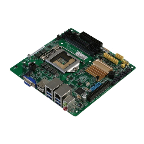
The NT928 P2BXD is a Pentium II based mainboard that utilizes Intel’s
newest 82440BX chipset with in an ATX size. This mainboard is designed for
both Pentium II and Celeron CPU’s It supports new architectures such as
high speed AGP graphic port, Ultra DMA/ 33, Bus Master IDE, SDRAM
memory and is expandable to a maximum of 1Gbyte of memory.
In addition to above features, NT928 P2BXD implements most advanced
technology such as synchronous Switching voltage regulator, CPU thermal
protection, CPU fan monitoring, System voltage monitoring, Over
current protection, Modem Wake Up, Keyboard power on, PS/2 mouse
power on, Debug sensor LED on board and user-friendly jumper-less
CPU speed selection.
The most unique feature of the NT928 P2BXD is its capability to debug
possible installation and peripherals faults onboard. When the CPU, DRAM,
FDD, or VGA cards have not been properly installed, a DIY user can isolate
problems through reading the Debug Sensor LED and instructions in the
manual. To professional system test engineers or maintenance engineers,
the Debug Sensor works as a Port 80 Debug Card for testing and
maintenance in lieu of the 80 Port Debug card.

NT928 P2BXD - User’s Manual
4
Main Features
1. Debug sensor LED display on board.
2. Supports the newest specifications of ACPI.
3. Supports Ultra DMA/33-highest rate IDE transfer speed
4. Supports current CPUs at 66 or 100MHZ clock and future higher speed
CPUs that are compatible with SEC Socket.
5. Support IR/Consumer IR/USB and PS/2 devices.
6. Supports modem ring on.
7. Compatible with PCI 2.1 Spec.
8. With the “power saving” feature, the CPU cooler automatically stops
when the system enters the green mode state.
9. CPU cooling fan connector built in.
10. System fan connector built-in.
11. Supports Intel LDCM Network Manageability.
12. Supports ECC or Non-ECC type SDRAM modules.
13. Supports Keyboard Power On.
14. Supports PS/2 Mouse Power On.
15. Supports BIOS in setting CPU type.
16. Supports automatic closing of the unused DIMM/ PCI clock to
reduce noise.

NT928 P2BXD - User’s Manual
5
CONTENTS
COPYRIGHT ............................................................................ 2
DISCLAIMER............................................................................ 2
OVERVIEW .............................................................................. 3
MAIN FEATURES..................................................................... 4
CONTENTS.............................................................................. 5
INTRODUCTION ...................................................................... 7
A.SPECIFICATIONS ................................................................... 7
SETUP GUIDE ......................................................................... 8
A.LAYOUT DIAGRAM ................................................................. 8
B.SMART DEBUG ON BORAD..................................................... 9
C.CPU VOLTAGE AND FREQUENCIES ...................................... 10
D.EDO/ SDRAM INSTALLATION PROCEDURES: ...................... 12
E.OTHER JUMPER SETTINGS................................................... 15
F.NOTE TO BIOS UPDATE ...................................................... 16
G.KEYBOARD/ PS/2 MOUSE POWER ON AND MODEM RINGON…...17
H.SYSTEM HEALTH MONITOR.................................................. 19
I. EDO/ SDRAM CONFIGURATIONTABLE:............................... 21
AWARD BIOS SETUP............................................................ 23
A.GETTING HELP.................................................................... 24
B.THE MAIN MENU................................................................. 24
1.Standard CMOS Setup.................................................. 25
2.BIOS Features Setup..................................................... 26
3.Chipset Features Setup................................................. 30
4.Power Management....................................................... 34

NT928 P2BXD - User’s Manual
6
5.PNP/PCI Configuration Setup........................................ 36
6.Load BIOS Default......................................................... 38
7.Load Setup Default........................................................ 38
8.Integrated Peripherals Setup......................................... 38
9.Password Setting........................................................... 41
10.IDE HDD Auto Detection.............................................. 42
11.Hard Disk Low Level Format Utility.............................. 42
12.Exiting the Setup Program........................................... 43
TECHNICAL INFORMATION................................................. 44
A.BLOCK DLAGRAM................................................................ 44
B.I/O CONNECTOR MAP ........................................................ 45
C.THE TRANSFER RATE OF IDE PIO AND DMA MODES............. 46
D.THE COMPUTER BOOT FLOW.CHART.................................. 47
E.THE DIFFERENCE OF INTEL 440LX/ EX /BX CHIPSET ................ 48
F.TIME AND DMA CHANNELS MAP.................................... 50
G.INTERRUPT MAP........................................................... 50
H.RTC AND CMOS RAM MAP.............................................. 51
I.POST CODE ....................................................................... 52
J.PROBLEM SHEET................................................................. 57

NT928 P2BXD - User’s Manual
7
Introduction
A. Specifications
System Chipset Intel 82440 BX chipset.
CPU Intel Pentium II processors, support
233/266/300/333 MHz (External Clock 66MHz) .
300/350/400/ 450/ 500 MHz (Ext Clock 100MHz).
Memory Expandable to 768MB (3 banks) with three 168-
pin DIMM sockets {support 3.3 V EDO (66MHz
only) / SDRAM (66MHz/ 100MHz)}.
I/O Winbond 83977, two high speed 16550
compatible serial ports, one Multi-Mode.
Parallel Port support SPP/EPP/ECP standard
mode.
Two onboard PCI IDE ports (32-bit data transfer).
LS-120/ ZIP FDD, IrDA/ ASK IR/ Consumer IR.
Dual USB ports
Supports two 360/720KB/1.2/1.44/2.88MB floppy
disk devices.
One PS/2 Mouse port.
BIOS Award System BIOS installed in socket (Flash and
PnP).
Expansion slots One AGP slot, five PCI Master Slots and two 16-
bit ISA Slots.
Voltage Auto 1.8V-3.5V
Dimension 4-layer PCB, size (300mm x 190mm).
Others CPU speed selection in BIOS (Jumper-less),
CPU Auto Temperature Sensor & Music Alarm,
voltage monitor, CPU Fan and System Fan
monitor, Bus Master/ Ultra DMA/33, ACPI, AGP
Bus, Keyboard Power On, PS/2 Mouse Power On,
Modem Ring On, Lan wake up, Debug sensor on
board.

NT928 P2BXD - User’s Manual
8
Setup Guide
A. Layout Diagram

Technical Information
9
B. Smart Debug On Board
When the CPU module, DRAM, Cache RAM, FDD or VGA cards have not
been properly installed, users can isolate those basic problems through the
Debug Sensor LED and instructions from the manual. For professional
system engineers or maintenance engineers, the Debug Sensor works in the
same fashion as a Port 80 Debug Sensor Card.
NOTE: This is an example of functionality. For detail, see technical section.
Error code Display Message Solution
C1 None Can’t detect
DRAM 1. Re-install or replace the SDRAM.
2. Re-install or replace the BIOS.
C6 None Can’t detect
DRAM 1. Re-install or replace the SDRAM.
2. Re-install or replace the BIOS.
OD None Can’t detect
VGA card 1. Re-install or replace the VGA card.
2. Replace the BIOS.
4E Yes Can’t detect
Floppy disk
1. Replace the BIOS. (if no screen)
2. Enter the BIOS Setup menu to reset.
3. Check that the FDD cable and the power
connector are properly connected.
4. Reconnect the FDD cable or replace the FDD.
61 Yes L2 cache
problem 1. Enter BIOS Setup to disable the external
cache.

NT928 P2BXD - User’s Manual
10
C. CPU Voltage and Frequencies
Before starting, set one jumper, JP1 for external (66/100) clock selection. The ratio
and frequency of the CPU is set up in the BIOS. The corresponding working voltage
for the CPU is automatically detected and set.
Please read carefully the following instructions:
1. Power on the installed system and press the "DEL" key to enter BIOS Setup.
ROM PCI/ISA BIOS (2A69KTJ9)
CHIPSET FEATURE SETUP
AWARD SOFTWARE, INC
Auto Configuration : Enabled Auto Detect DIMM/ PCI Clk : Enabled
EDO DRAM Speed Selection : 60ns CPU Speed : Manual
EDO CASx# MA Wait State : 2 CPU Ratio : X 2.5
EDO RASx# Wait State : 2 CPU Frequency : 100 MHz
SDRAM RAS-to CAS Delay : 3 Spread Spectrum : Disabled
SDRAM RAS Precharge
Time : 3 CPU Warning Temperature : Disabled
SDRAM CAS latency Time : Auto Current CPU Temperature : 28•/ 82•
DRAM Data Integrity Mode : Non-ECC Current SYSFAN Speed :4285 RPM
System BIOS Cacheable : Enabled Current CPUFAN Speed :4000 RPM
Video BIOS Cacheable : Enabled Current Vin3 (V) : 2.88V
Video RAM Cacheable : Disabled
8 Bit I/O Recovery Time : 1
16 Bit I/O Recovery Time : 1
Memory Hole At 15M-16M : Disabled
Passive Release : Enabled Esc : Quit ↑↓→← Selection : Item
Delayed Transaction : Disabled F1 : Help PU/PD/+/- :
Modify
AGP Aperture Size (MB) : 64 F5 : Old Values (Shift) F2 :
Color
F6 : Load BIOS Default
F7 : Load Setup Default
Select "Chipset Features Setup" and press <Enter>.
2. Select "CPU Speed" and press "PgUp" or "PgDn" to set the CPU ratio and
frequency. The available options are:
233MHz (66X3.5), 266MHz (66X4), 300MHz (66X4.5), 333MHz (66X5),
366MHz (66X5.5), 400MHz(66X6), 433MHz(66X6.5), 466MHz(66X7),
500MHz(66X7.5).
250MHz(100X2.5), 300MHz(100X3), 350MHz(100X3.5), 400MHz(100X4),
450MHz(100X4.5), 500MHz(100X5), 550MHz(100X5.5), 600MHz(100X6)
and "Manual".

Technical Information
11
To set the CPU manually, please note the following:
CPU Speed: "Manual" (you can manually set the CPU ratio and frequency)
CPU Ratios: x3.5, x4, x4.5, x5, x5.5, x6, x6.5, x7, x7.5
CPU Frequency: 66, 68, 75, 83, 100, 103, 112, 133Mhz
Several options are provided for the CPU external clock. You are
recommended to restore to the default setting in case of instability when the
external clock exceeds 66MHz.
NOTE: System failure may occur if the CPU frequency is set incorrectly. To
solve this problem, press the "Insert" key on the keyboard to clear the
previously set frequency (i.e., restore the default frequency), and then reboot
the system.
z
Switching voltage is applied, making the temperature lower and voltage
steadier.
z
You don’t need to adjust Voltage in this Pentium II mainboard. It will
automatically send out one VID signal (Voltage Identification) to the
mainboard power supply to ask for the voltage it needs.
z
The CPU type default setting is Intel Pentium II 250MHz=100 MHz•2.5.
(no jumper on JP1)
Intel Pentium II CPU reference
CPU Ext. clk Ratio L1 cache L2 cache Voltage
Intel Pentium II – 500MHz 100MHz X5 32KB 512KB 2.8V
Intel Pentium II – 450MHz 100MHz X4.5 32KB 512KB 2.8V
Intel Pentium II – 400MHz 100MHz X4 32KB 512KB 2.8V
Intel Pentium II – 350MHz 100MHz X3.5 32KB 512KB 2.8V
Intel Pentium II – 300MHz 100MHz X3 32KB 512KB 2.8V
Intel Pentium II – 333MHz 66MHz X5 32KB 512KB 2.8V
Intel Pentium II – 300MHz 66MHz X4.5 32KB 512KB 2.8V
Intel Pentium II – 266MHz 66MHz X4 32KB 512KB 2.8V
Intel Pentium II – 233MHz 66MHz X3.5 32KB 512KB 2.8V

NT928 P2BXD - User’s Manual
12
D. EDO/ SDRAM Installation Procedures:
z
One 168-pin DIMM module can support up to 384MB at either
3.3V EDO (66MHz) or SDRAM (66MHz/ 100MHz).
z
We recommend using SDRAM with Serial Presence Detect that are
compliant with PC-100. This will enable BIOS to detect the SDRAM size,
speed, voltage, its drive strength and number of row/column addresses,
to properly configure it to the system’s performance profile.

Technical Information
13
The following table shows memory modules that have passed the PC-100
specifications.
Brand Memory size Number
TOSHIBA 8M X 08=64MB TC59S6408BFT-80
TOSHIBA 4M X 16=64MB TC59S6416BFT-80
HITACHI 8M X 08=64MB HM5264805TT-B60
HITACHI 4M X 16=64MB HM5264165TT-B60
MITSUBISHI 8M X 08=64MB M5M4V64S30ATP-8
MITSUBISHI 4M X 16=64MB M5M4V64S40ATP-8
MITSUBISHI 2M X 08=16MB M5M4V16S30DTP-8
FUJITSU 8M X 08=64MB 81F64842B-103FN
FUJITSU 4M X 16=64MB 81F641642B-103FN
TI 8M X 08=64MB TMX664814A81A7ET
TI 2M X 08=16MB TMX626812BDGE5M
SAMSUNG 8M X 08=64MB KM48S8030BT-GH
SAMSUNG 4M X 16=64MB KM416S4030BT-G10
SAMSUNG 2M X 08=16MB KM48S2020CT-GL
HYUNDAI 8M X 08=64MB HY57V658020ALTC-10P
HYUNDAI 2M X 08=16MB HY57V168010C TC-10S
LG 8M X 08=64MB GM72V66841CT7J
LG 4M X 16=64MB GM72V661641CT-7J
z
First, verify the working voltage of the EDO/ SDRAM module in either
DIMM socket.
z
This NT928 P2BX only supports 3.3V EDO/ SDRAM modules. The
following illustration shows you the difference between 3.3V and 5V to
ensure your correct selection of 3.3V DIMM module.
z
You can set up the BIOS “Chipset Feature Setup” to the best working
condition based on the type of EDO/ SDRAM you are using.
z
The BIOS DRAM default setting is 60ns. Change the BIOS “Chipset
Feature Setup” default setting to 50ns for better performance, only if
the chips on all modules installed are marked 50ns.

NT928 P2BXD - User’s Manual
14
z
Change nothing in the BIOS if EDO RAM is used. The BIOS
automatically detects the RAM type.
z
MEMO for Installing System:
•Concerning memory setup, you can find out how to from “Chipset
Feature Setup” under BIOS setup. However, to avoid unstable system
operation or system hang, users without engineering background are
not suggested to change BIOS set up, other than CPU speed.
z
The Dual Inline Memory Module (DIMM) must be 3.3 Volt and
Unbuffered Synchronus DRAM (SDRAM) 8MB, 16MB, 32MB or 64MB
The following illustration shows the type of DIMM Module required.
168-PIN SDRAM DIMM Notch Key Definitions
Connector Port Locations

Technical Information
15
E. Other Jumper Settings
Speaker: Connect to the system’s speaker.
z
Keylock: Keyboard lock switch and Power LED connector.
z
Reset: Short to restart system.
z
HDD LED: LED ON lights up when on board PCI IDE hard disk is active.
z
POWER SW (FOR ATX POWER SUPPLY):
The button should be a momentary switch that is normally open.
Pushing the ATX Power Switch will immediately change the system
status. Before or during “POST”, you need to hold the button for four
seconds in order to turn off the system.
z
J19: Clear CMOS
Turn off the system and short pins 2-3 to clear CMOS. Then short pins
1-2 before turning it on.
J19
1-2 Normal operation(Default).
2-3 for clearing CMOS Data.

NT928 P2BXD - User’s Manual
16
z
CPU Cooling Fan connector
This is the connector for CPU cooler. Never use the jumper to short the
connector. Serious damages caused this way will void warranty.
z
Creative SB-Link
It is used to connect the AWE64 or other compatible sound cards so
that they are made compatible with the ISA-compatible SB16 sound
cards.
F. Note to BIOS Update
Do not update the BIOS if no abnormalities occur. However, if BIOS
update is needed, consult your dealer first. Prior to updating your BIOS,
you are recommended to save the original BIOS values.
1. Download the AWARD BIOS Flash Utility file (Awdflash.exe)
2. Download the BIOS file used by your identified mainboard model
(e.g., BXV110N.BIN)
3. Reboot your system (but do not run Himem.sys and Emm386.exe)
to execute the new BIOS program.
4. Execute these commands: Awdflash BXV110N.BIN
5. When this message displays: "Do you want to save BIOS (Y/N)?"
Type "N"
6. When this message displays: "Are you sure to program (Y/N)?"
Type "Y"
7. Turn off power to your system to clear the CMOS data.
8. Turn on the power to test if your system is running normal.

Technical Information
17
G. Keyboard/ PS/2 Mouse Power On and MODEM Ring on
z
Make sure your ATX Power Supply can provide the full strength 5V
SB-signal required, which is nearly 750mA (Amperage). Your ATX
Power Supply should be able to supply at least 1 Ampere.
z
If you are going to use the function of keyboard and PS/2 mouse
power on, the power-switch will be become disabled
automatically. ROM PC/ISA BIOS (2A69KTJ9)
INTEGRATED PERIPHERALS
AWARD SOFTWARE, INC.
IDE HDD Block Mode : Enabled Onboard Serial Port 2 : 2F8H / IRQ3
IDE Primary Master PIO : AUTO UART Mode Select : Normal
IDE Primary Slave PIO : AUTO
IDE Secondary Master PIO : AUTO Onboard Parallel Port : 378H/IRQ 7
IDE Secondary Slave PIO : AUTO Parallel Port Mode : ECP+EPP
IDE Primary Master UDMA : AUTO ECP Mode Use DMA : 3
IDE Primary Slave UDMA : AUTO EPP Mode Select : EPP 1.9
IDE Secondary Master
UDMA : AUTO
IDE Secondary Slave
UDMA : AUTO
On-Chip Primary PCI IDE : Enabled
On-Chip Secondary PCI IDE : Enabled
USB Keyboard Support : Disabled
Init AGP Display First : Enabled
POWER ON Function : Hot KEY Esc : Quit ↑↓→← Selection : Item
Hot Key Power ON : Ctrl-F12 F1 : Help PU/PD/+/- : Modify
KBC input clock : 8MHz F5 : Old Values (Shift)F2 : Color
Onboard FDC Controller : Enabled F6 : Load BIOS Default
Onboard Serial Port 1 : 3F8H / IRQ4 F7 : Load Setup Default
Hot KEY Selection of this option will allow setting another function
key as Hot Key Power ON:
Ctrl-F(1/2/3/4/5/6/7/8/9/10/11/12) selects any one.
After power is turned off, when user keys in the "Ctrl-F?",
it will power on the system.
PS/2 Mouse Left Will power on the system by PS/2 mouse left.
PS/2 Mouse Right Will power on the system by PS/2 mouse Right.
Button Only Only the power button can power on the system.

NT928 P2BXD - User’s Manual
18
z
Modem Ring On Function Operation:
ROM PCI / ISA BIOS (2A69KTJ9)
POWER MANAGEMENT SETUP
AWARD SOFTWARE, INC
Power Management : Disabled ** Reload Global Timer Events **
PM Control by APM : No IRQ[3-7, 9-15], NMI : Enabled
Video Off Method : V/H
SYNC+Blank Primary IDE 0 :
Disabled
Video Off After : Standby Primary IDE 1 :
Disabled
MODEM Use IRQ : 3 Secondary IDE 0 :
Disabled
Doze Mode : Disabled Secondary IDE 1 :
Disabled
Standby Mode : Disabled Floppy Disk :
Disabled
Suspend Mode : Disabled Serial Port : Enabled
HDD Power Down : Disabled Parallel Port :
Disabled
Throttle Duty Cycle : 62.5%
ZZ Active in Suspend : Disabled
VGA Active Monitor : Enabled
Soft-Off by PWR-BTTN : Instant-Off
CPUFAN Off In Suspend : Enabled
Resume by Ring : Enabled
IRQ 8 Clock Event : Disabled Esc : Quit ↑↓→←Selection Item
F1 : Help PU/PD/+/- : Modify
F5 : Old Values (Shift) F2 : Color
F6 : Load BIOS Default
F7 : Load Setup Default
1. Have an external MODEM connected to COM 1 or COM 2.
2. Enter BIOS setup.
3. Select Power Management Setup.
4. This number of MODEM Use IRQ has to be set the same as the IRQ of the
Serial Port to which the modem is connected. Please set to N/A if you are
not going to use the function of MODEM ring on.
5. Resume by Ring: Enable.
6. Save BIOS setup and Reboot.
7. Booting from DOS, Windows, or Windows 95.
8. Turn off the system by:
a. ATX-Power Switch
b. Windows 95 Software Power Off
9. System Waiting for Modem Ring On
When Modem Ringing Signal Active, System will wake-up.

Technical Information
19
H. System Health Monitor
This software is supplied on disk.
z
Fan Monitoring:
The NT928 BXD provides for two fan connectors, one is for the CPU,
the other for an additional housing fan. When the fan’s speed is working
abnormally, there will be a warning (Speaker Alarm) issued through
application software such as SM10 (Small Icon for System Monitoring)
to notify user. The fan monitoring function is implemented by connecting
fan to 3-pin fan connector FAN1/ FAN2 and installing SM10 software.
Refer to Page 16 for jumper selection (System Health Monitor).

NT928 P2BXD - User’s Manual
20
z
CPU Thermal Protection:
The NT928 P2BXD implements special thermal protection circuits.
When temperature is higher than a predefined value, there will be
warning (Speaker Alarm) through application software such as SM10
(Small Icon for System Monitor) to notify user. It is implemented
automatically by BIOS or SM10, no hardware installation is needed.
Refer to Page16 (System Health Monitor).
This mainboard also provides an option to use a CPU cooling fan with
Thermal Sensor on it. The CPU thermal sensor should be connected to
J16.
z
System Voltage Monitoring:
NT928 P2BXD is featured with a voltage monitoring system. When you
turn on your system, this smart design will keep on monitoring your
system working voltage. If any of the required voltage is abnormal to a
component's standard, there will be Speaker Alarm though application
software SM10 (Small Icon For System Monitor) for a warning to user.
System voltage monitoring function monitors 5V, 12V, 3.3V and CPU
voltage. It is implemented automatically by BIOS and SM10, no
hardware installation is needed. Refer to Page 19 (System Health
Monitor)
Table of contents
