Nuvoton NAU88L21 User manual

Feb 28, 2022 Page 1 of 78 Rev 2.8
NAU88L21
Ultra-Low Power Audio CODEC Ground-Referenced Headphone Amplifier
GENERAL DESCRIPTION
The NAU88L21 is an ultra-low power high performance audio codec that supports both analog and digital audio functions. It includes
one I2S/PCM interface, one digital microphone interface, one digital mixer, two high quality DACs and ADC’s, and one stereo class
G headphone amplifier. The advanced on-chip signal processing engine that includes dynamic range compressor (DRC),
programmable biquad filter, as well as an integrated frequency locked loop (FLL) to support various input clocks.
FEATURES
DAC: 105dB SNR, (A-weighted) @ 0dB gain, 1.8V and -
88dB THD @ 20mW and RL= 32Ω, DAC playback to
headphone output mode
ADC: 103dB SNR (A-weighted) @ 0dB MIC gain, 1.8V, Fs
= 48kHz and -93dB THD, 1.8V, MIC gain 0dB, OSR 256x
1 Digital I2S/PCM I/O port
Two mono differential or one stereo differential analog
microphone inputs, two single-ended microphone inputs or
one stereo digital microphone input
Cap-free Low noise Microphone bias with 7uVrms noise
between 20Hz-20kHz, internal pull high resistor for
microphone.
Class G Headphone Amplifier (28mW @ 32Ω, 1%
THD+N)
Sampling rate from 8k to 192 kHz
Dynamic Range Compressor (DRC)Programmable Biquad
filter Integrated DSP with specific functions:Input
automatic level control (ALC/AGC)/limiter
Output dynamic-range-compressor/limiter
Package: 32 Pin QFN package
APPLICATIONS
Gaming controller
Wireless Headset
Smart Remote Controller

Feb 28, 2022 Page 2 of 78 Rev 2.8
Block Diagram - QFN32
Charge
Pump
ADC
MICBIAS
FLL
MUX
ADC Effect
Volume
DRC
Programmable
BiQuad
Interface
& MUX
DAC Effect
Volume
DRC
Programmable
BiQuad
BCLK
FS
DAC HPL
CPOUTP
VSSCP
CPCB
CPOUTN
CPCA
Digital Audio
Effects
Mixers
Sidetone
I2S/PCM
DAC HPR
MICBIAS
I2 C Slave
& Registers
MICL+
BIAS
VREF
SCLK
SDIO
DACIN
ADCOUT
GPIO1
VDDA
VDDB
VSSD
VDDA(2)
VSSA
VDDMIC
MCLK
ADC
MICR+
MUX MUX
DMIC I/F
MICR-
MICL -
MICDET
MICDET
GPIO2

Feb 28, 2022 Page 3 of 78 Rev 2.8
Table of Contents
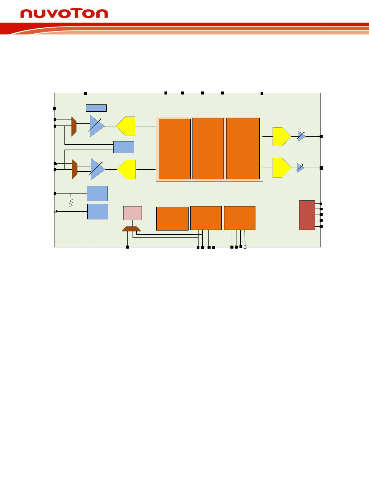
BLOCK DIAGRAM - QFN32...................................................................... 2
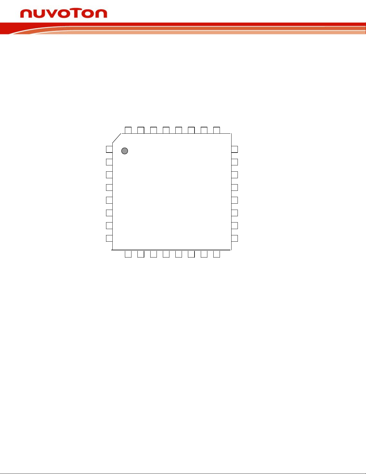
PIN DIAGRAM........................................................................................... 6
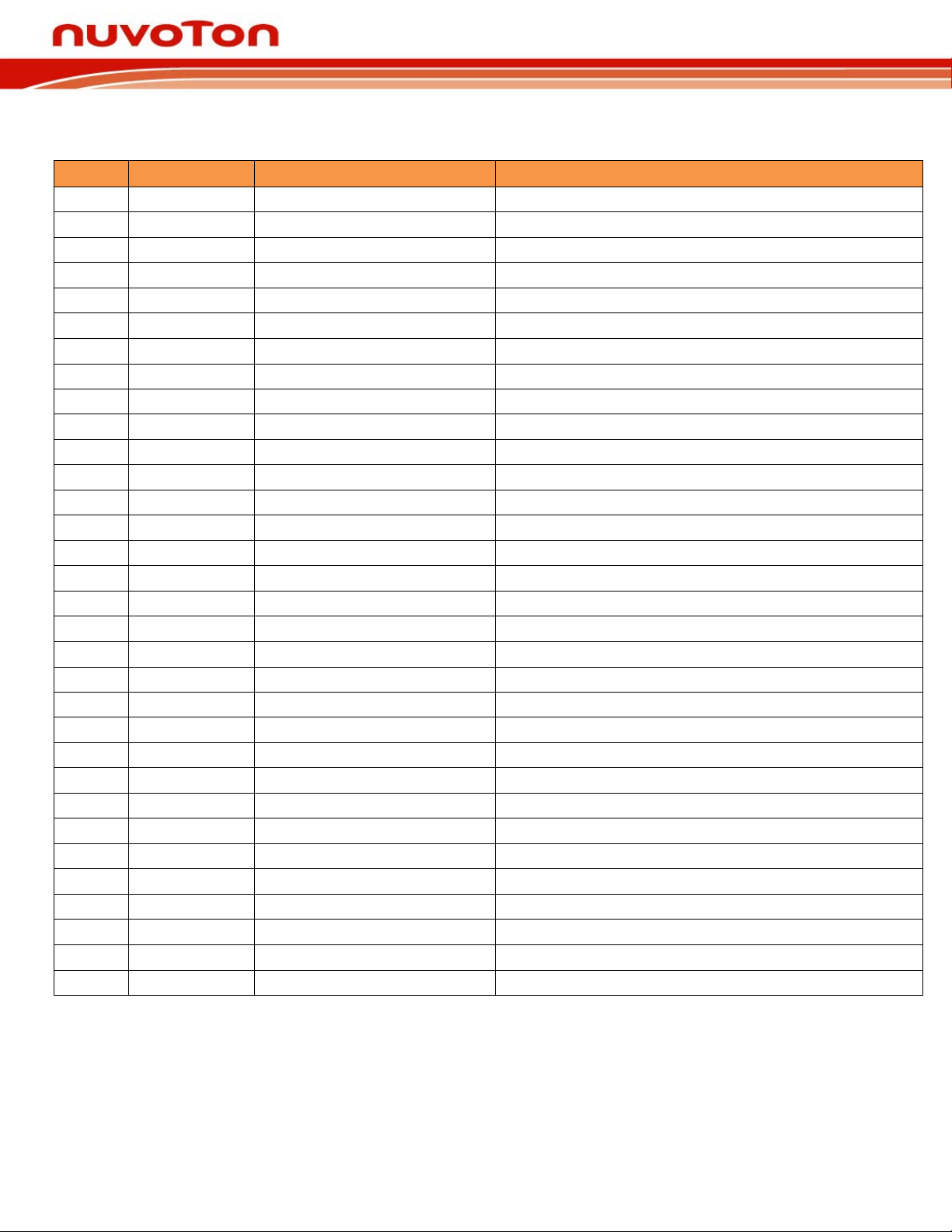
PIN DESCRIPTION.................................................................................... 7
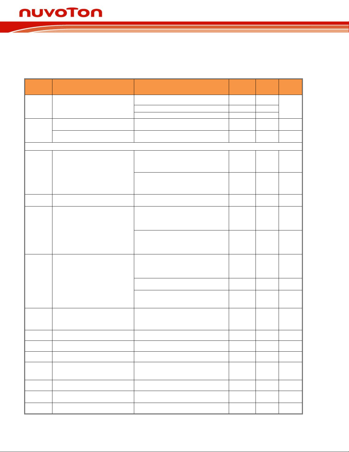
ELECTRICAL CHARACTERISTICS.......................................................... 8
1. GENERAL DESCRIPTION................................................................ 11
1.1 Inputs............................................................................................................... 11
1.2 Outputs............................................................................................................ 11
1.3 ADC, DAC and Digital Signal Processing........................................................ 11
1.4 Digital Interfaces.............................................................................................. 11
2. POWER SUPPLY ............................................................................. 12
2.1 Power on and off reset..................................................................................... 12
2.2 Power up and Start Sequence......................................................................... 12
3. INPUT PATH DETAILED DESCRIPTIONS....................................... 13
3.1 Analog Microphone Inputs............................................................................... 13
3.2 Digital Microphone Input.................................................................................. 14
3.3 VREF............................................................................................................... 14
3.4 MIC Bias.......................................................................................................... 15
3.5 MIC detect....................................................................................................... 15
3.5.1 Key Release .......................................................................................................................................17
4. ADC DIGITAL BLOCK...................................................................... 18
4.1 ADC Dynamic Range Compressors (DRC) ..................................................... 18
4.1.1 Level Estimation .................................................................................................................................18
4.1.2 Static Curve........................................................................................................................................18
4.1.3 Limitation ............................................................................................................................................20
4.2 ADC Digital Volume Control ............................................................................ 21
4.3 ADC Programmable Biquad Filter ................................................................... 21
4.4 Companding.................................................................................................... 22
4.5 Additional ADC Application Notes ................................................................... 22
5. DAC DIGITAL BLOCK...................................................................... 23
5.1 DAC Dynamic Range Control (DRC)............................................................... 23
5.1.1 Level Estimation .................................................................................................................................23
5.1.2 Static Curve........................................................................................................................................24
5.2 DAC Digital Volume Control, Mute and Channel selection.............................. 25
5.3 DAC Soft Mute................................................................................................. 25
5.4 DAC Auto Attenuate ........................................................................................ 25
5.5 DAC Path Digital Mixer with Side tone............................................................. 25

Feb 28, 2022 Page 4 of 78 Rev 2.8
5.6 Companding.................................................................................................... 27
5.6.1 µ-law...................................................................................................................................................27
5.6.2 A-law...................................................................................................................................................27
6. CLOCKING AND SAMPLE RATES.................................................. 28
6.1 I2S/PCM Clock Generation.............................................................................. 29
6.2 Frequency Locked Loop(FLL).......................................................................... 31
7. CONTROL INTERFACES................................................................. 33
7.1 2-Wire-Serial Control Mode (I2C Style Interface)............................................. 33
7.2 2-Wire Protocol Convention............................................................................. 33
7.3 2-Wire Write Operation.................................................................................... 34
7.4 2-Wire Read Operation.................................................................................... 35
7.5 Digital Serial Interface Timing.......................................................................... 36
Table 13 Digital Serial Interface Timing Parameters................................................. 36
7.6 Software Reset................................................................................................ 36
8. DIGITAL AUDIO INTERFACES........................................................ 37
8.1 Digital Audio Interface...................................................................................... 37
8.1.1 Right-Justified Audio Data............................................................................... 37
8.1.2 Left-Justified Audio Data.................................................................................. 37
8.1.3 I2S Audio Data ................................................................................................ 37
8.1.4 PCMA Audio Data ........................................................................................... 38
8.1.5 PCMB Audio Data ........................................................................................... 38
8.1.6 PCM Time Slot Audio Data.............................................................................. 38
8.1.7 TDM I2S Audio Data........................................................................................ 39
8.1.8 TDM PCMA Audio Data................................................................................... 39
8.1.9 TDM PCMB Audio Data................................................................................... 40
8.1.10 TDM PCM Offset Audio Data...................................................................... 40
8.2 Digital Audio Interface Timing Diagrams.......................................................... 42
8.2.1 Digital Audio Interface Slave Mode.................................................................. 42
8.2.2 Digital Audio Interface Master Mode................................................................ 43
8.2.3 PCM Audio Interface Slave Mode.................................................................... 44
8.2.4 PCM Audio Interface Master Mode.................................................................. 44
8.2.5 PCM Time Slot Audio Interface Slave Mode.................................................... 45
8.2.6 PCM Time Slot Audio Interface Master Mode.................................................. 45
9. OUTPUTS......................................................................................... 46
9.1 Class G Headphone Driver and Charge Pump................................................ 46
10. CONTROL AND STATUS REGISTERS ........................................... 47
11. TYPICAL APPLICATION DIAGRAM................................................ 72

Feb 28, 2022 Page 5 of 78 Rev 2.8
12. PACKAGE INFORMATION .............................................................. 73
13. REVISION HISTORY ........................................................................ 77
IMPORTANT NOTICE............................................................................ 78

Feb 28, 2022 Page 6 of 78 Rev 2.8
Pin Diagram
QFN 32-pin
26
25
28
27
30
29
31
32
20
24
18
17
22
23
19
21
16
14
15
12
13
10
11
9
1
2
3
4
6
7
8
5
MCLK
DACIN
CPOUTN
VDDA
HPOUTR
HPOUTL
CPCA
CPCB
VSSA
VREF
VDDMIC
VDDA
HPFB
VDDB
SCLK
SDIO
IRQ
GPIO2/JKDET
BITCLK
CPOUTP
MICL+
MICBIAS
VSSD
VDDA
ADCOUT
MICL-/DMICDATA
FS
GPIO1/CSB
VSSCP
MICDET
MIC R -/DMICCLK
MIC R +

Feb 28, 2022 Page 7 of 78 Rev 2.8
Pin Description
Pin # Name Type Functionality
1 MICDET Analog IO Microphone/button detect, 2kOhm between Mic and Mic Bias
2 MICBIAS Analog Output Microphone Bias Output
3 VDDMIC Supply Microphone supply
4 VREF Analog I/O Internal DAC & ADC voltage reference decoupling I/O
5 VSSA Ground Analog Ground
6 VDDA Supply Analog Supply
7 CPOUTP Analog I/O Charge Pump positive voltage
8 VSSCP Ground Charge Pump Supply ground
9 CPOUTN Analog I/O Charge Pump negative voltage
10 CPCB Analog I/O Charge Pump switching capacitor node B
11 CPCA Analog I/O Charge Pump switching capacitor node A
12 JKTIP(HPL) Analog Output Jack Tip; Headphone left channel output
13 JKR1(HPR) Analog Output Jack Ring1; Headphone right channel output
14 HPFB Ground Headphone Ground
15 IRQ Digital I/O IRQ
16 GPIO1/CSB Digital I/O General Purpose IO/CSB
17 SDIO Digital I/O Serial Data for I2C
18 SCLK Digital Input Serial Data Clock for I2C
19 VDDB Supply Digital IO Supply
20 VSSD Ground Digital IO ground
21 VDDA Supply Analog supply
22 MCLK Digital Input CODEC Master clock input
23 BCLK Digital I/O Serial data bit clock input or output for I2S or PCM data
24 FS Digital I/O Frame Sync input or output for I2S or PCM data
25 DACIN Digital Input Serial Audio data input for I2S or PCM data
26 ADCOUT Digital Output Serial Audio data Output for I2S or PCM data
27 JKDET Analog Input Jack detect input
28 MICR+ Analog Input PGA MICR+ Analog Input
29 MICR-/DMCLK Analog/Digital Output PGA MICR- Analog Input / Digital Microphone Clk output
30 MICL-/DMDATA Analog Input/Digital Input PGA MICL- Analog Input / Digital Microphone Data input
31 MICL+ Analog Input PGA MICL+ Analog Input
32 VDDA Supply Analog Supply

Feb 28, 2022 Page 8 of 78 Rev 2.8
Electrical Characteristics
Conditions: VDDA = VDDB = 1.8V; VDDMIC= 3.6V.
RL(Headphone) = 32 Ω, f = 1kHz, MCLK=12.88MHz, unless otherwise specified. Limits apply for TA= 25°C
Symbol Parameter Conditions Typical Limit Units
ISD Shutdown Current
V
DD
A
4
16
µA
V
DD
B
0.2
1
VDDMIC
0.2
1
IDD
Headset Detection Standby
Mode
MCLK off, Jack Insertion, IRQ enabled 10 µA
Active Current Normal Playback
Mode
f
S
= 48kHz, Stereo HP DAC On, HP
On, POUT = 0mW. RL(HP) = 32Ω
5 mA
Headphone Amplifier
POOutput Power
Stereo RL = 32Ω, DAC Input, CPVVDD =
1.8V, f=1020Hz, 22kHz BW,
THD+N = 1% (QFN package), 28 mW
Stereo RL = 16Ω, DAC Input, CPVVDD =
1.8V, f=1020Hz, 22kHz BW,
THD+N = 1% (QFN Package)
33 mW
THD+N
Total Harmonic Distortion +
Noise
RL = 32Ω, f=1020Hz, PO= 20mW -88 dB
SNR Signal to Noise Ratio
VOUT = 1VRMS, DAC Input,
DAC_Gain = 0dB, HP_Gain = 0dB,
Digital Zero Input, f=1020Hz, A-
Weighted)
105 dB
VOUT = 1 V
RMS
, DAC Input,
DAC_Gain = 0dB, HP_Gain = 0dB,
Digital Zero Input, f=1020Hz, A-
Weighted, auto attenuate enabled,
108 dB
PSRR Power Supply Rejection Ratio
f
RIPPLE
= 217Hz, V
RIPPLE
= 200mV
P_P
Input Referred, HP_GAIN = 0dB
DAC Input, DAC_Gain = 0dB Ripple
Applied to VDDA
90 dB
Mono_Gain = 0dB Ripple Applied to
VDDA
90 dB
Stereo Single Ended Input Terminated,
Stereo_Gain = 0dB Ripple Applied
to VDDA
90 dB
XTALK Channel Crosstalk Left Channel to Right Channel, -
1dBFS, Gain = 0dB, f
= 1020Hz
70 dB
Interchannel Level Mismatch +/- 0.1 dB
Frequency Response F = 20Hz ~ 20kHz +0.1/-0.2 dB
Pop up Noise 1 mVrms
eOS Output Noise
DAC_Gain = 0dB, HP_Gain = 0dB,
fS=48kHz, OSRDAC = 128, A-
Weighted
4.4 uVRMS
Out of Band Noise Level -60dB
VOS Output Offset Voltage
HP_Gain = 0dB, DAC_Gain= 0dB,
DAC Input
±1 mV
Power Consunption MP3 Mode No Load, No Signal, Amp on 6 mW

Feb 28, 2022 Page 9 of 78 Rev 2.8
Symbol Parameter Conditions Typical Limit Units
f
S
= 48kHz, Stereo DAC On, Amp On,
POUT = 0mW. RL = 32Ω
Fs Accuracy (44.1 / 48 kHz)
+/-
0.02%
Pop and Click Noise plug Into or out of DAC to Headphone 1 mVrms
ADC
THD+N ADC Total Harmonic Distortion +
Noise
MIC Input, MIC_GAIN = 0dB, VIN =
0.8Vrms, f=1020Hz, fs = 48KHz,
Mono Differential Input
-91 dB
MIC Input, MIC_GAIN = 30dB, Volume
= 0dB, Vin=28.5mVrms, f=1020Hz,
Digital Gain = 0dB, Mono
Differential Input
-80 dB
SNR Signal to Noise Ratio
Reference = VOUT(0dBFS), A-
Weighted, MIC Input, MIC Gain =
0dB,fs = 48kHz, Mono Differential
Input
102 dB
Reference = VOUT(0dBFS), A-
Weighted, MIC Input, MIC Gain =
6dB,fs = 48kHz, Mono Differential
Input
101 dB
PSRR Power Supply Rejection Ratio
V
RIPPLE
= 200mV
PP
applied to V
DD
A,
fRIPPLE = 217Hz, Input Referred,
MIC_GAIN = 0dB Differential Input
90 dB
CMRR Common Mode Rejection Ratio Differential Input 100mVrms, PGA gain
= 20dB, frequency sweep from
20Hz to 20KHz 65 dB
FSADC
ADC Full Scale Input Level
VDDA= 1.8V
1
VRMS
Minimum Input Impedance 10 kOhm
Frequency Response f = 20Hz ~ 20kHz +0.1/-0.2 dB
Pop up Noise TBD 1 mVrms
Power Consumption
No Signal, ADC on
fs= 44.1kHz
5 mW
MICBIAS
VBIAS Output Voltage Programmable 1.8V to 3.0V in 6 steps 2.5 V
I
OUT
Output Current
4
mA
eos Output Noise Low noise mode, at 1kHz 47 nV/√Hz
Digital I/O
Parameter
Symbol
Comments/Conditions
Min
Max
Units
Input LOW level VIL
VDDB = 1.8V
0.33*VDDB
V
VDDB = 3.3V
0.37*VDDB
Input HIGH level VIH
VDDB = 1.8V
0.67*VDDB
V
VDDB = 3.3V
0.63*VDDB
Output HIGH level VOH ILoad= 1mA
VDDB=1.8V
0.9*VDDB
V
VDDB = 3.3V
0.95*VDDB
Output LOW level VOL ILoad= 1mA
VDDB = 1.8V
0.1*VDDB
V
VDDB=3.3V
0.05*VDDB

Feb 28, 2022 Page 10 of 78 Rev 2.8
Recommended Operating Conditions
Condition Symbol Min Typical Max Units
Digital I/O Supply Range
VDDB
1.62
3.3
3.6
V
Analog Supply Range
VDDA
1.62
1.8
1.98
V
Headphone Supply Range
VDDA
1.62
1.8
1.98
V
Microphone Bias Supply Voltage
VDDMIC
3.0
3.3
3.6
V
Temperature Range
TA
-40
+85
°C
Absolute Maximum Ratings
Parameter Min Max Units
Digital Supply Range
-0.3
2.2
V
Digital I/O Supply Range
-0.3
4.0
V
Analog Supply Range
-0.3
2.2
V
Headphone Supply Range
-0.3
2.2
V
Microphone Bias Supply Voltage
-0.3
4.0
V
Voltage Input Digital Range
DGND - 0.3
VDD + 0.3
V
Voltage Input Analog Range
AGND - 0.3
VDD + 0.3
V
Junction Temperature, TJ
-40
+150
°C
Storage Temperature
-65
+150
°C
CAUTION: Do not operate at or near the maximum ratings listed for extended periods. Exposure to such conditions may adversely
influence product reliability and result in failures not covered by warranty.

Feb 28, 2022 Page 11 of 78 Rev 2.8
1. General Description
NAU88L21 is an ultra-low power CODECs that has both analog and digital blocks operating at 1.8V. This CODEC
includes DSP functions including DRCs (Dynamic Range Compression) and programmable biquad filters. Mic bias
supply is upgraded to support voltages up to 3V.
1.1 Inputs
The NAU88L21 provides analog inputs to acquire and process audio signals from microphones with high fidelity and
flexibility. There is a stereo input path that can be used to capture signals from single-ended or differential sources.
The channel has a fully differential programmable gain amplifier (PGA). The outputs of the PGA connect to the ADC.
The NAU88L21 also has an input for one digital microphone. The NAU88L21 provides a DMCLK, the clock signal for
the digital microphones.
The analog and the digital microphone inputs cannot be used simultaneously.
1.2 Outputs
NAU88L21 has one pair of ground-referenced Class G headphone outputs that are fed by two DACs. The headphone
amplifier has a gain range of -9dB to 0dB.
The Class G headphone amplifier is powered by the charge pump output voltages CPOUTP and CPOUTN. When
there is no loading the CPOUTP is equal to VDDA, and CPOUTN is equal to –VDDA.
This headphone output can also be used as a lineout.
1.3 ADC, DAC and Digital Signal Processing
The NAU88L21 has two independent high quality ADC’s and DACs. These are high performance 24-bit sigma-delta
converters, which are suitable for a very wide range of applications.
The ADCs and DACs have functions that individually support digital mixing and routing. The ADCs and DACs blocks
also support advanced digital signal processing subsystems that enable a very wide range of programmable signal
conditioning and signal optimizing functions. All digital processing is done with 24-bit precision to minimize processing
artifacts and maximize the audio dynamic range supported by the NAU88L21.
The ADCs and DACs digital signal process can support two-point dynamic range compressors (DRCs), programmable
biquad filters configurable for low pass filters, high pass filters, Notch filter, Bell, low shelf, and high shelf filters with
various gain, Q, and frequency controls. Two-point DRCs can be programmed to limit the maximum output level and/or
boost a low output level. The biquad filters can be configured as high pass filters intended for DC-blocking or low
frequency noise reduction, such as reducing unwanted ambient noise or “wind noise” on a microphone inputs.
1.4 Digital Interfaces
Command and control of the device is accomplished by using the I2C interface.
The digital audio I/O data streams transfer separately from command and control using either I2S or PCM audio data
protocols
These simple but highly flexible interface protocols are compatible with most commonly used serial data protocols, host
drivers, and industry standard I2S and PCM devices.

Feb 28, 2022 Page 12 of 78 Rev 2.8
2. Power Supply
This NAU88L21 has been designed to operate reliably using a wide range of power supply conditions and power-
on/power-off sequences. Because of this, there are no special requirements for the sequence or rate at which the
various power supply pins change. Any supply can rise or fall at any time without harming the device. However, pops
and clicks may result from some sequences.
2.1 Power on and off reset
The NAU88L21 includes a power on reset circuit on chip. The circuit resets the internal logic control at VDDA supply
power up and this reset function is automatically generated internally when power supplies are too low for reliable
operation. The reset threshold is approximately 0.55Vdc and 1.0Vdc for VDDA. It should be noted that these values
are much lower than the required voltage for normal operation of the chip.
The reset is held on while the power levels for VDDA are below their respective thresholds. Once the power levels rise
above their thresholds, the reset is released. Once the reset is released, the registers are ready to be written to. It is
also important to note that all the registers should be kept in their reset state for at least 6µs.
An additional internal RC filter based circuit is added which helps the circuit respond for fast ramp rates (~10µs) and
generate the desired reset period width (~10µs at typical corner). This filter is also used to eliminate supply glitches
which can generate a false reset condition, typically 50ns.
For reliable operation, it is recommended to write any value to register upon power up. This will reset all registers to the
known default state.
Note that when VDDA are below the power on reset threshold, then the digital IO pins will go into a tri-state condition.
2.2 Power up and Start Sequence
The power up sequence to bring up the analog blocks smoothly is illustrated below and involves three different time
segments (T1 – T4). The power supply ramp rate depends on a number of factors such as the power source drive
strength, board parasitics and the decopling capacitor size on the supply line. Typically, a power supply ramp time can
be as fast as 5mS or as slow as 200mS.
During time T1, the power supply ramps-up. The internal PORB reset is generated when VDDA is lower than 1.1V for
reliable maintenance of internal logic circuits. While PORB signal is low, it clears internal digital flops. Most of the flops
will be cleared to ‘0’ while some flops can be set to ‘1’ during the PORB pulse depending on the required default state of
the register.
After time T1, wait another time 1mS so that the power supply is stable before writing to the registers. During time T2,
the chip is in stand-by mode and all registers are in a default state. In stand-by, the chip only consumes leakage
current and all analog blocks are turned-off. At time T3, the user can start to write data into the registers via the I2C
serial bus to setup the chip for their application.
When I2C finished loading register in T3 period, waiting for T4, 1ms period, I2S clocks could input to device.

Feb 28, 2022 Page 13 of 78 Rev 2.8
VDDA/VDDB
I2C
T2=1ms
1ms
I2S Clock
MCLK/BCLK/Fs/DATA
T1=5ms~200ms
T2
PORB
`
T4
T1 T3
T4=1ms
Figure 1: Power up sequence
3. Input Path Detailed Descriptions
NAU88L21 has two low noise, high common mode rejection ratio analog microphone differential input. The microphone
inputs MICL+/- & MICR+/- which are followed by -1dB to 36dB PGA gain stages that have a fixed 12kOhm input
impedance.
Inputs are maintained at a DC bias of approximately ½ of the VDDA supply voltage. Connections to these inputs
should be AC-coupled by means of external DC blocking capacitors suitable for the device application.
The differential microphone input structure is essential in noisy digital systems where amplification of low-amplitude
analog signals is necessary such as in portable digital media devices and cell phones. Differential inputs are also
very useful to reduce ground noise in systems in which there are ground voltage differences between different chips
and components. When properly implemented, the differential input architecture offers an improved power-supply
rejection ratio (PSRR) and higher ground noise immunity.
3.1 Analog Microphone Inputs
The analog microphone inputs are routed to the FEPGA (Front End Programmable Gain Amplifier). The input stage
can be configured in different modes. The FEPGA gain can be varied from -1dB to 36dB in 1dB steps. The gain stage
has a fixed 12kOhm input impedance and can be individually enabled or disabled by using register.
As shown in Figure 1,
For left channel input path
SL1, it is controlled by 0x76[11]DISCHRG and 0x77[14]ACDC_CTRL[0],
SL2, it is controlled by 0x76[11]DISCHRG and 0x77[15]ACDC_CTRL[1],
SL3 and SL4, they are controlled by 0x77[5]FEPGA_MODEL[1],
SL5 and SL6, they are controlled by 0x77[7]FEPGA_MODEL[3],
For right channel input path
SR1, it is controlled by 0x76[11]DISCHRG and 0x77[14]ACDC_CTRL[0],
SR2, it is controlled by 0x76[11]DISCHRG and 0x77[15]ACDC_CTRL[1],

Feb 28, 2022 Page 14 of 78 Rev 2.8
SR3 and SR4, they are controlled by 0x77[1]FEPGA_MODER[1],
SR5 and SR6, they are controlled by 0x77[3]FEPGA_MODER[3].
AUXL
-
AUXL
+
]
VREF
AUXR
-
AUXR+
VREF
DMIC
Interface
0 to 36 dB
1 dB Steps
0 to 36dB
1dB Steps
MICL-
DMSELECT
ADCDATA
muteL
muteR
To Left
Audio
ADC
To Right
Audio
ADC
To decimators
FEPGA_MODEL[0]
]
FEPGA
_MODER[0]
PGA _GAINR[5:0]
PGA _GAINR[5:0]
FEPGA_MODER[0]
MICL+
MICR-
MICR+
FEPGA_MODEL[0]
PGA_GAINL[5:0]
PGA_GAINL[5:0]
SL2
SR2
SL1
SL3
SL4
SR5
SL5
SL6
SR6
SR1
SR4
S3
0x77[14]&0x76[11]
0x77[14]&0x76[11]
0x77[15]&0x76[11]
0x77[15]&0x76[11]
0x77[5]
0x77[5]
0x77[7]
0x77[7]
0x77[1]
0x77[1]
0x77[3]
0x77[3]
Figure 2: Microphone Input Block Diagram with Registers
3.2 Digital Microphone Input
The MICL- and MICR- pins can be used for the digital microphone input. MICR- is the clock for the digital microphones
and the MICL- is the data in.
3.3 VREF
The NAU88L21 includes a mid-supply reference circuit that produces a voltage close to VDDA/2. This “VREF” pin
should be decoupled to VSS through an external bypass capacitor. Because VREF is used as a reference voltage
inside the NAU88L21, a large capacitance is required to achieve good power supply rejection at low frequency.
Typically, a value of 4.7µF should be used. This larger capacitance may introduce longer rise time of VREF and delay
the line output signal. However, a pre-charge circuit can be supported to help reduce the rise time. Due to the high
impedance of the VREF pin, it is important to use a low leakage capacitor. A pre-charge circuit has been implemented
to reduce the VREF rise time. Once charged, this can be disabled using to save power or prevent rapid changes in
level due to fluctuations in VDDA. The below Table 1 shows the VREF tie-off resister selection.

Feb 28, 2022 Page 15 of 78 Rev 2.8
VMIDSEL
VREF Resistor Selection
VREF Impedance
00
Open, no resistor selected
Open, no impedance installed
01
50kOhm
25kOhm
10
250kOhm
125kOhm
11
5kOhm
2.5kOhm
Table 1: VREF Impedance Selection
VMIDEN
VDDA Pin
VREF Pin
VSSA Pin
4.7µF
Pre-Charge
VMIDSEL
5, 50, 250 kΩ
PDVMDFST
Register: BIAS_ADJ
Register: BOOST
Exterior
Connections
Figure 3: VREF Circuitry
3.4 MIC Bias
The NAU88L21 provides one MIC bias pin, which can be used to power various microphones. The output level of MIC
Bias can be set between VDDA and 1.53 X VDDA using register settings.
It is recommended that the microphones do not draw more than 4mA from the MICBIAS pin. There are options for
connecting internal 2 Kohm resistor to the microphone and for low noise or low power mode. If MICBIAS is used in low
power mode, typically 100nF or 200nF capacitor can be used along with MIC Bias level at VDDA. In the low noise
mode, external 1uF or 4.7uF capacitor can be omitted by register settings when MIC Bias is used to power analog
microphones.
3.5 MIC detect
The MIC detect block can detect whether a microphone is connected between the MICBIAS output and the MICDET
pin. Either the internal 2kOhm resistor or an external 2kOhm resistor can be used to connect the microphone to the
MICDET pin and MICBIAS. See Figure 4, where the internal hookup of the MICDET and MICBIAS blocks is shown.

Feb 28, 2022 Page 16 of 78 Rev 2.8
MICBIAS
MICDET
Button Detect
Mic Detect
MicBias
MicDet
Figure 4. Mic Detect and MICBIAS blocks
Application note: Adding a simple RC on the MICDET pin can help reduce noise coupling. These may be board level
related, or component related effects.
Figure 5. Reducing noise coupling effects
If the optional external 2KOhm resistor is used, then the internal 2K Ohm resistor (Between MICBIAS and MICDET)
should be disabled.

Feb 28, 2022 Page 17 of 78 Rev 2.8
3.5.1 Key Release
This feature detects the edge case where the key press interrupt is not followed by a release interrupt until later on in
the sequence and clears the x11 register to prepare for further interrupts.
Key Release Wait for
Interrupt
Write Register x11
to Clear
Figure 6. Key Release Flowchart
Note:
1. Mic detect current threshold ~ 12.5uA, and voltage threshold = MICBIAS - 26mV. Either condition trigger mic
detectons
2. Button (key) detection current throushold larger than 800uA and voltage threshold is GND + 85mA. Either
condition trigger button detection.

Feb 28, 2022 Page 18 of 78 Rev 2.8
4. ADC Digital Block
ADC Digital Path
ƩΔ
ADC
Programmable
Biquad Filter
Programmable
Biquad Filter
Two-Point
DRC
Two-Point
DRC
Digital Audio
Interface
PCM
I2S
Volume
Control
-90~24dB
Soft Mute
Volume
Control
-90~24dB
Soft Mute
DECM
DECM TX CH1
Figure 7: ADC Digital Path
The ADC digital block takes the output of the 24-bit Analog-to-Digital converter and performs signal processing aimed
at producing a high quality audio sample stream to the audio path digital interface. The Figure 7 shows the various
steps associated with the ADC digital path.
Oversampling is used to improve noise and distortion performance; however this does not affect the final audio sample
rate. The oversampling rate configured between 32X and 256X using register settings.
The polarity of either ADC output signal can be changed independently on either ADC logic output as a feature
sometimes useful in management of the audio phase. This feature can help minimize any audio processing that may
be otherwise required as the data is passed to other stages in the system.
The full-scale input level is proportional to VDDA. For example, with a 1.8V supply voltage, the full-scale level is
1.0VRMS.
4.1 ADC Dynamic Range Compressors (DRC)
The ADC’s in the digital signal path each support a two-point dynamic range compressor (DRC) for advanced signal processing.
Each DRC can be programmed to limit the maximum output level and/or boost a low output level signal. The DRC’s function
consists of level estimation and static curve control.
4.1.1 Level Estimation
The NAU88L21 uses Peak level estimation that depends on the attack and decay time settings, which can be programmable by
register settings as shown in the Table 2.
BITS
DRC_PK_COEF1_ADC
DRC_PK_COEF2_ADC
0000
TS
63*TS
0001
3*Ts
127*Ts
0010
7*Ts
255*Ts
0011
15*Ts
511*Ts
0100
31*Ts
1023*Ts
0101
63*Ts
2047*Ts
0110
127*Ts
4095*Ts
0111
255*Ts
8191*Ts
Table 2: ADC Level Estimation - Attack and Decay Time Register Settings
Please note that Ts is the sampling time given by 1/(Sampling Frequency)
4.1.2 Static Curve
The DRC static curve supports up to five programmable sections as shown in the Figure 8.

Feb 28, 2022 Page 19 of 78 Rev 2.8
Input (dB)
Output (dB)
Knee 1
Knee 2
Knee 3
Knee 4
Y1
Y2
Y3
Y4
0dB
0dB
LMT
CMP2
CMP1
EXP
NG
Y0
X
y
Figure 8: DRC Static Characteristic
Each section on the characteristic (labeled NG, EXP, CMP2, CMP1, and LMT) can be controlled by setting the slope
and knee point values, in their respective registers. The table below provides the corresponding register locations.
Static Curve Section
Slope
Knee Point
LMT 0, 1/2, 1/4, 1/8, 1/16, 1/32, 1/64, 1
CMP1 0, 1/2, 1/4, 1/8, 1/16, 1 0 to -31dB with -1dB step
CMP2 0, 1/2, 1/4, 1/8, 1/16, 1 0 to -63dB with -1dB step
EXP
1, 2, 4
-18 to -81dB with -1dB step
NG 1, 2, 4, 8 -35 to -98dB with -1dB step
Table 3: ADC DRC Static Curve control registers
The output Y values can be determined based on the slopes and knee points selected. Y1 is always equal to Knee 1,
as an initial and default condition.
Y1 = Knee 1
Y0 = Y1 - (Knee 1) * (LMT Slope)
Y2 = (Knee 2 - Knee 1) * (CMP1 Slope) + Y1
Y3 = (Knee 3 - Knee 2) * (CMP2 Slope) + Y2
Y4 = (Knee 4 - Knee 3) * (EXP Slope) + Y3
The attack time and decay time is programmable as shown in the Table 4. And the smooth knee filter can be also
enabled by register setting.
BITS
DRC_ATK_ADC_CH##
DRC_DCY_ADC_CH##
0000
TS
63*TS
0001
3*Ts
127*Ts
0010
7*Ts
255*Ts
0011
15*Ts
511*Ts
0100
31*Ts
1023*Ts
0101
63*Ts
2047*Ts
0110
127*Ts
4905*Ts
0111
255*Ts
8191*Ts
1000
511*Ts
16383*Ts
1001
1023*Ts
32757*Ts
1010
2047*Ts
65535*Ts
1011
4095*Ts
1100
8191*Ts
Table 4: ADC Attack and Decay Time Register Settings

Feb 28, 2022 Page 20 of 78 Rev 2.8
4.1.3 Limitation
Due to DC offsets from the ADC block, DRC performance may have limitation. Especially when DRC is designed with 3
or 4 knee points, output level variation caused by DC offsets should be taken into consideration.
For DRC design with 2 knee points by setting knee2, knee3, knee4 together, DRC output curves of left and right channels
typically share the same track as shown below:
Figure 9: DRC Output Curve with 2 Knee Points
For DRC with 3 or 4 knee points, systematic DC offsets on both channels will become unnegligible. Especially for input
level at lower than -50dB, DRC output curves of left and right channels will split into two traces. At -60dB input level, the
output level variation may be up to 15dB as shown below:
Figure 10: DRC Output Curve with 3 Knee Points
Table of contents
Other Nuvoton Amplifier manuals