Omnicom RS-5100 User manual

OWNER'S MANUAL
RS-5100
CB MOBILE RADIO
with DELTA TUNING 23 CHANNEL
Omnicom
For your convenience, record the Serial Number of this unit in the space provided. You will find the
Serial Number on the rear of the unit.
SERIAL NO.

IMPORTANT
Your Model RS-5100 is a 23-channel, AM Transceiver designed for licensed Class D operation on any of the 23
frequencies designated as Citizens Band channels by
,
the FCC (Federal Communication Commission).
Since this unit is designed and built to fully meet all the requirements of the FCC Rules and Regulations, it is imperative
that, before operating this unit, your read and thoroughly understand the contents of Part 95 of the FCC Rules and
Regulations prescribing the lawful operation of transceivers of this type. Part 95 regulations are available from the
Superintendent of Documents, Government Printing Office, Washington D.C. 20402.
It is also imperative for you to fill out FCC Form 505 as requested and submit it to the FCC to obtain a necessary
qualification for operation of the unit. Remember that you are strictly prohibited by law from using the unit without
having a valid station license.
Note that adjustments of the transmitter section are prohibited by the FCC with the exception that they are made by
a qualified person having a first or second class radiotelephone license, rather than a citizens band or amateur license.
DESCRIPTION
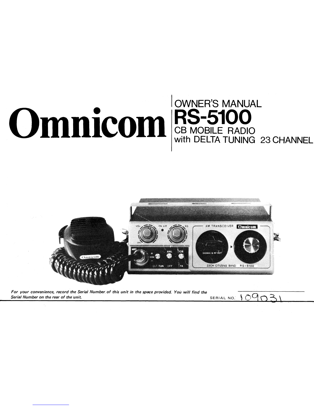
The Model RS-5100 is a fully transistorized transmitter-receiver capable of operating on any of 23 crystal-controlled
channels in 27MHz citizens radio band, and is designed to be used for either mobile or fixed station service.
It is developed through many years of our successful experiences in technology to provide sufficient transmitting power
and high receiving sensitivity; the advanced techniques employed in every part of the circuitry also assure marked
reliability and trouble-free performance.
The model comes complete with a variety of auxiliary devices such as built-in PA (public-address) amplifier, delta tune
switch, ANL (automatic noise limiter) switch, signal and RF power indicator, on-air lamp, jacks for external speaker
and PA speaker, etc., for added convenience of operation.
A microphone with press-to-talk button and a mounting bracket are also included. The model is powered by a 12V
negative or positive ground system car-battery or by an appropriate AC-DC converter for fixed station operation.
—1—

FCC DATA
PS-
MERITON ELECTRONIC, tr
SERIAL NO
BACK VIEW
-2-
FRONT VIEW
•

OPERATING PARTS
1.
MIC Connector
For connection of the supplied press-to-talk microphon e.
2.
Delta Tune Switch
Retunes the receiver in the input frequency when it cau ses drifting during reception.
3.
ANL Switch
Automatically reduces external electrical noise, such as pulse or ignition noise
introduced in receiving signals.
4.
CB/PA Switch
PA position is used only for public-address operation. For normal operation this
switch should be set to CB position.
5.
Squelch Control
Functions only in the receive mode. It silences the speaker while the signals are
absent and allows a quiet standby operation.
This control does not affect the receiver volume when signals are present.
6.
On-air Lamp
This lamp keeps lighting while the transmitter is in operation.
7.
OFF/Volume Control . . . . This control has two functions; power ON/OFF and receiver volume adjustments.
8.
Signal/Power Meter
A dual purpose meter which indicates relative output power during transmission and
input signal strength during reception.
9.
Channel Selector
Tunes the transmitter and receiver simultaneously in any of 23 channel frequencies.
10.
ANT Socket
For connection of antenna cable.
11.
EXT SP Jack
For connection of an external speaker.
This connection automatically shuts off the built-in speaker.
12.
PA SP Jack
For connection of a public-address speaker.
13.
Power Cable
This cable should be connected to a 12V car-battery or an AC-DC converter.
—3—

MOUNTING BRACKET
SPACER x 2
WASHER
x 2
-------- TAPPING SCREW x2
TOOTHED LOCK WASHER .2
WING BOLT x 2
INSTALLATION
A suitable place for installing the unit is under the dash of your car.
Installation is not complicated; it can be done by simply using the
supplied pre-drilled mounting bracket and complete set of screws and
nuts (see illustration for details). When choosing a mounting position,
be sure to observe the following precautions:
(1)
Avoid places in the vicinity of air conditioning or heating system
openings.
(2)
Installing place should be free from moisture and dust.
(3)
To ensure interference-free driving of car and for convenience of
operation, allow a proper spacing between the unit and the
driver's seat.
(4)
The unit should be installed where there is no direct transmittal
of vibrations. It should be either secured in position or held
with proper suspension springs.
ANTENNA CONNECTION
Antenna to be used should be of a type conforming to the FCC Regulations. Connect the antenna cable into the standard
"M" type ANT Socket provided on the rear of the unit. Proper antenna installation should be referred to the instruction
manual included with your antenna.
POWER CONNECTION
The power cable is color-coded to indicate polarity. Connect the red lead to the positive (+) post of a 12V car-battery
and the black lead to the negative () post. The unit permits connection to either negative or positive ground system
battery without requiring modifications.
Note: * Before making connection, ascertain that the OFF/Volume Control is in the extreme counterclockwise position
(power OFF).
* Be very careful not to connect the cable in wrong polarity. Wiring in wrong polarity will blow out the fuse (2A)
in the cable.

OPERATION
1.
PRELIMINARY PROCEDURE
Ascertain that the power and antenna cables are properly connected. Set the CB/PA Switch to the "CB" position
and the Squelch Control to the full counterclockwise position. Then proceed as follows:
(1)
Insert the microphone plug into the MIC Socket.
(2)
Rotate the OFF/Volume Control clockwise until a click is heard.
This turns the power on and illuminates the Signal/Power Meter.
(3)
Rotate the OFF/Volume Control further clockwise for suitable volume so that the rushing noise from the
speaker can be heard clearly.
(4)
Slowly rotate the Squelch Control clockwise until the noise from the speaker suddenly disappears and then
set the control there. This is the position at which optimum squelch effects can be obtained.
2.
TRANSMISSION & RECEPTION
CAUTION: DO NOT PUSH THE PRESS-TO-TALK BUTTON ON THE MICROPHONE WITHOUT CONNECTING
AN ANTENNA.
(1)
Set the switches and controls as follows:
Delta Tune Switch
Center position (NOM)
ANL Switch
ANL (ON) position
CB/PA switch
CB position
Squelch Control
As described under the item "Preliminary Procedure"
(2)
Connect the microphone and set the Channel Selector to the desired channel as indicated directly on the
selector knob.
(3)
Turn the power on and adjust the loudness of speaker.
(4)
To transmit push and hold the press-to-talk button on the microphone.
Hold the microphone about 5cm from your mouth and speak in a normal tone of voice.
—5—

(5)
When your transmission is completed, release the button on the microphone and you will hear your party's
voice. When receiving a weak station, rotate the Squelch Control slightly back for the strongest signal.
(6)
If the receiving frequency causes a drift when you are listening, retune the receiver by setting the Delta Tune
Switch to either "+" or "—" position, whichever tunes the receiver in the incoming frequency.
Note: * ANL OFF position is for operation in low noise area.
* If a larger audio output power is desired, connect an external speaker (8
ci)
to the EXT SP Jack.
PUBLIC
—
ADDRESS OPERATION
Your transceiver is provided with a built-in public-address amplifier so that it can be used as a public-address system.
Connect your existing PA speaker (8
ci)
to the PA SP Jack and set the CB/PA Switch to the PA position.
TECHNICAL PERFORMANCE
Dimensions and Weight:
26.965 — 27.255MHz, 23 channels
A3
600 ohms
12V negative or positive ground (Polarity Protector contained in unit)
Receive
approx. 200mA (squelch ON)
Transmit
approx. 1500mA (maximum mod.)
a.
Ambient temperature: —10
°
C — +50
°
C
b.
Relative humidity:
+40
°
C 95% or less
c.
Power Variation:
11V — 15V
a.
Dimensions:
165(W) X 55(H) X 200(D)mm
b.
Weight:
approx.1.5kg
GENERAL
Frequency Range:
Type of Emission:
Microphone:
Power Supply:
Power Consumption:
Operating Condition:

TRANSMITTER
Frequency Stability:
RF Output:
Modulation:
Harmonics and Spurious Emission:
Antenna Terminal Impedance:
RECEIVER
Sensitivity:
Selectivity:
Spurious Rejection:
AGC Characteristics:
Squelch:
AF Output:
Type of Speaker:
0.005% or better (-30
°
C — +50
°
C)
4 watts max.
95%
50dB or more below carrier level
50 ohms
0.50/ for 10dB S/N (30% mod.)
6dB at bandwidth 5.5kHz min., adjacent channel rejection 50dB min.
50dB min.
Within 10dB AF variation for 20/ — 1.0V RF input
Minimum sensitivity . . . 0.5V
Built-in speaker
1 watt
External speaker
3 watts
Dynamic type, 8 ohm
CHANNEL FREQUENCIES
(assigned by FCC)
Ch 1
26.965MHz
Ch 2
26.975
Ch 3
26.985
Ch 4
27.005
Ch 5
27.015
Ch 6
27.025
Ch 7
27.035
Ch 8
27.055
* emergency channel
* Ch
9
27.065MHz
Ch 10 27.075
Ch 11 27.085
Ch 12 27.105
Ch 13 27.115
Ch 14 27.125
Ch 15 27.135
Ch 16 27.155
Ch 17 27.165MHz
Ch 18 27.175
Ch 19 27.185
Cli 20 27.205
Ch 21
27.215
Ch 22
27.225
Ch 23
27.255
—7—

ADJUSTMENTS
ADJUSTMENT PROCEDURE
For adjustments of transceiver, connect a 50-ohm dummy load across the antenna terminals. It is recommended that
adjustment be made repeatedly according to the instructions given in the Adjustment Procedure Table.
1.
Pull out the chassis toward the front panel (remove screws on casing).
2.
Maximum modulation degree is 90%. Level setting for over-modulation protection should be performed by VR5.
3.
Standard modulated input (50% mod.) for the microphone is 2mV/600 ohms at lkHz.
4.
Squelch adjustment: Turn the squelch knob fully clockwise. Connect SSG to the antenna terminals and feed
40dB input. Adjust VR3 until squelch opens. Then remove the input signal and turn the squelch knob fully
counterclockwise whereby noise will be heard from the speaker. Turn the knob slowly in clockwise direction and
squelch will be on at approximately 1/3 position of the turning range. Set the knob there. Feed 0dB input signal
from SSG and check that squelch is working properly.
5.
Meter setting:
a)
RF output
Adjust VR6 so that meter reading shows the 2/3 position on the meter scale while transmitting through 50-ohm
dummy load.
b)
Input signal
With 90dB signal fed from SSG, adjust VR1 until the meter reading shows the full right position "10" of the
meter scale in the receive mode.
Note: Power consumption under normal operation:
Receive (squelch on)
200mA (approx)
Transmit (no mod.)
800mA (approx)
Transmit (full mod.)
1300mA(approx)
—8—

ADJUSTMENT PROCEDURE TABLE (transmitter)
Item
Adjusting
Point
Test
Point
Procedure
Test
•
Instrument
1
Oscillator
L109
TP-3
Set channel to Ch.23. Align L109 until Freq.
Freq. counter
(37MHz)
Counter shows 37.850MHz when VTVM is in
full scale.
RF VTVM
Fix L109.
Standard voltage at TP-3 is 0.8 — 0.9V.
2
Mixer
L110
TP-5
Set channel to Ch.9. Align L110, L111 until
RF VTVM
L111
VTVM on TP-5 shows full scale reading.
Standard voltage at TP-5 is 0.35V.
3
Exciter
L112
TP-7
Set channel to Ch.9.
Align L112 and L113
DC ammeter
(Buffer
driver)
L113
for maximum current on DC ammeter con.
nected to TP-7.
Standard current at TP-7 is 0.4mA.
4
Power
L116
Ant.
Align L116 and L117 for maximum power,
50-ohm
amp.
L117
terminal
with dummy load connected to antenna
terminals.
Then align L112 and L113 for
maximum power.
dummy load
Standard output is 3 — 3.2W.

Item
Adjusting
Point
Test
Point
Procedure
Test
Instrument
5
Modulation
R46
Ant.
terminal
Feed 2.5kHz AF oscillator output to micro-
phone.
Adjust AF input level until 50%
modulation
wave
is
seen on oscilloscope.
Increase AF input level 16db (6 times) at 50%
modulation.
Adjust VR5 and fix it where
modulation degree does not exceed 90%.
Standard AF input level at 50% modulation is
approx. 2mV/600 ohms.
AF oscillator
Oscilloscope
AF VTVM
Note:
1.
All adjustments should be made under channel 9, except 37MHz oscillator adjustment.
2.
All test points are "plus" polarity except TP-7.
3.
Polarity of TP-7 is "minus" at choke coil L114 and "plus" at power source.
4.
TP-8 is "minus"

ADJUSTMENT PROCEDURE TABLE (receiver)
Item
Adjusting
Point
Test
Point
Procedure
Test
Instrument
1
AF
Amplifier
None
Speaker
terminal
(EXT SP
JACK)
With 10mV signal applied to both inputs' of
VR2,
check wave
and output voltage at
speaker terminals.
The
output voltage is
approx. 3V.
No remarkable distorted wave
should be observed.
Speaker impedance is
8 ohms.
AF oscillator
VTVM
Oscilloscope
2
2nd IF
L106
L107
L108
EXT SP
JACK
Accurately align SSG freq. to 455kHz and
feed 20db output power (30% mod) from
TP-2.
Align L106 thru L108 for maximum
AF output.
The circuits after 2nd IF are
normal, if AF output at EXT SP JACK reads
3V/8-ohm when the input is lowered to 15db.
SSG
VTVM
Oscilloscope
3
2nd local
oscillator
(10MHz)
None
TP-4
Set channel to Ch.9.
Connect Freq. Counter
and VTVM to TP-4.
Accurate 10.180MHz on Freq. Counter.
Standard voltage at TP-3 is 0.4 '
0.6V.
Freq. counter
VTVM

Item
Adjusting
Point
Test
Point
Procedure
Test
Instrument
4
1st IF
L104
EXT SP
Set channel to
Ch.11.
Adjust SSG freq.
SSG
L105
JACK
sharply for 10.615MHz.
With about 20db
output (30% mod) applied to TP-1, adjust
VTVM
Oscilloscope
L104 and L105 until maximum output is
obtained at EXT SP JACK.
The measured AF output should be about
3V/8-ohm, with 10db input applied to TP-1.
5
1st local
oscillator
(37MHz)
L109
TP-3
This stage is used in common with the oscilla-
tor on transmitter section.
For alignment,
refer to the instructions given in transmitter
section.
Freq. counter
VTVM
6
RF
L101
EXT SP
Set channel to Ch.9 and SSG freq. to the Ch.9
SSG
amplifier
L102
JACK
frequency.
With 10db output (30% mod)
VTVM
L103
applied to antenna terminal, adjust L101-
Oscilloscope
'
L103 for maximum output at EXT SP JACK,
which should be about 3V/8-ohm at 2-3db of
RF input.
Note: 1. When checking AF output, EXT SP JACK should be terminated with an 8-ohm speaker or a
noninductive resistor.
2.
SSG connection to TP-1 or TP-2 must be made thru 0.04 —0.11/F capacitor.
—1
2—

" T
.(
0I
L'SC
JSP-7001
ADJ 0-18P
M
K
3
C39
33.37K ebur T ACH)
1NTS
5
6
ce1;
5
4TiL
281(SC)
sIALTEV'ER
F
47K YSOKB
ra
.832
2V1 2
OHO
{8,7
Art
g8
7
7
P$
p
6K
(
i;
330
R~6 C75
lob
R
470
7121
?as-
2
C95 C
`
(0
.
P
58
22
Tl°
56
ic
l l3
Q8
SQUELCH
JA-I350
"2473vE
IO
13R
nr<
7.P
QI
RF AMP
Q2 1st
MIXER
Q3 2nd
MIXER
Q4
IF AMP
Q5
IF AMP
JSP
-
700I
JSP-700I
JSP-700I
JA-1350
JA
-
1350
C.82
R6 560
2
IOOP
Z.
)
BAAO
D3
OB
C
a2
LIOI
91.(CH)
VR2 C34
"
022
°
1,
1
s,3
560
S
=
LC H
EXT S.P JACK
QI1:
i
AF
AMP
J
51
(SC)
A
D I
R62
CB P
R 2
0
MIC
R
gg
MIC ASSY
$i SK
R 7
IND LAMP
DIB
°PA-
.
T
X
9,13-70'.1x
3P
(CH
020 airier
Arad
JA- 7001
Q22
FIN, AMP
MPSU- 31
C92 2P (CH)
Ferrite Bead
—13—
C109 0100 C101 CI02 C103
ciO4 c.
F
ci°22
PA SP JACK
OMN leoN1 RS-5100
SCHEMATIC DIAGRAM

EXTERNAL SP. JACK
PA.SP.JACK
it
L117
D15
017
VR5
DI9*
DI
DI3
*
4 t
V
p
R
:
= Q22
TPI
•
0
02
TP6
.
IQ
21
LII2
L101
L103
LI04
LII6
LII5
T 3
DI4
DI7
T I
012
1 1
DII
T2
013
014
0
*D7
DIO
D5
*D.
ANTENNA CONNECTOR
PARTS LOCATION
ION
D.0 POWER SUPPLY
U
016
0
(
its
02
4'-
O
Q15
q
.
QI
L102
.TP2
LI05
03
LIII
LII0
TP3
06
0Q7
,--220 •
Ci
C)
0-
„
L109
TP4
. CH3 CHI
ZP5D14° ()(E)1
Dt
88000
0Q19 0018 (
)
(
X10
)
R3
L106
C.,
L107
Q5
f"
--
N
X6
1)3
L1013
*VRI
D20 D4
(014
SQUELCH
VOLUME CONTROL WITH POWER
SW
CB. PA. FUNCTION SW
ANL. SW
DELTA TUN
MIC . CONNECTOR
-14-
CHANNEL SELECTOR

PARTS LIST
Symbol
No.
Code No.
Description
Symbol
No.
Code No.
Description
Q
1
16304197001
JSP-7001
RF Amp
D
1
16411992473
IS-2473
Diode
2
16304197001
JSP-7001
1st Mix
2
16411992473
IS-2473
Diode
3
16304197001
JSP-7001
2nd Mix
3
16411190188
IS-188AM
Diode
4
16304191350
JA-1350
IF Amp
4
16411190188
IS-188AM
Diode
5
16304191350
JA-1350
IF Amp
5
16411190188
IS-188AM
Diode
6
16304197001
JSP-7001
1st Local OSC
6
16411190188
IS-188AM
Diode
7
16304197001
JSP-7001
2nd Local OSC
7
16461992473
IS-2473VE
Diode
8
16304191350
JA-1350
Squelch
9
16304191350
JA-1350
Squelch
9
16461992473
IS-2473VE
Diode
10
16304191350
JA-1350
AF Amp
10
16461992473
IS-2473VE
Diode
11
16304191600
JA-1600
AF Drive Amp
11
16515991002
SRIK2
Diode
12
16304199400
MJE-9400
AF Final Amp
12
16411190188
IS-188AM
Diode
13
16304199400
MJE-9400
AF Final Amp
13
16411190188
IS-188AM
Diode
14
16304191350
JA-1350
MOD Amp
14
16515991002
SR1K2
Diode
15
16304191350
JA-1350
MOD Cont.
15
16602995856
1N-5856
Zener
16
16304191350
JA-1350
Switch
16
16602990107
EQA01-07
Zener
17
16004191050
JA-1050
Switch
17
16515991002
SR1K2
Diode
18
16304191350
JA-1350
TX OSC
18
16602995856
1N-5856
Zener
19
16304197001
JSP-7001
TX Mix
19
16411190188
IS-188AM
Diode
20
16304197001
JSP-7001
Suffer Amp
20
16411190188
IS-188AM
Diode
21
16304198000
MPS-8000
Drive Amp
LED
16669990103
SEL-103R
TX IND
22
16304190031
MPSU-31
Final Amp
—15—

Symbol
Code No.
No.
Description
Description
Symbol
No.
Code
No.
X
1
06300077870
37.600MHz
Crystal
L 110
00009077889
27MHz
TX RF Coil
2
06300077871
37.650
-
Crystal
111
00009077889
27MHz
TX RF Coil
3
06300077872
37.700
-
Crystal
112
00009077889
27MHz
TX RF Coil
4
06300077873
37.750
-
Crystal
113
00009077890
27MHz
TX RF Coil
5
06300077874
37.800
-
Crystal
114
00019077891
27MHz
RF Choke
6
06300077875
37.850
-
Crystal
115
00079077892
27MHz
TX RF Coil
7
06300077876
10.635
-
Crystal
116
00079077893
27MHz
TX RF Coil
8
06300077877
10.625
-
Crystal
117
00056077894
27MHz
TX RF Coil
9
06300077878
10.615
-
Crystal
10
06300077879
10.595
-
Crystal
CH 1
00022077896
RF Choke Coil
11
06300077880
10.180
-
Crystal
3
00027086343
Choke Coil
12
06300077881
10.170
-
Crystal
13
06300077882
10.160
-
Crystal
14
16300077883
10.140
-
Crystal
CF
06312077897
CFU-455H
Ceramic Filter
L101
00009077884
27MHz
RX RF Coil
455kHz
102
00009077885
27MHz
RX RF Coil
103
00009077885
27MHz
RX RF Coil
T
1
10429877900
Choke Trans
104
00100077886
10.615MHz
1st IFT
2
10203877898
Input Trans
105
00100077886
10.615MHz
1st IFT
3
10376877899
Output Trans
106
00700077887
455kHz
2nd IFT
107
00701078170
455kHz
2nd IFT
VR 1
01736487800
Semi-fixed VR
108
00702078171
455k1-rz
2nd IFT
2
01196061055
Volume Cont.
109
00009077888
38MHz
OSC Coil
3
01736487800
Semi-fixed VR
—16—

Symbol
No.
Code No.
Description
Symbol
No.
Code No.
Description
VR 4
5
SWa-C
SP, PA
PA, SP
MIC
SP
01196061056
01736487800
04192561060
04892061218
04892061219
04894061220
05010082809
05010082809
13219061057
05610076997
03170061058
15124088858
05620078115
07091061059
14002071738
14099078116
15000078180
Volume Cont.
Semi-fixed VR
CH
Rotary Switch
PA/CB
Lever Switch
ANL
Lever Switch
DLT TUN Lever Switch
External SP Jack
PASP out Jack
600 ohms
Microphone
M type
Antenna connector
8 ohms
Speaker
2A
Fuse
Fuse Holder
400µA
Meter
6V/30mA Lamp
6V/80mA Lamp
PC Board
R
1
2
3
4
5
6
7
8
9
10
11
12
13
14
15
16
17
18
19
20
21
22
(All resistance
solid type unless
11054696801
11054693300
11054695600
11054696801
11054691001
11054695600
11054695600
11054696801
11054691001
11054695600
11054691001
11144691003
11054692201
11054691003
11054691002
11054691001
11054695602
11054695600
11054691801
11054691002
11054693300
11054692200
values are in E2, ±10%,'4W, and
otherwise indicated.)
6.8k
330
560
6.8k
.
1k
560
560
6.8k
1k
560
1k
100k
Carbon
2.2k
100k
10k
1k
56k
560
1.8k
10k
330
220
—17—

Symbol
No.
Code No.
Description
Symbol
No.
Code No.
Description
R 23
11144692202
22k
Carbon
R
47
11044693301
3.3k
24
11054695602
56k
48
11044692202
22k
25
11054691003
100k
49
11054695601
5.6k
26
11054696802
68k
50
11044691502
15k
27
11054696802
68k
51
11054691000
100
28
11144691004
1M
Carbon
52
11044692200
220
29
11054691001
1k
53
11044691000
100
30
11054693301
3.3k
54
11044691001
1k
31
11054691502
15k
55
11816690005
0.5
1W
Metal Film
32
11054693300
330
56
11054691501
1_5k
33
11044690560
56
57
11054693301
3.3k
34
11054691001
1k
58
11054691001
1k
35
11816690080
8 1W
Metal Film
59
11144692202
22k
Carbon
36
11054691001
1k
60
11144698201
8.2k
Carbon
37
11054693301
3.3k
61
11054691000
100
38
11054696801
6.8k
62
11054692200
220
39
11054695600
560
63
11054692200
220
40
11044690560
56 64
11054692200
220
41
11054691502
15k
65
11054695601
5.6k
42
11054691003
100k
66
11054691501
1.5k
43
11054691501
1.5k
67
11054690560
56
44
11144693302
33k
Carbon
68
11045690750
75
ww
45
11144694701
4.7k
Carbon
69
11045691500
150
1
/
2
W
46
11054691001
1k
70
11045691500
150
1
/
2
W
—18—

Symbol
No.
Code No.
Description
Symbol
No.
Code No.
Description
R
71
72
73
74
75
76
77
78
79
80
81
82
83
84
85
86
87
88
89
90
91
92
93
11054695601
11054693300
11054691502
11044690560
11054691502
11054692201
11054691000
11054691002
11054691001
11054690220
11054690560
11054691000
11054690056
11054691500
11054690220
11054694700
11054694701
11054695601
11054695601
11054693301
11054691002
11044696801
11054695602
5.6k
330
15k
56
15k
2.2k
100
10k
1k
22
56
100
5.6
150
22
470
4.7k
5.6k
5.6k
3.3k
10k
6.8k
56k
C
1
2
3
4
5
6
8
9
10
11
12
13
14
15
16
17
18
19
20
21
22
23
(All capacitance values
ceramic type unless
12530490390
12501692002
12530490120
12501692002
12530490680
12530090040
12530490680
12501692002
12501692002
12501692002
12530490220
12520191002
12501692002
12530090030
12501692002
12520194702
12530490150
12501692002
12313091005
12501692002
12520194702
12501692002
are in ALF,
-
4%, 50V and
otherwise indicated.)
39P (CH)
±10%
0.022
12P (CH)
±10%
0.022
68P(CH)
±
-
10%
4P (CH)
±
-
0.5P
68P(CH)
-
±10%
0.022
0.022
0.022
22P (CH)
±10%
0.01
25V
0.022
3P (CH)
±0.5P
0.022
0.047
25V
15P (CH)
±10%
0.022
10
4
°
70 16V Elec.
0.022
0.047
25V
0.022
—19—
Table of contents