OTRONA ATTACHE User manual

Attache
.
Portable
Computer
Technical
Manual
.Hardware
Theory
of
Operation
Software
Appendixes
OTRONA
Attache
Portable
ca.puter
Technical
Manual
Published
by
Otrona
Advanced Systems
Corporation
Copyright
1983 by
Otrona
Advanced Systems
Corporation
Otrona Pub.
No.
92051210
Version
1.1
July,
1983

CcmYright
Copyright
(c)
1982
by
Otrona
Corporation.
All
rights
reserved~
No
part
of
this
publication
may
be reproduced,
transmitted,
transcribed,
stored
in
a
retrieval
system,
or
translated
into
aQY
language
or
computer
language,
in
any
form
or
by any means,
electronic,
mechanical,
magnetic,
optical,
chemical,
manual,
or
otherwise,
without
the
prior
written
permission
of
Otrona
Corporation,
4755
Walnut
st.,
Boulder,
Colorado
80301.
Disclaimer
Otrona
Corporation
makes no
representations
or
warranties
with
respect
to
the
contents
hereof
and
especially
disclaims
any
implied
warranties
of
merchantability
or
fitness
for
any
particular
purpose.
Further,
Otrona
Corporation
reserves
the
right
to
revise
this
publication
and
to
make
changes
f rom
time
to
time
in
the
content
without
obliga
tion
of
Otrona
Corporation
to
notify
any
person
of
such
revisions
or
changes.
Trademarks
ATTACHE,
Charton,
and
Valet
are
trademarks
of
Otrona
Corporation,
4755
Walnut
st.,
Boulder,
Colorado.
References
are
made
throughout
this
document
to
the
WordStar
word
processing
system
and
to
the
Control
Program
for
Microcompute~s,
commonly
Known
as
CP/M.
WordStar
is
a
registered
trademark
of
MicroPro
International
Corporation
of
San
Rafael,
California.
CP/M
is
a
trademark
of
Digital
Research
Inc.
of
Pacific
Grove,
California.

PREFACE
Bow
to
Use
This
Manual
This
manual
is
intended
for
readers
with
knowledge
of
electronics
or
software
who
seek
information
about
Attache's
design
or
interface
capabilities.
The
manual
is
divided
into
three
sections.
The
first
section
is
an
overview
of
Attache
hardware,
which
contains
a
general
description
of
the
five
Attache
modules:
the
processor
board,
the
display,
the
diskette
drives,
the
keyboard, and
the
power
supply.
The
second
section
is
the
theory
of
operations,
which
contains
a
description
of
system
logic
flow and
the
theory
of
operations
for
each
of
the
seven
logic
sections
on
the
processor
board.
The
logic
sections
are
clearly
marked
on
the
board
with
white
borders.
Each
section
corresponds
to
a
schematic
page
in
Appendix
A.
The
logic
of
the
modules
is
also
described.
The
third
section
of
the
manual
concerns
Attache
software.
This
chapter
describes
BIOS
(Basic
Input/Output
System),
ROM
(Read-Only
Memory)
software,
and
memory
locations.
Common
programming
functions
are
included
with
the
appropriate
software
topic,
and
are
also
listed
as
illustrati.ons
on
page
viii
for
quick
referencing.
Appendix A
contains
Attache
schematics.
Appendix B
is
a
list'
of
referenced
publications.
Appendix C
is
a
list
of
acronymns.
Appendix D
is
the
glossary.
Appendix E
is
the
index.
i

Contents
I.
Hardware
Hardware Overview ......................................
Attache
System .........................................
........................................
Processor
Board
Processor
Memory
..................................
..........................................
·..........................................
I/O
RTC
Floppy Disk .......................................
"",.:
,.,..
.......
,
.......
.LI.J.O
,t'..LQ.,y ·..........................' ................
..........................................
Graphics
Serial
............................................
Expansion
O~ion
..................................
Display
~
...............................................
Alphanumeric
Display
..............................
Graphic
Display
·..................................
Diskette
Drives
••••••••••••••••••••••••••••••••••••••••
Standard
Format ·
..................................
.
Keyboard ...............................................
Multi-function
Keys .......................... .
..
la-Key
Mode
.......................................
Power
Supply
•••••••••••••••••••••••••••••••••••••••••••
Setting
the
Voltage
............................
II.
'l'beory
of
Operations
ii
Introduction
·..........................................
System Block Diagram ·...................................
Logic
Overview .........................................
Processor
..............................................
Central
Processing
unit
...........................
Pin
Functions
·....................................
Direct
Memory
Access
Controller
.................
Pin
Functions
·.................................
DMA
Operation
·
....................................
.
·
....................................
.
I/O
Selection
Expansion
Connector
...............................
1-1
1-2
1-3
1-3
1-4
1-4
1-4
, A
J.-~
1-4
1-5
1-5
1-5
1-5
1-6
1-6
1-6
1-7
1-7
1-7
1-8
1-8
2-1
2-2
2-4
2-6
2-7
2-7
2-8
2-8
2-9
2-10
2-10
Memory
•••••••••••••••••••••••••••••••••••••••••••••••••
Addressing
RAM
•••••••••••••••••••••••••••••••••••
Writing
or
Reading
Data
•••••••••••••••••••••••••••
Generating
RAS/CAS
••••••••••••••••••••••••••••••••
Memory
Mapping
••••••••••••••••••••••••••••••••••••
Erasable
Programmable Read-Only
Memory
••••••••••••
.................................................
Serial
Clock
Reset
.............................................
.............................................
Serial
Input/Output
Controller
••••••••••••••••••••
Pin
Functions
••••
~
••••••••••••••••••••••••••••••••
SIO
Operation
·....................................
.......................................
The
Ports
Jumpers ..........................................
Counter Timer
Circuit
·............................
·....................................
Pin
Functions
Interrupts
·.......................................
Display
................................................
I/O
................
-..................
Cathode
Ray
Tube
CRT
Controller
Pin
Functions
....................................
·....................................
Timing ............................................
Reading
or
Writing
to
the
Screen
••••••••••••••••••
Selecting
the
Address !
·............................
Writing
the
Data
on
the
Screen
•••••••••••••••••••••
Attributes
Graphics
·.......................................
..........................................
RTC
.................................................
Parallel
Input/Output
Controller
••••••••••••••••••
Pin
Functions
·....................................
Sound
Effects
Generator
...........................
CMOS
Random
Access
Memory
•••••••••••••••••••••••••
Control
Latch
·....................................
·..................................
Real
Time
Clock
Keyboard
Interface
................................
Floppy
..................................................
Basic
Mechanism ·..................................
Read/Write
·.......................................
Writing
Data on
the
Diskette
••••••••••••••••••••••
MFM
and
FM
·.......................... .
.........
.
Reading Data
From
the
Diskette
••••••••••••••••••••
·..................................
Diskette
F'ormat
Diskette
Track
Format ·............................
2-11
2-12
2-14
2-15
2-16
2-17
2-18
2-19
2-19
2-20
2-20
2-21
2-21
2-23
2-26
2-26
2-27
2-29
2-31
2-32
2-32
2-33
2-36
2-36
2-38
2-39
2-40
2-42
2-43
2-43
2-44
2-44
2-45
2-45
2-46
2-47
2-48
2-49
2-49
2-50
2-52
2-54
2-55
Graphics
••••••••••••
_
•••••••••••••••••••••••••••••••••••
2-56
iii

Power .Supply
•••••••••••••••••••••••••••••••••••••••••••
Introduction
••••••••••••••••••••••••••••••••••••••
AC
Power Module ·..................................
...........................
Control
Power
Regulator
Pulse
Width
Modulator
.............................
PWM
Dead Time .....................................
Over-current
and
Soft
start
•••••••••••••••••••••••
High
Voltage
Driver
Board
•••••••••••••••••••••••••
Flyback
Transformer
...............................
Output
Supply
Rectifiers
and
Filters
••••••••••••••
.................................
Power Okay
Sensor
Voltage
Monitor
·..................................
Fan
Driver
Connectors
·........................................
·.......................................
Keyboard ............................................
Introduction
•••••••••••
........................
..............................
Basic
Keyboard
Logic
Additional
Circuitry
FunctionS
....................
Keyboard
Layout
·...................................
ASCII
Character
Codes .............................
.........................................
·.......................................
Display
Module
Horizontal
Vertical
Video
..........................................
.............................................
CRT
...............................................
Diskette
Drive
•••••••••••••••••••••••••••••••••••••••••
Head Movement ............................
.....
Sensors
Writing
Reading
Turning
·...........................................
·............................; ..............
·..........................................
the
Diskette
..............................
2-57
2-58
2-58
2-60
2-60
2-61
2-62
2-63
2-64
2-64
2-65
2-66
2-66
2-66
2-67
2-68
2-69
2-70
2-70
2-71
2-72
2-73
2-74
2-74
2-75
2-76
2-78
2-78
2-79
2-81
2-82
III.Software
Software
Introduction
..................................
3-1
CP/M
Introduction
••••••••••••••••••••••••••••••••••••••
3-2
CP/M
Memory
Locations
...................................
3-3
Low
Memory
Map
•••••••••••••••••••••••••••••••••••••••••
3-4
IOBYTE
.................................................
3-6
iv

ROM
Software
••••••••••••••••••••••••••••••••••••••••••••
Terminal
Emulation
••••••••••••••••••••••••••••••••
Monitor
Mode
-
Diagnostics
••••••••••••••••••••••••
Generate
Display
Pattern
••••••••••••••••••••••••••
Display
RAM
Test
••••••••••••••••••••••••••••••••••
Input
Test
••••••••••••••••••••••••••••••••••••••••
Jump
••••••••••••••••••••••••••••••••••••••••••••••
.....................................
........................................
Keyboard
Test
Loop
Tests
Map
Test
Output
Test
..........................................
.......................................
Format
Diskette
Test
·.............................
CMOS
RAM
Test
•••••••••••••••••••••••••••••••••••••
Main
RAM
Test
.....................................
Select
Output
Ports
Real-Time Clock
Test
·..............................
·.............................
United
Tests
••••••••••••••••••••••••••••••••••••••
Read a
Sector
From
a Disk
Write
a
Sector
to
a Disk .........................
..........................
.................................
I/O
Port
Transmit
I/O
Port
Receive
Automatic Disk
Test
..................................
·..............................
BIOS
Introduction
.......................................
Boot Loader
Cboot
............................................
.............................................
Disk
............................................
Driver
Blocking/Deblocking
Physical
Read/Write ·..............................
·
.............................
.
Input/Output
Driver
••••••••••••••••••••••••••••••••••••
Additional
Functions
·.............................
Z80
SIO
Initialization
••••••••••••••••••••••••••••
Progranuning
the
SIO
Baud Rate
•••••
'
••••••••••••••••
I/O
Ports
.........................................
Display
Driver
.........................................
Accessing
the
Display
Driver
••••••••••••••••••••••
Character
Transmission
••••••••••••••••••••••••••••
Attribute
Transmission
••••••••••••••••••••••••••••
Display
Control
Parameters
Transmission
•••••••••••
Graphic
Data
Transmission
•••••••••••••••••••••••••
Attache
Escape
Commands
................................
Graphic
Escape
Commands
•••••••••••••••••••••••••••
Cursor
Control
Escape
Commands
••••••••••••••••••••
Clear
and
Delete
Escape
Commands
••••••••••••••••••
Insertion
Escape
Commands
•••••••••••••••••••••••••
Screen
Parameter Escape
Commands
••••••••••••••••••
System
Control
Escape
Commands
••••••••••••••••••••
Attache
Control
Character
Codes
.........................
3-7
3-8
3-10
3-11
3-11
3-11
3-12
3-12
3-12
3-13
3-13
3-13
3-14
3-14
3-15
3-15
3-16
3-16
3-17
3-17
3-17
3-18
3-19
3-20
3-20
3-21
3-21
3-21
3-24
3-24
3-25
3-26
3-28
3-30
3-31
3-31
3-32
3-32
3-33
3-34
3-34
3-35
3-35
3-36
3-36
3-38
3-39
v
Screen
Attribute
Codes ·................................
·................................
Attache
Character
Sets
Character
Size
Selection
..........................
CMOS
RAM,
Clock,
and
Sound
Generator
•••••••••••••••••••
CMOS
Memory
Allocation
............................
Programming Sounds
or
Alanns
••••••••••••••••••••••
Attache
Clock .....................................
·....................................
Interrupt
Structure
Introduction
......................................
I/O
Device
Interrupts
.............................
Floppy
Interrupts
••
~
•••••••••••••••••••••••
60
Hz
Interrupts
••••••••••••
:::::
••••••••••
.......
Generation
of
Keyboard
Character
Code
••••••••••••••••••
Physical
Keyboard
Layout
••••••••••••••••••••••••••
ASCII
Translation
·................................
Determining
the
Character
Code
••••••••••••••••••••
Character
Codes
as
Stored
in
BIOS
•••••••••••••••••
Changing a Keycode
in
Memory
••••••••••••••••••••••
Valet
..................................................
Hexadecimal
Conversion
Chart
...........................
APPENDIXES
A.
Schematics
·..........................................
.........................................
Processor
Memory
·
..........................................
.
Serial
·............................................
Display
•••••••••••••••••••••••••••••••••••••••••••
...........................................
I/O
RTC
Floppy
Graphics
Power Supply
·...........................................
·.........................................
......................................
·.........................................
Keyboard
Display
Module ·...................................
Diskette
Drives
A
••
-
•••••••••••••••••••••••••••••••
Diskette
Drives
B ·................................
B.
Referenced
Publications
.............................
c.
List
of
Acronyms ·...................................
3-40
3-42
3-43
3-44
3-44
3-45
3-47
3-48
3-48
3-49
3-51
3-53
3-53
3-53
3-55
3-57
3-58
3-59
3-59
A-I
A-I
A-2
A-3
A-4
A-5
A-6
A-7
A-8
A-9
A-IO
A-II
A-12
B--I
C-l
D.
Glossary
••••••••••••••••••••••••••••••••••••••••••••
D-l
E.
Index
...............................................
E--J.
vi

LiQt
~
Illustrations
Hardware
1-1
1-2
2-1
2-2
2-3
2-4
2-5
2-6
2-7
2-8
2-9
2-10
2-11
2-12
At
tache
System
•••.••••••••••••••••••.••••••••••••••••••••
Processor
Board
•••••••••••••••••••••••••
~
••••••••••••••
System Block Diagram
•••••••••••••••••••••••••••••••••••
Processor
Block Diagram
••••••••••••••••••••••••••••••••
DMA
Timing
••••••••••••••••.•••••.••••••••••••••••••
'
••••••
Memory
Block Diagram
•••••••••••••••••••••••••••••••••••
Addressing
Memory
••••••••••••••••••••••••••••••••••••••
Reading
Data
from
Memory
•••••••••••••••••••••••••••••••
RAS/CAS
Schematic
••••••••••••••••••••••••••••••••••••••
Memory
Mapping
•••••••••••••••••••••••••••••••••••••••••
Serial
Block Diagram
•••••••••••••••••••••••••••••••••••
Jumt:er
Options
•••••••••••••••••••••••••••••••••••••••••
Daisy
Chained
Interrupts
..............................
..
Display
Block Diagram
••••••••••••••••••••••••••••••••••
2-13
CRT
Screen
•••••••••••••••••••••••••••••••••••••••••••••
2-14
2-15
2-16 ........................................
Video
Character
Display
Timing
Addressing
the
Display
·........................................
.................................
2-17
Graphic
Pixels
·........................................
2-18
Input/Output
-Real Time Clock Block Diagram
•••••••••••
2-19 Floppy Block Diagram
•••••••••••••••••••••••••••••••••••
2-20
Write
Precomt:ensation
••••••••••••••••••••••••••••••••••
2-21 Clock and
Data
Timing ..................................
2-22
Data
Separator
2-23
Diskette
Format·
........................................
.
........................................
2-24
Diskette
Track
Format .................'
................
.
2-25
2-26
2-27
2-28
2-29
2-30
2-31
Graphics
Block Diagram
•••••••••••••••••••••••••••••••••
Power Supply Block Diagram
•••••••••••••••••••••••••••••
Power Cords
••••••••••••••••••••••••••••••••••••••••••••
Keyboard Block Diagram
•••••••••••••••••••••••••••••••••
Keyboard
Grid
•••••••••••••••
~
••••••••••••••••••••••••••
Keyboard Layout ••
.-
•••••••••••••••••••••••••••••••••••••
ASCII
Chart
••••••••••••••••••••••••••••••••••••••••••••
2-32
Display
Module Block Diagram
•••••••••••••••••••••••••••
2-33a
Drive
Handle ..........................................
2-33b
Drive
Handle
••••••••••••••••••••••••••••••••••••••••••
2-34
Diskette
Drive
Block Diagram
•••••••••••••••••••••••••••
2-35
Write
Timing ...........................................
2-
36
Head
Diagr
am
•••••••••••••••••••••••••••••••••••••••••••
2-
37
Read
Signals
•••••••••••••••••••••••••••••••••••••••••••
2-
38 Se
rvo
System
•••••••••••••••••••••••••••••••••••••••••••
Page
1-2
1-3
2-2
2-6
2-9
2-11
2-13
2-14
2-15
2-16
2-18
2-22
2-28'
2-30
2-31
2-33
2-35
2-36
2-41
2-42
2-47
2-49
2-51
2-52
2-54
2-55
2-56
2-57
2-58
2-67
2-68
2-70
2-71
2-72
2-76
2-76
2-77
2-79
2-80
'2-81
2-82
vii

Liat
~
Illustrations
Software
3-1
3-2
3-3
3-4
CP/M
Memory
Map
•••••••••••••
~
••••••••••••••••••••••••••
Low
Memory
Maps
••••••••••••••••••••••••••••••••••••••••
File
Control
Block .....................................
IOBYTE
..................................................
3-5
ADM-3A
Control
Codes
•••••••••••••••••••••••••••••••••••
3-6
DEC
VT52
Escape Codes
••••••••••••••••••••••••••••••••••
3-7
Changing Baud
Rates
in
Terminal
Emulation
••••••••••••••
3-8
Monitor
Mode
Diagnostics
•••••••••••••••••••••••••••••••
3-9
Disk
Read
Operation
••••••••••••••••••••••••••••••••
,
••••
3-10
Programming
I/O
Devices
••••••••••••••••••••••••••••••••
3-11
Programming Baud
Rates
•••••••••••••••••••••••••••••••••
3-12
Writing
to
the
CTC
•••••••••••••••••••••••••••••••••••••
3-13
I/O
Ports
..
'
...........................................
.
3-14
3-15
3-16
3-17
Writing
to
the
Display
•••••••••
'
••••••••••••••••••••••••
Display
Control
Escape
Commands
••••••••••••••••••••••••
System
Control
Escape
Commands
•••••••••••••••••••••••••
Control
Character
Codes
................................
3-18
Coding
Screen
Attributes
•••••••••••••••••••••••••••••••
3-19
3-20
Character
Sets
•••••••••••••••••••••••••••••••••••••••••
CMOS
Allocation
Table
••••••••••••••••••••••••••••••••••
3-21
Baud
Rates
•••••••••••••••••••••••••••••••••••••••••••••
3-22
3-23
3-24,
3-25
3-26
3-27
3-28
viii
Key
Sounds
•••••••••••••••••••••••••••••••••••••••••••••
Progr
amming
Alarms
•••••••••••••••••••••••••••••••••••••
Accessing
the
Clock
••••••••••••••••••••••••••••••••••••
Programming
Interrupt
Driven
I/O
•••••••••••••••••••••••
Generating
Keyboard
Character
Codes
••••••••••••••••••••
Keyboard
Character
Codes
in
BIOS
•••••••••••••••••••••••
Hexadecimal
Conversion
Chart
•••••••••••••••••••••••••••
Page
3-3
3-4
3-5
3-6
3-8
3-8
3-9
3-10
3-23
3-25
3-26
3-27
3-29
3-33
3-34
3-38
3-39
3-40
3-42
3-44
3-45
3-45
3-46
3-47
3-50
3-53
3-57
3-58
CONTENTS
Overvie\v
...............
1
The
Attache System . . . . .
..
2
Processor Board. . . . . . . .
..
3
Display
.................
5
Disk Drives . . . . . . . . . . . .
..
6
Keyboard
...............
7
Power
Supply . . . . . . . . .
....
8
Hardware
Hard\vare
Hardware
Hardware Oyerview
This
section
is
an
overview
of
Attache
system
hardware.
Attache
is
divided
into
five
basic
modules:
the
processor
board,
the
display,
the
diskette
drives,
the
keyboard, and
the
"power
supply.
Processor
Board
Contains
the
system
control
and
interface
logic.
Display
Screen
5.5"
diagonal
CRT
with
24
lines
of
80
characters
(or
24
lines
of
40
double-size
characters)
and
320 x 240
dot
array
for
graphics.
Diskette
Drives
Two
5-1/4"
double-sided,
double-density
48
track
per
inch
diskette
dr
ives.
Keyboard
Full
alphanumeric
Selectric
(IBMtm)
style
arrangement
with
additional
cursor
direction,
delete,
and
multi-function
keys.
Power Supply
switching
style
power
supply
that
operates
from
95
to
135
volts
or
190
to
27b
volts,
48
to
440
Hz.
The
modules
are
interconnected
with
cables,
so
any module can be
quickly
and
easily
disconnected
from
the
system.
1-1
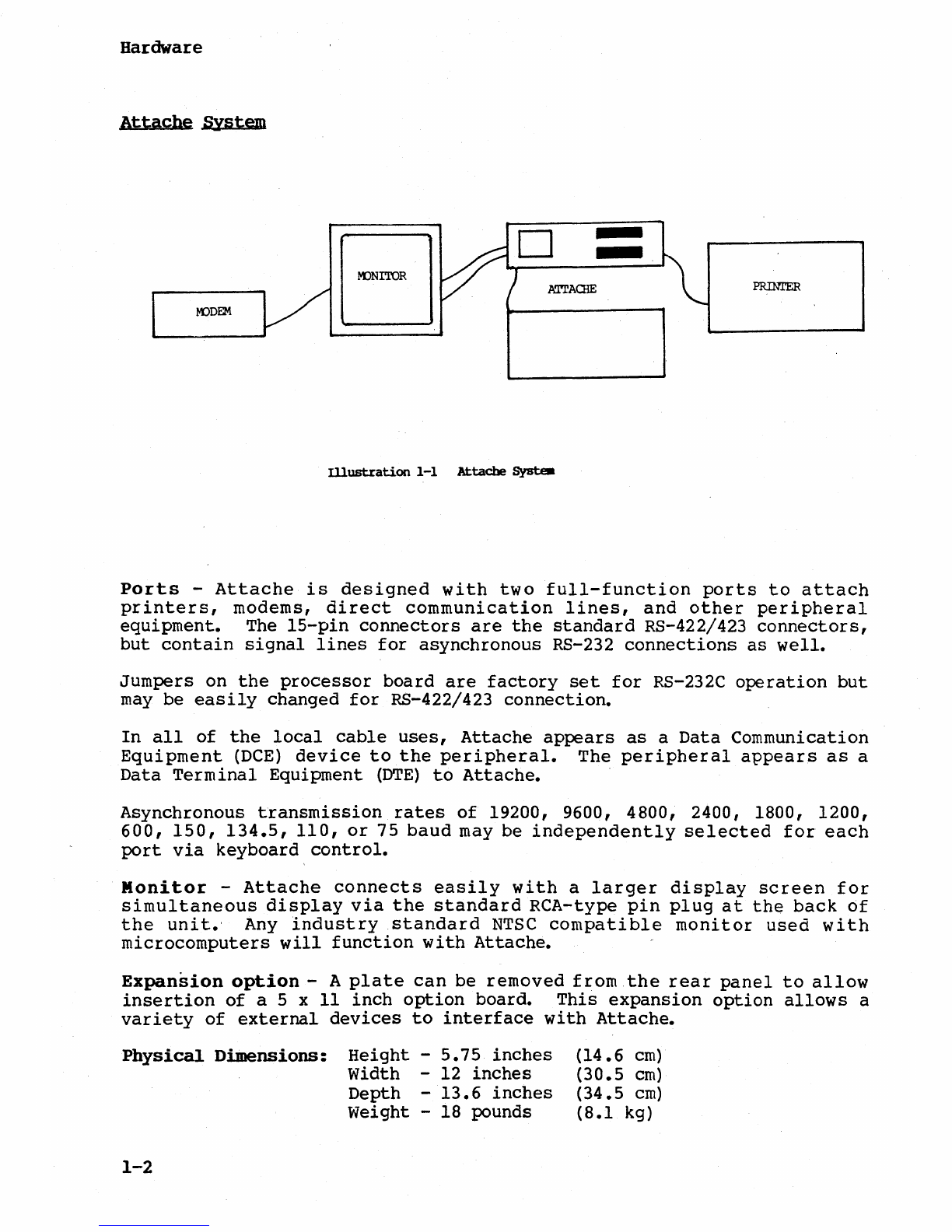
Hardware
Attache
System
EJ
D
--
--
PRINl'ER
lllustration
1-1
Attache
5ysteII
Ports
-
Attache
is
designed
with
two
full-function
ports
to
attach
printers,
modems,
direct
communication
lines,
and
other
peripheral
equipment.
The
IS-pin
connectors
are
the
standard
RS-422/423
connectors,
but
contain
signal
lines
for
asynchronous RS-232
connections
as
well.
Jumpers
on
the
processor
board
are
factory
set
for
RS-232C
operation
but
may
be
easily
changed
for
RS-422/423
connection.
In
all
of
the
local
cable
uses,
Attache
appears
as
a
Data
Communication
Equipment
(DCE)
device
to
the
peripheral.
The
peripheral
appears
as
a
Data
Terminal
Equipment
(DTE)
to
Attache.
Asynchronous
transmission
rates
of
19200, 9600, 4800, 2400, 1800, 1200,
600,
150,
134.5,
110,
or
75
baud
may be
independently
selected
for
each
port
via
keyboard
control.
Monitor
-
Attache
connects
easily
with
a
larger
display
screen
for
simultaneous
display
via
the
standard
RCA-type
pin
plug
at
the
back
of
the
unit.,
Any
industry
standard
NTSC
compatible
monitor
used
with
microcomputers
will
function
with
Attache.
Expansion
option
- A
plate
can
be
removed
from
the
rear
panel
to
allow
insertion
of
a 5 x 11
inch
option
board.
This
expansion
option
allows
a
variety
of
external
devices
to
interface
with
Attache.
Physical
Dimensions:
Height
-
5.75
inches
width
-12
inches
Depth -
13.6
inches
Weight -18 pounds
1-2
(14.6
cm)
(30.5
cm)
(34.5
cm)
(8.1
kg)
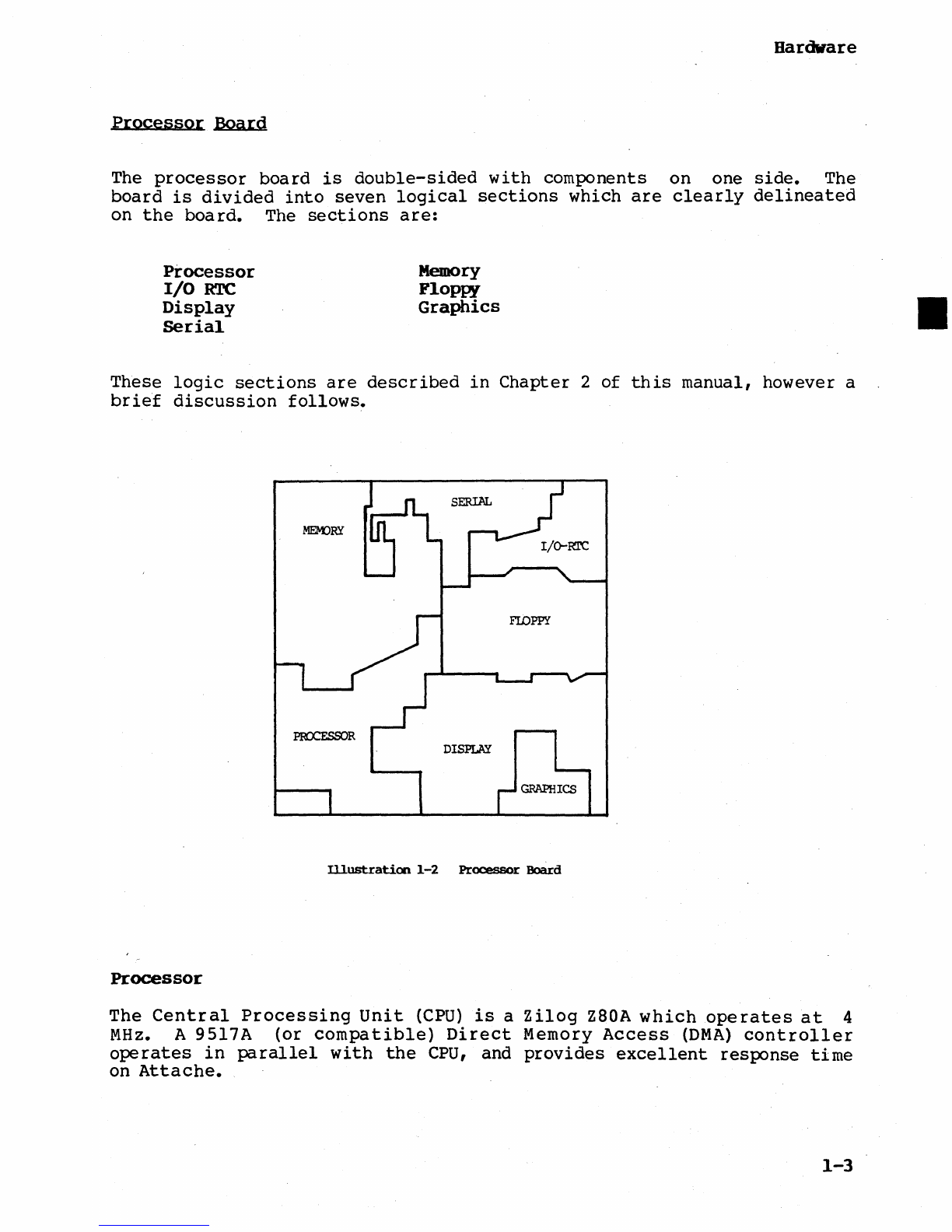
Hardware
Processor
Board
The
processor
board
is
double-sided
with
components
on
one
side.
The
board
is
divided
into
seven
logical
sections
which
are
clearly
delineated
on
the
board.
The
sections
are:
Processor
I/O
RTC
Display
Serial
Memory
Floppy
Graphics
These
logic
sections
are
described
in
Chapter
2
of
this
manual, however a
brief
discussion
follows.
POCCESSOR
DISPLAY
lllustratioo
1-2
Processor
Board
Processor
The
Central
Processing
Unit
(CPU)
is
a
Zilog
Z80A
which
operates
at
4
MHz.
A
95l7A
(or
compatible)
Direct
Memory
Access
(DMA)
controller
operates
in
parallel
with
the
CPU,
and
provides
excellent
response
time
on
Attache.
1-3
•

Hardware
Memory
The memory
provides
the
user
64K
(65,536)
bytes.
A
4K
byte
Read-Only
Memory
chip
(ROM)
contains
the
Terminal
EmUlation
routine,
the
Monitor
Mode,
diagnostic
programs, and
pointers
to
the
CP/M
load
routines.
The
ROM
is
mapped
in
and
out
of
main
memory,
so
the
entire
64K
bytes
of
memory
is
user
accessible.
I/O
RTC
(Real-Time Clock)
Input/Output
is
designed
for
maximum
throughput
with
m~n~mum
response
time.
Attache
uses
a
Z80
PIO
for
efficient
interface
between
the
system
and
the
keyboard,
the
RTC,
the
sound
effects
generator,
and
the
CMOS
Random
Access
f.'lemory
chip
(RAM).
A
battery
powered
OK!
MSM5832
(or
equivalent)
RTC
performs
continuous
time
of
day and
date
functions.
The
AY-3-89l2
Sound
Chip
is
user
programmable.
The
chip
drives
the
speaker
which
emits
key
click
sounds,
alarms
and
additional
programmable
audio
feeaback.
A 5101
CMOS
RAM
stores
system
parameters,
such
as
keyboard
volume,
key
sounds,
baud
rates,
etc.,
which
may
be programmed
via
the
keyboard.
Floppy
Disk
Attache
uses
a
D765A
Floppy
Disk
Controller
chip.
Data
transfers
are
handled
by
the
Direct
Memory
Access
controller.
High
reliability,
a
wide
range
of
capability,
and maximum
throughput
are
provided
with
this
method
of
disk
control.
Display
A
CRT
5027
controller
chip
provides
control
for
the
various
display
attributes
and
capabilities
which
are
generated
in
this
section
of
the
processor
board.
The
display
section
contains
4K
bytes
of
alphanumeric
display
Random
Access
Memory
(RAM).
Gr:aphics
The
graphics
control
and
10K
bytes
of
graphics
memory
for
the
320
dot
wide
by
240
dot
high
screen
are
contained
in
this
area.
1-4

Hardware
Serial
The
Z80
Serial
Input/Output
controller
(SID)
handles
two
independent
full-duplex
ports
with
separate
control
and
status
lines.
These
ports
may
be
used
to
attach
printers
or
modems
to
the
system.
By
setting
the
jumpers
within
the
system,
Attache
can be
configured
for
RS-232,
-422,
or
-423.
Attache
CP/M
configures
the
SID
software
for
commonly used asynchrorious
protocol.
The
system
is
delivered
with
jumpers
installed
for
the
popular
•
RS-232C
interface.
This
serial
interface
is
used
by
virtually
every
serial
peripheral
manufactured.
By
changing
the
standard
jumper
settings,
Attache's
AM26LS30
drivers
and
AMLS2632
receivers
use RS-422 and -423
standards.
These
interfaces
allow
transmissions
at
very
high
baud
rates
for
long
distances
(up
to
10,000
feet
in
some
cases)
with
low-cost
wiring.
Expansion OpCion
An
internal
connector
will
interface
with
the
system
bus.
This
allows
a
variety
of
external
devices
to
interface
with
Attache.
DisplAY
Attache
contains
a
high-resolution
display
designed
for
personal
viewing
distance.
Alphanumeric
Display
The S.Sft
diagonal
display
is
24
lines
of
80
characters
each.
Attache's
display
optimizes
user
efficiency
with
software
selectable
features,
such
as
double
size
characters
and
multiple
character
sets.
The
entire
screen
can
be
updated
in
as
little
as
1/60thof
a second.
Display
attributes
greatly
enhance
the
display
effectiveness.
Attache
has
all
of
the
following
standard
capabilities:
Reverse
image
Boldface
Underline
Strikethrough
Subscript
Superscript
Double
size
Highlight
1-5
Hardware
Graphic
Display
-
Attache
handles
the
requirements
of-
computer
graphics
with
a
very
high-
resolution
display.
This
is
accomplished
with
a 320
dot
wide by 240
dot
high
display.
Attache's
resolution
provides
+/-
.25%
accuracy
in
the
vertical
scale,
with
even
greater
accuracy
horizontally.
Text
information
is
easily
presentee
along
with
the
graphics
for
a
"complete"
display.
Diskette
Drjyes
Attache
contains
two
5-1/4"
mini-floppy
diskette
drives.
The
drives
use
a
direct
drive
motor
for
fast
response,
highly
accurate
data
transfer,
and
very
high
reliability.
The
two
drives
are
shock-mounted
in
the
disk
drive
module
assembly.
The
,module
has
two
separate
cables
and
modular
connectors;
one
for
data
transfers
and one
for
powering
the
drives.
Attache
responds
quickly
to
shut-down
the
drives
after
the
data
has
been
transferred.
This
approach
prolongs
media
life
substantially,
while
minimizing
usage
of
the
drives
themselves.
The
drives
are
up-to-speed
and
transferring
data
in
less
than
.5
seconds.
Standard
Format
The
drives
are
formatted
for
CP/M
usage on
the
Attache
with
360K
bytes
of
user
storage.
The
data
is
formatted
with
512
bytes
per
sector,
10
sectors
per
track,
46
tracks
on
the
top
side,
50
tracks
on
the
bottom.
Some
data
space
is
reserved
for
CP/M
and
directories,
leaving
360K
bytes
of
storage.
1-6
Hardware
Keyboard
The
Attache
keyboard
is
a
full
alphanumeric
key
set
laid
out
in
the
IBM
Selectric
tm
keyboard
configuration.
Additionally,
cursor
movement,
delete,
and
multi-function
keys
are
located
on
the
keyboard.
A 16
keystroke
buffer
handles
the
burst
speed
that
can
occur
with
short
words. The key
stroke
speed
capability
is
calculated
at
approximately
60
key
strokes
per
second,
or
720 words
per
minute.
All
keys
will
enter
an
auto-repeat
mode
if
depressed
for
more
than
1/2
second.
This
allows
the
user
efficient
data
entry
and
system
control
capability.
The
repeat
speed
during
auto-repeat
is
easily
adjusted,
on
the
rear
of
the
keyboard,
to
the
optimum needs
of
each
user.
The
audible
feedback
of
the
keys
are
adjustable
via
Set-up
Mode's
"volume" and
"click"
options.
The
keyboard's
construction
makes
the
keys
virtually
impervious
to
contamination.
The
keyboard
is
designed
to
connect
to
the
system
iri a
modular
fashion.
The
connector
on
the
system
and
the
keyboard
uses
a
telephone-style,
4-
wire
modular
connector.
A
standard
phone
coil
cord
can
be
used
to
provide
up
to
10
feet
of
keyboard
distance.
Multi-Function
Keys
Keys on
the
top
row
of
the
keyboard
are
used
to
perform
several
functions
in
addition
to
numeric
and
special
character
typewriter
functions.
Multi-functions
are
activated
by
pressing
two
or
more
keys
at
the
same
time,
as
instructed
by
the
keyboard
template.
The
keys
which
activate
the
multi-functions
are
the
CTRL
key,
SHIFT
and
CTRL
keys,
and C'l'RL and
ESC
keys.
lO-Key
Mode
The
Attache
keyboard
may
be
used
as
a 10-Key pad
for
entering
columns
of
figures.
Certain
letter
keys
are
converted
to
numbers when 10-Key
Mode
is
activated
and
the
letter
keys
are
used
in
lower
case.
10-Key
Mode
is
activated
by
pressing
CTRL
and
CAPS
LOCK
simultaneously.
Press
CAPS
LOCK
to
return
to
upper
case,
or
press
CTRL
and
CAPS
LOCK
simultaneously
to
return
to
lowercase.
.1-7
•

Hardware
Power
SuP1>ly
The power
supply
contains
built-in
self-checking
circuitry
and
indicator
lights
to
verify
proper
operation.
A
thermistor
controlled,
DC
brushless
motor
fan
is
contained
~n
the
power
supply
module
to
provide
cooling
for
Attache.
The
fan
runs
quietly,
and
causes
no
electronic
noise
that
could
interfere
with
system
operation.
The
constant
internal
temperature
provides
consistent
trouble-free
operation
as
well
as
reducing
component
degradation.
The power
supply
operates
from
95
to
135
volts
or
190
to
270
volts
with
a
frequency
range
of
48
to
440
Hz.
Attache
may be
operated
anywhere
in
the
world
by
setting
the
voltage
selector
card
and
with
use
of
the
correct
power
cord
or
international
adapter.
Setting
the
Voltage
1.
Remove
the
fuse.
2.
Remove
the
printed
circuit
board
at
the
base
of
the
fuse
box.
3.
Turn
the
card
so
the
required
voltage
setting
(100,
120,
220,
or
240)
is
facing
you.
4.
Reinstall
the
printed
circuit
board
in
the
fuse
box
with
the
desired
setting
facing
you.
5.
Reinstall
the
fuse;
use
either
Slo-Blo
2A
l15V
or
Slo-BLo
lA
230V, depending on
your
voltage
selection.
Where
conventional
power
is
not
available,
the
DC
power
option
allows
instant
operation
from 10
to
16
volt
automobile
or
marine
batteries,
20
to
32
volt
aircraft
systems,
or
from
portable
battery
packs.
1-8
Other manuals for ATTACHE
1
Table of contents
Other OTRONA Laptop manuals


