ozQRP MDT Instructions for use

MDT Construction Manual –Issue 2 Page 1
MDT
DSB TRANSCEIVER
CONSTRUCTION MANUAL

MDT Construction Manual –Issue 2 Page 2
CONTENTS
1Introduction..............................................................................................................................................................4
2DSB vs SSB .................................................................................................................................................................5
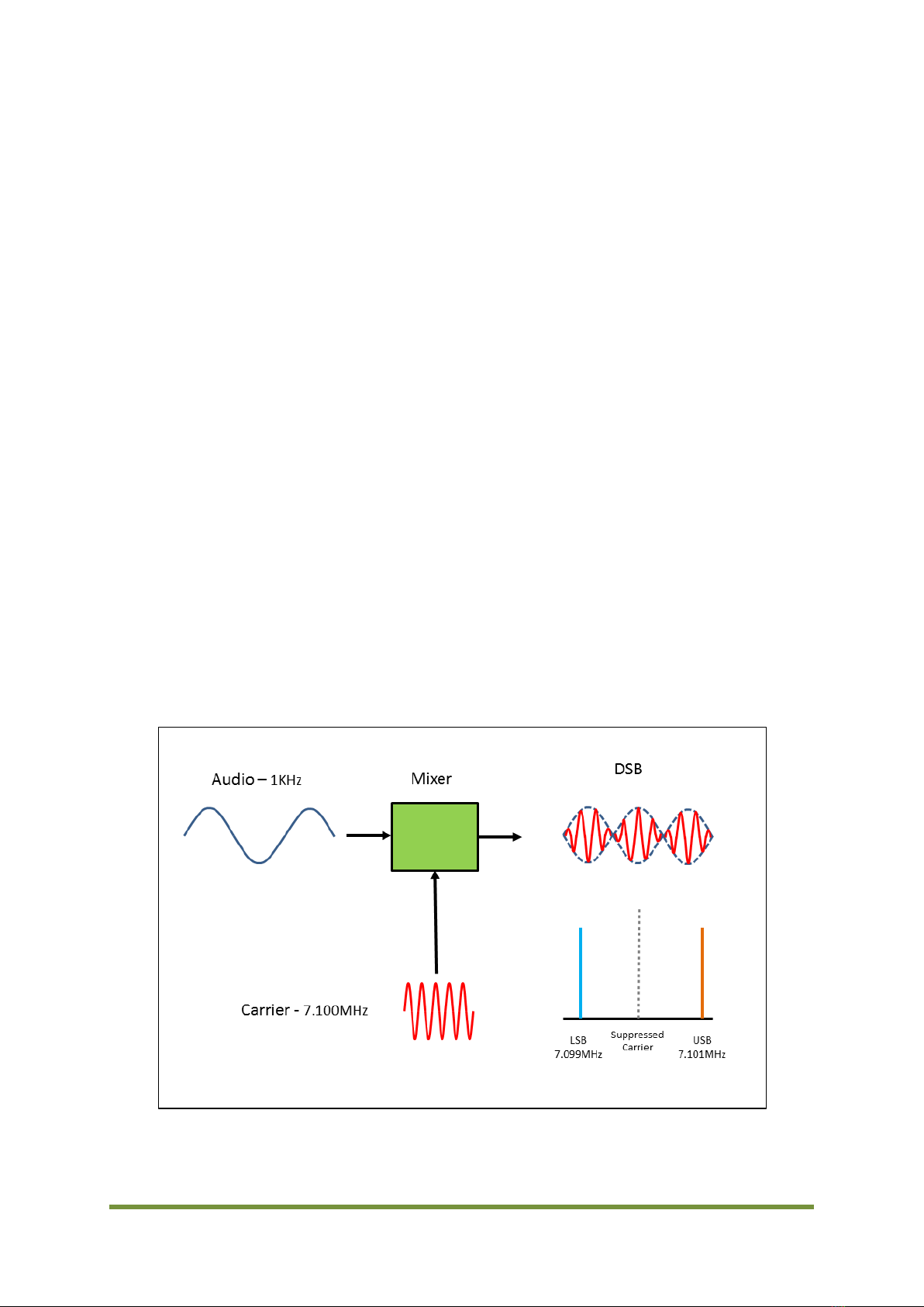
3DSB transmitter.......................................................................................................................................................6
4Direct Conversion receiver................................................................................................................................. 7
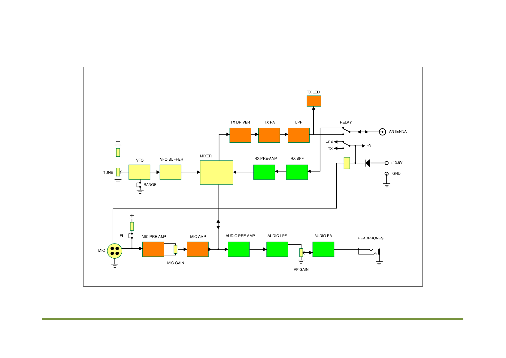
5MDT Block Diagram...............................................................................................................................................8
6Circuit Description .................................................................................................................................................9
6.1 Variable Frequency Oscillator (VFO)........................................................................................................................9
6.2 Mixer .......................................................................................................................................................................................9
6.3 Microphone amplifier ................................................................................................................................................... 10
6.4 Transmit amplifier......................................................................................................................................................... 10
6.5 Power Supply and RX/TX switching ...................................................................................................................... 11
6.6 Receive audio.................................................................................................................................................................... 11
7Kit Supplied Parts ................................................................................................................................................ 17
8Individual Parts List............................................................................................................................................ 19
9Construction........................................................................................................................................................... 21
9.1 General ................................................................................................................................................................................ 21
9.2 Building the PCB.............................................................................................................................................................. 22
10 Final Assembly...................................................................................................................................................... 33
10.1 Microphone socket......................................................................................................................................................... 33
10.2 Terminating plugs .......................................................................................................................................................... 34
10.3 Front Panel ........................................................................................................................................................................ 35
10.4 Mounting the PCB........................................................................................................................................................... 35
11 Testing and alignment ....................................................................................................................................... 36
11.1 General ................................................................................................................................................................................ 36
11.2 Power on............................................................................................................................................................................. 36
11.3 Receive ................................................................................................................................................................................ 36
11.4 Transmit ............................................................................................................................................................................. 37
11.5 Marking the VFO scale.................................................................................................................................................. 38
12 Modifications......................................................................................................................................................... 40
12.1 Setting the VFO range ................................................................................................................................................... 40
12.2 Receiver alignment ........................................................................................................................................................ 40
12.3 Crystal operation ............................................................................................................................................................ 40
12.4 Using a loudspeaker ...................................................................................................................................................... 40
13 Operation................................................................................................................................................................. 41
13.1 Setting up ........................................................................................................................................................................... 41
13.2 Receiving ............................................................................................................................................................................ 41
13.2.1 SSB.......................................................................................................................................................... 41
13.2.2 CW........................................................................................................................................................... 41
13.3 Transmitting ..................................................................................................................................................................... 42

MDT Construction Manual –Issue 2 Page 3
List of Figures
Figure 1 DSB generation................................................................................................................................................6
Figure 2 Direct Conversion receiver.........................................................................................................................7
Figure 3 MDT Block diagram.......................................................................................................................................8
Figure 4 Carrier oscillator.......................................................................................................................................... 12
Figure 5 Mixer................................................................................................................................................................. 13
Figure 6 Microphone Amplifier ............................................................................................................................... 14
Figure 7 Transmit.......................................................................................................................................................... 15
Figure 8 Receive Audio................................................................................................................................................ 16
Figure 9 Diode identification.................................................................................................................................... 22
Figure 10 DIP ICs ........................................................................................................................................................... 23
Figure 11 Relay install................................................................................................................................................. 23
Figure 12 Non-polarised capacitors ...................................................................................................................... 24
Figure 13 LPF capacitor marking............................................................................................................................ 24
Figure 14 Trimcap install........................................................................................................................................... 25
Figure 15 BD139 location .......................................................................................................................................... 25
Figure 16 BD139 lead identification...................................................................................................................... 26
Figure 17 LED lead bending...................................................................................................................................... 27
Figure 18 LED install.................................................................................................................................................... 27
Figure 19 Pot with tab removed.............................................................................................................................. 31
Figure 20 Component overlay.................................................................................................................................. 32
Figure 21 Mic connector wiring .............................................................................................................................. 33
Figure 22 Typical circuit voltages........................................................................................................................... 39
Figure 23 DSB transmit waveform......................................................................................................................... 42
Change History
Date
Issue
Comments
12-6-15
1
First release
20-6-15
2
Corrected values for R43 and C13, and other minor typos.

MDT Construction Manual –Issue 2 Page 4
1INTRODUCTION
The MDT (Minimalist Double Sideband Transceiver) is an inexpensive and easy to build kit for
the 40M band. It is ideal for the first time builder as all parts except the microphone socket are
mounted on a single PCB and all the components are through hole. There is a SMD tuning diode
but this comes pre-installed. The PCB is a high quality double sided type with ground plane,
solder mask and silk screen.
The plastic case is small and lightweight and can easily be held in one hand. The front and rear
panels, which are made of PCB material, come pre-cut and feature silkscreened labeling.
The low receive current of the MDT means it is ideal for battery operation. The transmitter
outputs between 1.5 and 2 watts DSB which is ample for short distance contacts through the
day and long distance contacts under good conditions. DSB transmissions are entirely
compatible with SSB transceivers, and in fact most operators won’t be aware unless you tell
them.
Building the MDT is quick and easy. The receiver doesn’t require any alignment and the only
setup required for the transmitter is setting the microphone gain and balancing the mixer to
null out the carrier.
A kit of parts for the MDT including everything you need, such as enclosure and front and rear
panels is available from www.ozQRP.com.
MDT Specifications and features:
1. Size 130mm x 100mm x 50mm.
2. Direct Conversion receiver. Sensitivity 0.4uV for 10dB S+N/N.
3. Double Sideband transmitter. Nominal 1.5W output. Up to 2W depending on power
supply voltage.
4. Selectable frequency range. 7.090MHz - 7.130MHz or 7.050MHz - 7.110MHz.
5. Microphone amplifier accepts standard low impedance dynamic or Electret microphone
with selectable on-board bias resistor.
6. LED transmit power and modulation indicator.
7. 3.5mm stereo headphone connector. Can power external loudspeaker.
8. Carrier suppression up to 50dB.
9. All spurious transmit outputs better than -46dBC.
10. Receive current approximately 50mA.
11. Transmit current approximately 250mA at maximum power output.
12. Reverse polarity protection using a series-diode.

MDT Construction Manual –Issue 2 Page 5
2DSB VS SSB
Why DSB? The answer is simple. A DSB transceiver is less expensive, less complicated and
easier to build and align than a SSB transceiver. This is due mainly to a DSB transceiver not
having a crystal filter, IF amplifier and multiple mixers that are required in a SSB design. Note
that in a DSB transceiver the receiver is more often referred to as a Direct Conversion (DC)
receiver.
For the first time builder or for a small and cheap rig, DSB is ideal. Over the years countless
amateurs have started out this way.
While a DSB rig has many advantages for the home builder, there are some things to consider.
Firstly, a DSB transmitter occupies twice the bandwidth of a SSB transmitter. On a quiet band
this does not cause any problems but on a crowded band it may not be as easy to find a free spot
to operate without interfering with nearby stations. Secondly, the Direct Conversion receiver
has equal response to both sidebands. This means you hear signals on both upper and lower
sidebands simultaneously. This results in a slightly higher noise level and the possibility of
hearing two separate stations at the same time.
There are, however, a couple of nice advantages when a Direct Conversion receiver is used with
a DSB transmitter. Firstly, you can operate with SSB stations using Upper Sideband (USB) or
Lower Sideband (LSB) without having to change controls or move frequency. Secondly, being
able to hear both sidebands means that you can check for other stations on both sides of your
frequency before transmitting and avoid interfering with them.

MDT Construction Manual –Issue 2 Page 6
3DSB TRANSMITTER
Figure 1 shows how a Double Sideband signal is generated. The mixer used here is not to be
confused with an audio mixer that combines, for example, microphones. The mixer here is more
correctly called a multiplier, where the inputs are multiplied in the same way as in a
mathematical equation. When multiplying sine waves there are two main outputs and these are
the sum and difference of the frequencies of the input signals.
The first input to our mixer is from the VFO or carrier oscillator. The second input is audio from
the microphone amplifier.
The dominant outputs of the mixer are the sum and difference frequencies, that is, the sum and
difference of the carrier and audio frequencies. In this case, 7.101MHz (7.100MHz + 1KHz)
upper sideband, and 7.099MHz (7.100MHz –1KHz) lower sideband.
The important thing to note is that only the sidebands are present at the output of the mixer as
the carrier and audio signals have been suppressed by the action of the balanced mixer.
The diagram in Figure 1 at top right shows the DSB output signal in the time domain, or how it
would be seen on an oscilloscope. Note the overlapping envelope shape that follows the audio
waveform. The diagram at bottom right shows the DSB output signal in the frequency domain
and how it would be seen on a spectrum analyser. The horizontal axis is frequency and the
vertical axis is amplitude. The dotted vertical line in the middle indicates the suppressed carrier
frequency.
By contrast, if this was a SSB transmitter, there would be a crystal filter placed after the mixer
and one of the sidebands would be filtered out. However, it would then be necessary to add
another mixer to move the SSB signal onto the wanted transmit frequency.
Figure 1 DSB generation

MDT Construction Manual –Issue 2 Page 7
4DIRECT CONVERSION RECEIVER
Figure 2 shows the simplified diagram of a Direct Conversion receiver. As with a DSB generator
the mixer has two inputs and an output, but this time the signal directions are reversed.
Signals from the antenna are presented to the mixer, and mixed with the VFO signal. The output
again contains sum and difference signals. The sum frequency of 7.101MHz + 7.100MHz
(14.201MHz) is easily filtered out by a low pass audio filter. However the difference frequency
of 7.101MHz –7.100MHz (1KHz) can pass through the filter and be heard in the headphones.
This is the upper sideband response as the antenna signal frequency of 7.101MHz is above the
7.100MHz VFO frequency.
Note that there is also another antenna signal that can be heard. This is the lower sideband
signal at 7.099MHz. This would also produce a 1KHz tone in the headphones.
This ability to simultaneously detect both upper and lower sidebands is an important
characteristic of a Direct Conversion receiver.
Both Figure 1 and Figure 2 show a single 1KHz tone for the audio signal. This is done to make it
easier to understand the process involved. In practice there would be a range of voice band
frequencies present, but the same mixing conversion principle applies.
Figure 2 Direct Conversion receiver

MDT Construction Manual –Issue 2 Page 8
5MDT BLOCK DIAGRAM
Figure 3 MDT Block diagram

MDT Construction Manual –Issue 2 Page 9
6CIRCUIT DESCRIPTION
6.1 VARIABLE FREQUENCY OSCILLATOR (VFO)
Transistor Q1 is configured as a Colpitts oscillator and acts as the carrier oscillator in transmit
and beat frequency oscillator (BFO) in receive. The frequency is set predominantly by a ceramic
resonator (X1) and a dual variable capacitance (varicap) diode D1. The capacitance of D1 is
altered by a varying the DC voltage applied to the Cathodes through the Tune control VR1 and
R3. To help stabilize the oscillator and minimize frequency drift the power supply to the
oscillator and the Tune control is regulated with a 9.1V Zener diode ZD1.
The VFO has effectively two ranges through the Range link. If the link is closed both varicap
diodes are in parallel circuit and the tuning range is approximately 60KHz. With the link open,
only one varicap diode is in use and the range change is reduced to around 40KHz. Capacitor C3
is not normally used.
The oscillator signal is fed to the emitter follower buffer stage Q2 via a small capacitor (C6). The
buffer stage provides light loading of the oscillator and a low impedance drive for the mixer.
6.2 MIXER
The balanced mixer is a diode switching type and doubly balanced. It performs two functions. In
TX mode it mixes the VFO carrier signal with the microphone audio signal to produce DSB while
in RX mode it mixes the antenna signal with the VFO signal to produce received audio.
The carrier signal, which is much larger in amplitude than the audio signal, is applied
simultaneously to both sides of the mixer through trimpot VR2. The carrier signal turns on the
diodes to form a low resistance and is why it is referred to as a switching mixer. As the carrier is
capacitively coupled it swings both positive and negative around ground potential. When the
carrier is positive, current flows through diodes D2 and D5 causing them to conduct and
become a low resistance. When the carrier goes negative diodes D3 and D4 conduct. Note that
capacitor C10 holds the junction of D2 and D4 at ground for RF. As the currents are equal
through each of the conducting diodes the differential voltage across winding one of T1 does not
change and no RF is present at winding three, the output of T1. If an audio signal is injected into
the bridge at the junction of D2 and D4 the mixer balance is upset because the audio changes
state much less frequently than the carrier signal and the instantaneous diode currents are not
equal. As a result a signal is now output on winding three of T1, which is a double sideband
suppressed carrier waveform.
Due to variations in component parameters the mixer balance is not exact and if not
compensated for the carrier balance would be poor. Trimmer capacitor TC1 and C9 are used to
equalize the capacitance on the mixer sides, while trimpot VR2 is used to balance the diode
currents in each side. They are adjusted together to bring the modulator into balance. In
practice up to 50dB of carrier suppression can be achieved.

MDT Construction Manual –Issue 2 Page 10
Received signals from the antenna are fed to a broadly tuned band pass filter formed with L1,
C14 and C15. The values of C14 and C15 are selected to form a tuned circuit with L1 at 7MHz.
The ratio of C14 and C15 provide impedance matching between the tuned circuit and the 50
ohm antenna source. It also sets the loaded ‘Q’ of the tuned circuit and as a result the overall
filter bandwidth. The filter is connected to the receive pre-amplifier via a small 100pF coupling
capacitor (C13). The pre-amplifier stage is formed around transistor Q3 in a common emitter
configuration and provides around 10 times amplification. The collector load is winding two of
the mixer transformer T1, and here the signal is mixed with the carrier. The resultant audio
appears at the junction of D2 and D4.
6.3 MICROPHONE AMPLIFIER
Transistor Q7 is the microphone pre-amplifier with an input impedance of around 10K ohm and
a gain of around 40 set mainly by C34 and R28. C32 is included across the input to prevent RF
feeding into the amplifier. The amplified output appears across the 5K ohm trimpot (VR3) in the
collector. This becomes a pre-set microphone gain control, and the signal from the wiper is fed
to the microphone amplifier stage Q8. This stage only has a gain of around 3, but it’s biased for
higher current and a low value collector resistor so it can drive the balanced modulator. C33 and
C36 provide heavy low pass filtering to limit the transmitted bandwidth.
If an Electret microphone is used, R25 provides a DC bias current and is enabled by shorting the
EL link. If a dynamic microphone is used the link is left open.
6.4 TRANSMIT AMPLIFIER
Transmit signal from the mixer is applied to the driver stage built around transistor Q4. A
BD139 works well here when biased with about 50mA of collector current. The design is well
proven using both shunt and series feedback to provide low input and output impedance and
good stable gain on the low HF bands.
The power amplifier stage is formed from two BD139 transistors (Q5 and Q6) in parallel. They
operate in class B and provide up to 2 Watts PEP of power from a 13.8 V supply. The bases of
the transistors are held at around 0.6 volts DC by the voltage reference formed by R18 and
diode D6. This holds the transistors at or just below the point of conduction and so draw very
little current with no RF drive. The 1.5 ohm resistors in the emitters force the transistors to
share the load more equally, and provide a small amount of negative feedback which improves
stability and prevents thermal runaway.
The collector load for Q5 and Q6 is a toroidal inductor L2. The specified inductance was found to
provide maximum output into the low pass filter. The waveform from Q5 and Q6 can be high in
harmonics and so a 5 pole low pass filter is included to reduce the level of harmonic and other
spurious energy to an acceptable level. L4 and a 150pF capacitor form a parallel tuned circuit to
give sharp attenuation of the second harmonic.
As a visual indication of power output and modulation, the transmit signal is sampled by
capacitor C28 and ground referenced by R21. The signal is rectified by D9 and filtered by C29.
This drives the front panel LED via current limiting resistor R22.

MDT Construction Manual –Issue 2 Page 11
6.5 POWER SUPPLY AND RX/TXSWITCHING
When the PTT is operated the TX/RX relay is energized and the transmit signal is passed to the
antenna. When the PTT is not operated the relay switches the antenna through to the receive
circuits. The relay also switches power to the TX and RX sections as required
Diode D8 provides reverse polarity protection. With the power supply connected with the right
polarity, D8 will pass current onto the board. There is a small voltage drop of about 0.3 volts but
this has minimal effect on transmitter performance. If the supply is connected in reverse D8
will not conduct and the board will be protected.
6.6 RECEIVE AUDIO
The low level audio signal from the mixer is applied to the audio pre-amplifier stage (U1A). This
is formed from one half of an LM833 dual low noise op-amp and has a gain of around 100 or
40dB. A reference supply for the non-inverting input is obtained from R33, R35 and C40. The
high frequency response of U1A is limited by C41. The output of U1A is DC coupled to the 2 pole
low pass filter (U1B) with a 3dB cutoff frequency of 2400Hz. This stage has only unity gain but
its main task is to set the receiver bandwidth.
The output of the low pass filter is coupled to the AF gain control VR4 via a 1uF capacitor (C44).
A LM386 (U2) is used to boost the signal from the AF gain control to drive a set of headphones.
The gain is set by C47 and R42 to about 50 times or 34dB, while resistor R43 limits the audio to
a comfortable level for headphone listening. If an external low impedance speaker is used
instead of headphones, then R43 can be replaced with a link.
A MOSFET (Q9) is turned on in TX mode and shorts the audio signal to ground. Even though the
audio amplifiers are switched off during transmit, this is still necessary because microphone
signals can make their way through to the headphones while the audio amplifiers are turning
off.

MDT Construction Manual –Issue 2 Page 12
Figure 4 Carrier oscillator

MDT Construction Manual –Issue 2 Page 13
Figure 5 Mixer

MDT Construction Manual –Issue 2 Page 14
Figure 6 Microphone Amplifier

MDT Construction Manual –Issue 2 Page 15
Figure 7 Transmit

MDT Construction Manual –Issue 2 Page 16
Figure 8 Receive Audio

MDT Construction Manual –Issue 2 Page 17
7KIT SUPPLIED PARTS
QTY
Value
Designator
Capacitors
3
22pF ceramic disc NPO
C6, C9, C28
2
56pF ceramic disc NPO
C4, C5
1
100pF ceramic disc
C13
1
150pF 100V C0G ceramic MLCC
C24
1
220pF ceramic disc
C41
1
220pF 100V C0G ceramic MLCC
C23
1
470pF ceramic disc
C14
3
470pF 100V C0G ceramic MLCC
C25, C26, C27
2
1nF ceramic disc
C15, C32
1
4.7nF polyester MKT
C43
4
10nF polyester MKT
C10, C33, C42, C46
1
47nF polyester MKT
C51
2
100nF polyester MKT
C31, C38
14
100nF ceramic MLCC
C1, C2, C7, C8, C11, C12, C16, C17, C18, C19, C20, C22,
C29, C36
4
1uF 50V RB electrolytic
C35, C37, C44, C45
3
10uF 25V RB electrolytic
C34, C47, C48
6
100uF 25V RB electrolytic
C21, C30, C39, C40, C49, C50
1
40pF trim capacitor
TC1
Resistors
2
1.5Ω1/4W 5%
R19, R20
4
10Ω 1/4W 5%
R13, R16, R41, R44
2
22Ω1/4W 5%
R17, R43
4
100Ω1/4W 5%
R7, R23, R28, R31
1
220Ω 1/4W 5%
R1
7
470Ω1/4W 5%
R8, R11, R15, R24, R27, R32, R42
3
1K 1/4W 5%
R2, R5, R30
4
2.2K 1/4W 5%
R9, R12, R14, R21
1
3.3K 1/4W 5%
R18
4
4.7K 1/4W 5%
R22, R25, R34, R39
5
10K 1/4W 5%
R10, R33, R35, R37, R38
1
56K 1/4W 5%
R6
2
100K 1/4W 5%
R3, R4
2
220K 1/4W 5%
R29, R40
2
470K 1/4W 5%
R26, R36
1
500Ωvertical multi-turn trimpot
VR2
1
5K horizontal trimpot
VR3
1
10K LOG 16mm pot
VR4
1
50K LIN 16mm pot
VR1

MDT Construction Manual –Issue 2 Page 18
QTY
Value
Designator
Semiconductors
1
SVC236 dual varicap diode
D1
6
1N4148 signal diode
D2, D3, D4, D5, D9, D10
2
1N4004 1A power diode
D6, D7
1
1N5819 1A Schottky diode
D8
1
9.1V 500mW Zener
ZD1
5
2N3904 NPN transistor
Q1, Q2, Q3, Q7, Q8
3
BD139 NPN transistor
Q4, Q5, Q6
1
2N7000 MOSFET
Q9
1
LM833 dual op-amp
U1
1
LM386/4 audio power amp
U2
1
7.2MHz ceramic resonator
X1
1
5mm blue LED
LED1
Coils
1
FT37-43 4T:8T:4T
T1
1
FT37-43 8T:2T
T2
1
FT50-43 8T
L2
1
T50-2 15T
L1
1
T50-2 14T
L3
1
T50-2 11T
L4
Hardware
1
BNC RA PCB mount connector
ANT
1
3.5mm stereo PCB mount socket
PHONES
1
12V DPDT DIP relay
K1
1
2.1mm DC PCB mount socket
PWR
2
2 pin 2.54mm pitch header
MIC, PTT
2
2 pin 2.54mm pitch plug with pins
MIC, PTT
1
2M 0.4mm enamelled wire
-
1
0.4M hookup wire
-
1
Plastic instrument case including
screws
-
1
MDT Front panel
-
1
MDT Rear panel
-
2
Knobs
-
1
4 pin mic socket
-

MDT Construction Manual –Issue 2 Page 19
8INDIVIDUAL PARTS LIST
Desig.
Value
Type
Desig.
Value
Type
ANT
-
PCB mount RA BNC
C44
1uF
50V RB electrolytic
C45
1uF
50V RB electrolytic
C1
100nF
ceramic MLCC
C46
10nF
polyester MKT
C2
100nF
ceramic MLCC
C47
10uF
25V RB electrolytic
C3
-
Not used. See text
C48
10uF
25V RB electrolytic
C4
56pF
ceramic disc NPO
C49
100uF
25V RB electrolytic
C5
56pF
ceramic disc NPO
C50
100uF
25V RB electrolytic
C6
22pF
ceramic disc NPO
C51
47nF
polyester MKT
C7
100nF
ceramic MLCC
C8
100nF
ceramic MLCC
D1
SVC236
Dual Varicap
C9
22pF
ceramic disc NPO
D2
1N4148
Signal diode
C10
10nF
polyester MKT
D3
1N4148
Signal diode
C11
100nF
ceramic MLCC
D4
1N4148
Signal diode
C12
100nF
ceramic MLCC
D5
1N4148
Signal diode
C13
100pF
ceramic disc NPO
D6
1N4004
1A power diode
C14
470pF
ceramic disc
D7
1N4004
1A power diode
C15
1nF
ceramic disc
D8
1N5819
1A Schottky diode
C16
100nF
ceramic MLCC
D9
1N4148
Signal diode
C17
100nF
ceramic MLCC
D10
1N4148
Signal diode
C18
100nF
ceramic MLCC
C19
100nF
ceramic MLCC
K1
-
PCB mount DIP signal relay
C20
100nF
ceramic MLCC
C21
100uF
25V RB electrolytic
L1
15T
T50-2 toroid
C22
100nF
ceramic MLCC
L2
8T
FT50-43 toroid
C23
220pF
100V C0G ceramic MLCC
L3
14T
T50-2 toroid
C24
150pF
100V C0G ceramic MLCC
L4
11T
T50-2 toroid
C25
470pF
100V C0G ceramic MLCC
LED1
-
5mm Blue LED
C26
470pF
100V C0G ceramic MLCC
C27
470pF
100V C0G ceramic MLCC
MIC
-
2 pin vertical header
C28
22pF
ceramic disc NPO
C29
100nF
ceramic MLCC
PHONES
-
PCB mount 3.5mm stereo socket
C30
100uF
25V RB electrolytic
PWR
-
PCB mount 2.1mm DC socket
C31
100nF
polyester MKT
PTT
-
2 pin vertical header
C32
1nF
ceramic disc
C33
10nF
polyester MKT
Q1
2N3904
NPN transistor
C34
10uF
25V RB electrolytic
Q2
2N3904
NPN transistor
C35
1uF
50V RB electrolytic
Q3
2N3904
NPN transistor
C36
100nF
ceramic MLCC
Q4
BD139
NPN transistor
C37
1uF
50V RB electrolytic
Q5
BD139
NPN transistor
C38
100nF
polyester MKT
Q6
BD139
NPN transistor
C39
100uF
25V RB electrolytic
Q7
2N3904
NPN transistor
C40
100uF
25V RB electrolytic
Q8
2N3904
NPN transistor
C41
220pF
ceramic disc
Q9
2N7000
N ch MOSFET
C42
10nF
polyester MKT
C43
4.7nF
polyester MKT

MDT Construction Manual –Issue 2 Page 20
Desig.
Value
Type
Desig.
Value
Type
R1
220Ω
1/4W 5% resistor
T1
4T:8T:4T
FT37-43 toroid
R2
1K
1/4W 5% resistor
T2
8T:2T
FT37-43 toroid
R3
100K
1/4W 5% resistor
R4
100K
1/4W 5% resistor
U1
LM833
Dual low noise op-amp
R5
1K
1/4W 5% resistor
U2
LM386-4
Audio power amp
R6
56K
1/4W 5% resistor
R7
100Ω
1/4W 5% resistor
VR1
50K
LIN 16mm potentiometer
R8
470Ω
1/4W 5% resistor
VR2
500Ω
Multi-turn trimpot
R9
2.2K
1/4W 5% resistor
VR3
5K
Horizontal trimpot
R10
10K
1/4W 5% resistor
VR4
10K
LOG 16mm potentiometer
R11
470Ω
1/4W 5% resistor
R12
2.2K
1/4W 5% resistor
X1
7.2MHz
ceramic resonator
R13
10Ω
1/4W 5% resistor
R14
2.2K
1/4W 5% resistor
R15
470Ω
1/4W 5% resistor
R16
10Ω
1/4W 5% resistor
R17
22Ω
1/4W 5% resistor
R18
3.3K
1/4W 5% resistor
R19
1.5Ω
1/4W 5% resistor
R20
1.5Ω
1/4W 5% resistor
R21
2.2K
1/4W 5% resistor
R22
4.7K
1/4W 5% resistor
R23
100Ω
1/4W 5% resistor
R24
470Ω
1/4W 5% resistor
R25
4.7K
1/4W 5% resistor
R26
470K
1/4W 5% resistor
R27
470Ω
1/4W 5% resistor
R28
100Ω
1/4W 5% resistor
R29
220K
1/4W 5% resistor
R30
1K
1/4W 5% resistor
R31
100Ω
1/4W 5% resistor
R32
470Ω
1/4W 5% resistor
R33
10K
1/4W 5% resistor
R34
4.7K
1/4W 5% resistor
R35
10K
1/4W 5% resistor
R36
470K
1/4W 5% resistor
R37
10K
1/4W 5% resistor
R38
10K
1/4W 5% resistor
R39
4.7K
1/4W 5% resistor
R40
220K
1/4W 5% resistor
R41
10Ω
1/4W 5% resistor
R42
470Ω
1/4W 5% resistor
R43
22Ω
1/4W 5% resistor
R44
10Ω
1/4W 5% resistor
Table of contents
Other ozQRP Transceiver manuals