ozQRP MST400 Instructions for use

MST Construction Manual –Issue 1 Page 1
MST
CONSTRUCTION MANUAL

MST Construction Manual –Issue 1 Page 2
CONTENTS
1Introduction..............................................................................................................................................................4
2Block Diagram..........................................................................................................................................................5
3Circuit Description .................................................................................................................................................6
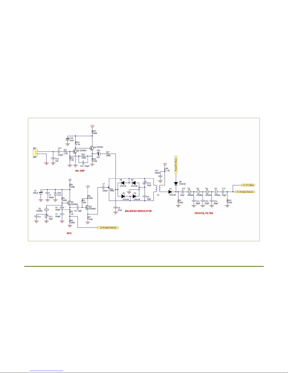
3.1 SSB generator..................................................................................................................................................6
3.2 Transmit mixer...............................................................................................................................................6
3.3 Power amplifier .............................................................................................................................................7
3.4 Receive mixer..................................................................................................................................................7
3.5 Receive audio..................................................................................................................................................8
4Parts List.................................................................................................................................................................. 14
4.1 Main Board Parts........................................................................................................................................ 14
4.2 Band Specific Parts .................................................................................................................................... 16
4.3 Off Board Parts............................................................................................................................................ 16
5Construction........................................................................................................................................................... 17
5.1 General............................................................................................................................................................ 17
5.2 Construction Steps..................................................................................................................................... 17
6Enclosure................................................................................................................................................................. 23
6.1 Rear Panel ..................................................................................................................................................... 23
6.2 Front Panel.................................................................................................................................................... 23
6.3 Mounting the PCB....................................................................................................................................... 23
6.4 Front panel label......................................................................................................................................... 24
6.5 Fitting the DDS VFO................................................................................................................................... 26
7Wiring up................................................................................................................................................................. 27
8Testing and alignment ....................................................................................................................................... 29
8.1 General............................................................................................................................................................ 29
8.2 Power on........................................................................................................................................................ 29
8.3 Receive............................................................................................................................................................ 30
8.4 Transmit......................................................................................................................................................... 30
8.5 Carrier frequency adjustment............................................................................................................... 32
9Operation................................................................................................................................................................. 33

MST Construction Manual –Issue 1 Page 3
List of Figures
Figure 1 MST Block diagram........................................................................................................................................5
Figure 2 SSB generator...................................................................................................................................................9
Figure 3 Transmit mixer............................................................................................................................................. 10
Figure 4 Power amplifier............................................................................................................................................ 11
Figure 5 Receive mixer................................................................................................................................................ 12
Figure 6 Receive audio................................................................................................................................................ 13
Figure 7 Component overlay .................................................................................................................................... 22
Figure 8 Front panel drilling guide........................................................................................................................ 25
Figure 9 DDS VFO front panel mounting ............................................................................................................. 26
Figure 10 Wiring diagram.......................................................................................................................................... 28
Figure 11 Typical circuit voltages........................................................................................................................... 31
Figure 12 Crystal filter response............................................................................................................................. 32

MST Construction Manual –Issue 1 Page 4
1INTRODUCTION
The MST (Minimalist Sideband Transceiver) is an easy to build and fun to use single sideband
QRP transceiver for the 40M or 80M amateur bands.
The MST transceiver follows a minimalist design making it inexpensive and simple to build yet
still delivering excellent performance and a pleasure to operate.
The MST PCB contains a complete SSB transceiver except for a VFO. You can add a VFO of your
own, as long as it has the correct frequency range and drive level, but to obtain best results it
should be used with the companion DDS VFO. The DDS VFO offers drift free performance and
features a clear backlit LCD display, selectable frequency steps and programmable IF offset.
MST Features:
1. Complete SSB transceiver on a single PCB (just add a VFO).
2. Superhet receiver using a 4 pole 10MHz crystal filter.
3. 5W PEP minimum power output using a rugged power MOSFET output stage.
4. Unwanted sideband suppression is typically 40dB.
5. All spurious transmit outputs below -45dBc.
6. AF and microphone gain controls.
7. Easy to adjust and set up.
8. Front panel LED transmit power and modulation indicator.
9. Plenty of audio output to drive a loudspeaker.
10. High quality double sided PCB with groundplane, solder mask and silk screen.
11. Simple and easy to build using all through hole components.
12. No complicated coil winding required. Uses inexpensive commercial coil assemblies for
tuned circuits.
A range of kits containing PCBs and hard to get parts for the MST and the DDS VFO are available
from www.ozQRP.com.

MST Construction Manual –Issue 1 Page 5
2BLOCK DIAGRAM
Figure 1 MST Block diagram
Receive Path
Transmit Path

MST Construction Manual –Issue 1 Page 6
3CIRCUIT DESCRIPTION
3.1 SSB GENERATOR
Transistor Q1 is configured as a Colpitts oscillator and acts as the 10MHz carrier oscillator in
transmit and beat frequency oscillator (BFO) in receive. The frequency of crystal X1 is set by
trimmer capacitor TC1 to a frequency slightly above the upper crystal frequency response. This
results in LSB being generated. Capacitor C1 is included in the PCB pattern but not used in this
application. The power supply to the oscillator is regulated with a 9.1V Zener diode ZD1.
The oscillator feeds buffer stage Q2 to provide a low impedance drive for the balanced
modulator. A lower level output of around 500mV pk-pk is obtained at the junction of Q1
emitter resistors to feed the receive product detector.
Transistors Q3 and Q4 are configured as a shunt feedback audio amplifier which has stable gain
and low output impedance. The low input impedance makes it ideally suited for low impedance
microphones. C16 is included to prevent RF feeding into the amplifier while C19 provides high
frequency roll off.
The balanced modulator is a diode switching type and doubly balanced. When the carrier signal
is positive diodes D1 and D4 conduct and when it is negative diodes D2 and D3 conduct. The
result is that no RF is present at the output transformer T1. If an audio signal is injected into the
bridge the balance is upset and a double sideband suppressed carrier signal is produced at the
output of T1. Note that capacitor C8 holds the junction of D1 and D2 at ground for RF.
Due to variations in component parameters the balance is not exact and so trimcap TC2 and
trimpot VR1 are adjusted to bring the modulator into balance. In practice up to 50dB of carrier
suppression can be achieved.
Diode D5 is used as an RF switch. With no DC current flowing the diode is a high impedance to
RF. In transmit around 6mA of DC current flows through D5 and it becomes a low impedance
path for RF. This feeds the output of the balanced modulator into the crystal filter. In receive D6
performs a similar function.
The crystal filter is a 10MHz 4 pole ladder type using closely matched crystals on the same
frequency. Capacitors C11 to C15 are selected to provide a usable 2.5KHz bandwidth. Resistors
R9 and R10 terminate the crystal filter in the correct resistance to give low ripple in the pass
band.
3.2 TRANSMIT MIXER
The transmit mixer is based around U5 a SA612 balanced mixer. The 10MHz LSB signal from the
crystal filter is fed single ended into pin1 while the other input on pin 2 is grounded to RF by
C65. The VFO signal of around 300mV pk-pk is fed into pin 6. The balanced output of the mixer
is fed to transformer T7 which is tuned to the difference of the VFO and carrier frequencies. The
transformer used here is actually a 10.7MHz IF transformer with an integral 47pF capacitor. An
external capacitor is added to lower the resonate frequency to match the transmit frequency.

MST Construction Manual –Issue 1 Page 7
A link coupled winding provides a low impedance output for the pre-driver built around
transistor Q9. The collector load is another IF transformer (T8) and resonated to the transmit
frequency in the same way as T7. In practice the two transformers form a 2 pole band pass filter
and adjusted to give the desired passband.
3.3 POWER AMPLIFIER
Transmit signal from the pre-driver is applied to the driver stage built around transistor Q6. A
BD139 works well here when biased with about 60mA of collector current. The design is well
proven using both shunt and series feedback to provide low input and output impedance and
good stable gain on the low HF bands.
The power amplifier is an IRF510 MOSFET and has been used in many designs. It is a good
candidate for the HF bands and easily provides over 5 Watts PEP of power from a 13.8 V drain
supply. The output from the driver is applied across resistor R38 and becomes the AC drive
component for Q7 gate. Zener diode ZD4 and trimpot VR2 provides a stable and variable DC
gate voltage to place Q7 just into conduction for linear service. There is a short ramp up of the
gate voltage when switching to transmit as capacitor C54 charges and is included to provide a
smooth gate voltage transition.
The drain load for Q7 is a broadband transformer T6. The turns ratio is chosen for best match
and to provide maximum output into a 50 ohm load. The waveform from Q7 can be high in
harmonics and so a 5 pole low pass filter is included to reduce the level of harmonic and other
spurious energy to an acceptable level. The values of the low pass filter components are band
dependant.
When the PTT is operated the transmit/receive relay is energized and the filtered transmit
signal is passed to the antenna. When the PTT is not operated the relay switches the antenna
through to the receive circuits. The relay also switches power to the transmit and receive
sections as required.
As a visual indication of power output and modulation, the transmit signal is sampled, rectified
and filtered by R39, D11 and C63. The resultant voltage is buffered by transistor Q8 to drive a
front panel LED via current limiting resistor R41.
The power supply is made available at an auxiliary connector and is intended to power a
companion VFO.
3.4 RECEIVE MIXER
Signals from the antenna are applied to a bandpass filter formed with two transformers T2, T3
and capacitors C21, C22 and C23. The antenna is link coupled to T2 while the output is fed from
a tap on the tuned primary winding of T3 to provide proper impedance matching.
The mixer U1 is another SA612. The input is protected with a pair of back to back diodes and fed
single ended into pin 1. Pin 2 is grounded to RF by C25. Zener diode ZD2 provides a stabilized
6.8 volt supply. VFO signal is injected into pin 6 at about 300mV pk-pk. The balanced output
which is a difference signal at approximately 10MHz is fed to broadband transformer T4. The
output of T4 is passed to the crystal filter when DC current flows through R19 and into D6.

MST Construction Manual –Issue 1 Page 8
3.5 RECEIVE AUDIO
The 10MHz SSB intermediate frequency (IF) signal from the crystal filter is applied to the
product detector U2. The product detector is formed with another SA612 and mixes the IF
signal with the 10MHz BFO signal to produce an audio output. The BFO is adjusted slightly
above the crystal filter upper response so that Lower Side Band signals are detected correctly.
A low noise balanced input audio amplifier is formed with U3 a NE5534. A reference supply for
the non-inverting input is obtained from the Zener diode stabilized supply for U2. The high
frequency response of U3 is limited by C35 and C42, while capacitors C37 and C36 reduce the
low frequency response.
The output of U3 is fed to a 1uF coupling capacitor and 1K resistor (R28) to the AF gain
potentiometer. When switching to transmit mode MOSFET Q5 is turned on rapidly through D9,
charging C45, and shorting the audio line to ground. When returning to receive mode Q5 slowly
turns off as C45 discharges via resistor R29. This circuit produces a very nice action eliminating
unwanted audio clicks and pops when switching between receive and transmit modes.
Audio from the AF gain control is amplified by U4, an LM386, to drive a loudspeaker. U4 is
configured for extra gain by including C41 and R26. C40 guards against RF entering the
amplifier input, while R30 and C47 help stabilize the output.

MST Construction Manual –Issue 1 Page 9
Figure 2 SSB generator

MST Construction Manual –Issue 1 Page 10
Figure 3 Transmit mixer

MST Construction Manual –Issue 1 Page 11
Figure 4 Power amplifier

MST Construction Manual –Issue 1 Page 12
Figure 5 Receive mixer

MST Construction Manual –Issue 1 Page 13
Figure 6 Receive audio

MST Construction Manual –Issue 1 Page 14
4PARTS LIST
4.1 MAIN BOARD PARTS
Quantity
Comment
Designator
2
22pF 50V disc ceramic NPO
C6, C9
2
68pF 50V disc ceramic NPO
C12, C14
3
82pF 50V disc ceramic NPO
C11, C13, C15
7
100pF 50V disc ceramic NPO
C4, C5, C26, C29, C33, C64, C66
1
220pF 50V disc ceramic
C19
2
470pF 50V disc ceramic
C34, C42
2
1nF 50V disc ceramic
C16, C24
1
10nF 50V disc ceramic
C8
2
10nF 63V polyester MKT
C35, C40
1
47nF 63V polyester MKT
C47
3
100nF 63V polyester MKT
C36, C37, C38
22
100nF 50V monolithic ceramic
C3, C7, C10, C25, C27, C28, C30, C31, C49, C50,
C51, C52, C53, C55, C56, C58, C63, C65, C67,
C69, C70, C72
1
220nF 63V polyester MKT
C17
4
1uF 16V RB electrolytic
C20, C43, C44, C45
2
10uF 16V RB electrolytic
C18, C41
1
22uF 16V RB electrolytic
C54
3
100uF 25V RB electrolytic
C2, C32, C39
3
470uF 25V RB electrolytic
C46, C48, C57
2
50pF ceramic trimcap 0.2" pitch
TC1, TC2
-
See Text
C1
4
10R 1/4W 1% resistor
R27, R30, R34, R35
1
15R 1/4W 1% resistor
R36
1
56R 1/4W 1% resistor
R38
6
100R 1/4W 1% resistor
R4, R6, R15, R17, R24, R43
1
220R 1/4W 1% resistor
R2
6
330R 1/4W 1% resistor
R9, R10, R26, R31, R32, R41
7
470R 1/4W 1% resistor
R7, R16, R18, R20, R37, R42, R46
3
1K 1/4W 1% resistor
R3, R28, R39
1
1.2K 1/4W 1% resistor
R33
3
2.2K 1/4W 1% resistor
R8, R11, R19
4
4.7K 1/4W 1% resistor
R13, R22, R23, R45
1
22k 1/4W 1% resistor
R44
1
47K 1/4W 1% resistor
R12
1
56K 1/4W 1% resistor
R5
1
100K 1/4W 1% resistor
R1
4
220K 1/4W 1% resistor
R21, R25, R29, R40
1
330K 1/4W 1% resistor
R14

MST Construction Manual –Issue 1 Page 15
Quantity
Comment
Designator
1
500R vertical multi turn trimpot
VR1
1
20K horizontal trimpot
VR2
10
1N4148 signal diode
D1, D2, D3, D4, D5, D6, D7, D8, D9, D11
1
1N4004 1A power diode
D10
1
9.1V 0.5W Zener diode
ZD1
4
6.8V 0.5W Zener diode
ZD2, ZD3, ZD4, ZD5
6
2N3904 NPN transistor
Q1, Q2, Q3, Q4, Q8, Q9
1
2N7000 MOSFET
Q5
1
BD139 NPN transistor
Q6
1
IRF510 Power MOSFET
Q7
3
SA612 RF mixer amp
U1, U2, U5
1
NE5534 low noise op-amp
U3
1
LM386N-4 audio power amp
U4
5
10MHz HC49 crystal
X1, X2, X3, X4, X5
1
DPDT DIP relay 12V coil
K1
1
FT37-43 4 turns: 3 turns 0.5mm
T1
4
42IF123 10.7MHz IF
Transformer
T2, T3, T7, T8
1
FT37-43 10 turns: 3 turns
0.5mm
T4
1
FT37-43 8 turns bifilar 0.25mm
T5
1
BN-43-202
2 turns: 5 turns 0.5mm
T6
2
PCB pin 1mm
P1 (ANT), P2 (GND)
6
2 pin 2.54mm pitch header
SK1 (MIC), SK2 (SPKR), SK4 (PTT), SK5 (RF), SK6
(VFO), SK7 (AUX)
1
3 pin 2.54mm pitch header
SK3 (AF GAIN)
1
2 way term block 5.08mm pitch
TB1 (POWER)
2
15mm long 3mm dia heat
shrink
0.5mm enamelled copper wire
0.25mm enamelled copper wire

MST Construction Manual –Issue 1 Page 16
4.2 BAND SPECIFIC PARTS
Quantity
40M
80M
Designator
1
6.8pF 50V disc ceramic NPO
33pF 50V disc ceramic NPO
C22
4
56pF 50V disc ceramic NPO
390pF 50V disc ceramic
C21, C23,
C68, C71
4
470pF 100V monolithic
ceramic C0G
820pF 100V monolithic ceramic
C0G
C59, C60,
C61, C62
2
1.1uH T50-2 15 turns 0.5mm
2.2uH T50-2 21 turns 0.5mm
L1, L2
4.3 OFF BOARD PARTS
Quantity
Comment
1
Plastic instrument case. 200mm x 155mm x 65mm
with aluminium panels. www.altronics.com.au
H0480F or equivalent.
1
red binding post
1
black binding post
1
SO239 panel mount socket
3
knobs
2
10K log pot 16mm
1
5mm amber LED and bezel
1
microphone socket
1
front panel label
1
loudspeaker 8 ohm 67mm square or equivalent
4
4g x 6mm self tapping screws
8
3mm x 6mm screws
4
3mm x 10mm screws
4
3mm nuts
1
solder lug
4
12mm long 3mm threaded nylon spacer
4
10mm long 3mm threaded nylon spacer
4
3mm x 16mm countersink screws
8
2 pin 2.54mm pitch header plugs
1
3 pin 2.54mm pitch header plug
hookup wire

MST Construction Manual –Issue 1 Page 17
5CONSTRUCTION
5.1 GENERAL
The MST is a built on a high quality fiberglass PCB. The PCB is doubled sided with tracks on the
bottom side with the top side being a continuous ground plane. The holes are plated through
and so it is not necessary to solder both sides to make connections. To assist construction the
component overlay is screen printed on the top side and a solder mask is included to guard
against solder bridges.
The ground plane is substantial and can sink quite a bit of heat from low wattage soldering irons
so ensure you use a good quality iron that can sustain the power required. You may find that
sometimes solder doesn’t appear to flow through to the top side. This is not necessarily a
problem because the plated through holes make a connection to the top side automatically.
Another point to consider is that plated through holes consume more solder than non-plated
holes and makes it more difficult to remove components.
The lesson is to double check the values and orientation of components before
installation.
There isn’t a ‘best’ scheme for loading the components. If desired you can build sections at a
time and test them out, but it is not necessary and in any case some sections rely on others
before they will operate. The suggested procedure is to load the smaller components first and
then work upwards.
5.2 CONSTRUCTION STEPS
Refer to the parts list and Figure 7when installing the components.
Step 1: Resistors
Install and solder a few at a time. It is easier and less confusing to install a group with the same
value rather than to cover a section of the PCB with mixed values. If in any doubt about reading
resistor values measure them with a multimeter before soldering.
Pass the pigtails through from the top and bend out slightly underneath to hold them in place.
Turn the PCB over and press down slightly to make them rest against the surface and solder. Cut
off the excess pigtail with side cutters.
Step 2: Diodes
Note the positive or cathode end before installation. The small Zener diodes look like signal
diodes so make sure you don’t get them mixed up.
Step 3: Non-polarized capacitors
Note the various types used. Ceramic disc, ceramic monolithic and polyester MKT. These are
non-polarized and can go in either way.

MST Construction Manual –Issue 1 Page 18
Step 4: Trimmer capacitors and trimpots
The type specified for the trimmer capacitor is quite small and has one lead electrically
connected to the screwdriver adjustment slot. Use a multimeter to determine this pin and solder
to the hole in the PCB connected to the ground plane.
Note that the carrier balance trimpot is a multi-turn vertical mount while the bias trimpot is a
horizontal mount type.
Step 5: Transistors
The 2N3904 transistors and 2N7000 MOSFET are orientated to match the screen silk
component overlay. The BD139 is installed so that the metal side of the body faces inwards
towards the centre of the PCB. Leave the IRF510 power MOSFET installation till later.
Step 6: Integrated Circuits
All ICs are 8 pin DIP types and have either a dot above pin 1 or a notch at the top between pin 1
and pin 8. This is shown in the top view diagram below. Double check they are installed in the
correct orientation.
Step 7: Electrolytic capacitors
These are polarized and must go in the correct way. The component overlay has a ‘+’ mark to
indicate the positive lead.
Step 8: Connectors
There are a number of connectors fitted to the PCB to provide a neat finished product. They also
allow easy removal of the PCB if required. The 2.54mm pitch connectors have a vertical
polarizing piece and the connectors are installed with this piece towards the centre of the PCB.
The power connector is a 2 way terminal block and the terminal openings face towards the edge
of the PCB.
The antenna and its ground connection are soldered to a pair of 1mm PCB pins. This is done to
ensure a positive low resistance connection.
Step 9: IF transformers and relay
The four IF transformers can only go in one way and so are simply fitted into the holes in the
PCB and soldered. The relay is inserted into the board and soldered.
1
2
3
4
8
7
6
5

MST Construction Manual –Issue 1 Page 19
Step 10: Coils
Output transformer T6
T6 is wound on a 13mm two hole
ferrite balun former type BN-43-202.
The edges of the holes are quite sharp
and can scrape the enamel off the
wires. To reduce scraping and the risk
of shorts, cut two lengths of 3mm heat
shrink and feed into the balun former
holes.
Wind the 2 turn primary with 0.5mm
enamelled copper wire. The primary
winding connects to Q7 drain. A turn is
where the wire passes up through one
hole and down the other.
Starting at the opposite end wind the 5
turn secondary in the same manner.
Use 0.5mm enamelled copper wire.
The secondary is the output and
connects to the LPF.
Scrape the enamel off the ends of the
wires and tin with solder. Check with a
multimeter that there are no shorts
between the windings before installing
in the PCB.
Low Pass Filter Coils L1 and L2
Wind the turns shown below for the required
band using 0.5mm enamelled copper wire on a
T50-2 toroid.
40M: 15 turns. 80M: 21 turns
Note the direction of winding as this makes for
a neater alignment of the toroid in the PCB.
Scrape the enamel off the ends of the wires
and tin with solder before installing in the
PCB.

MST Construction Manual –Issue 1 Page 20
Transformers T1 and T4
Use a FT37-43 ferrite toroid and 0.5mm
enamelled copper wire.
T1: 4 turn primary (balanced modulator), 3
turn secondary (output)
T4: 10 turn primary (U1), 3 turn secondary
(output)
Scrape the enamel off the ends of the wires
and tin with solder before installing in the
PCB.
Bifilar transformer T5
Use a FT37-43 ferrite toroid and 0.25mm
enamelled copper wire.
Take two 300mm lengths lay them parallel
and then twist together until there are about 3
twists per centimetre. A vice and battery drill
with a hook shaped bit make this job easy.
Wind on 8 turns. Scrape some enamel off the
ends and use a multimeter to find the start and
end of each winding.
Take the start of one winding and the end of
the other winding and twist together to form
the centre tap.
Trim the leads with sidecutters and tin with
solder before installing. Push the wires
through the holes in the PCB and sit the toroid
so that it rests against the surface of the board.
Ensure the two-wire centre tap goes to the
middle hole in the PCB overlay for T5.
Table of contents
Other ozQRP Transceiver manuals