Panasonic KX-TG4011LAT User manual

© Panasonic System Networks Co., Ltd. 2010
Unauthorized copying and distribution is a violation
of law.
ORDER NO. KM41006120CE
Telephone Equipment
Model No. KX-TG4011LAT
KX-TG4012LAT
KX-TG4013LAT
KX-TGA403LAT
Expandable Digital Cordless Phone
T: Black Metallic Version
(for Latin America)

2
KX-TG4011LAT/KX-TG4012LAT/KX-TG4013LAT/KX-TGA403LAT

3
KX-TG4011LAT/KX-TG4012LAT/KX-TG4013LAT/KX-TGA403LAT
TABLE OF CONTENTS
PAGE PAGE
1 Safety Precautions----------------------------------------------- 4
1.1. For Service Technicians --------------------------------- 4
2 Warning -------------------------------------------------------------- 4
2.1. Battery Caution--------------------------------------------- 4
2.2. About Lead Free Solder (PbF: Pb free)-------------- 4
2.3. Discarding of P. C. Board-------------------------------- 5
3 Specifications ----------------------------------------------------- 6
4 Technical Descriptions ----------------------------------------- 7
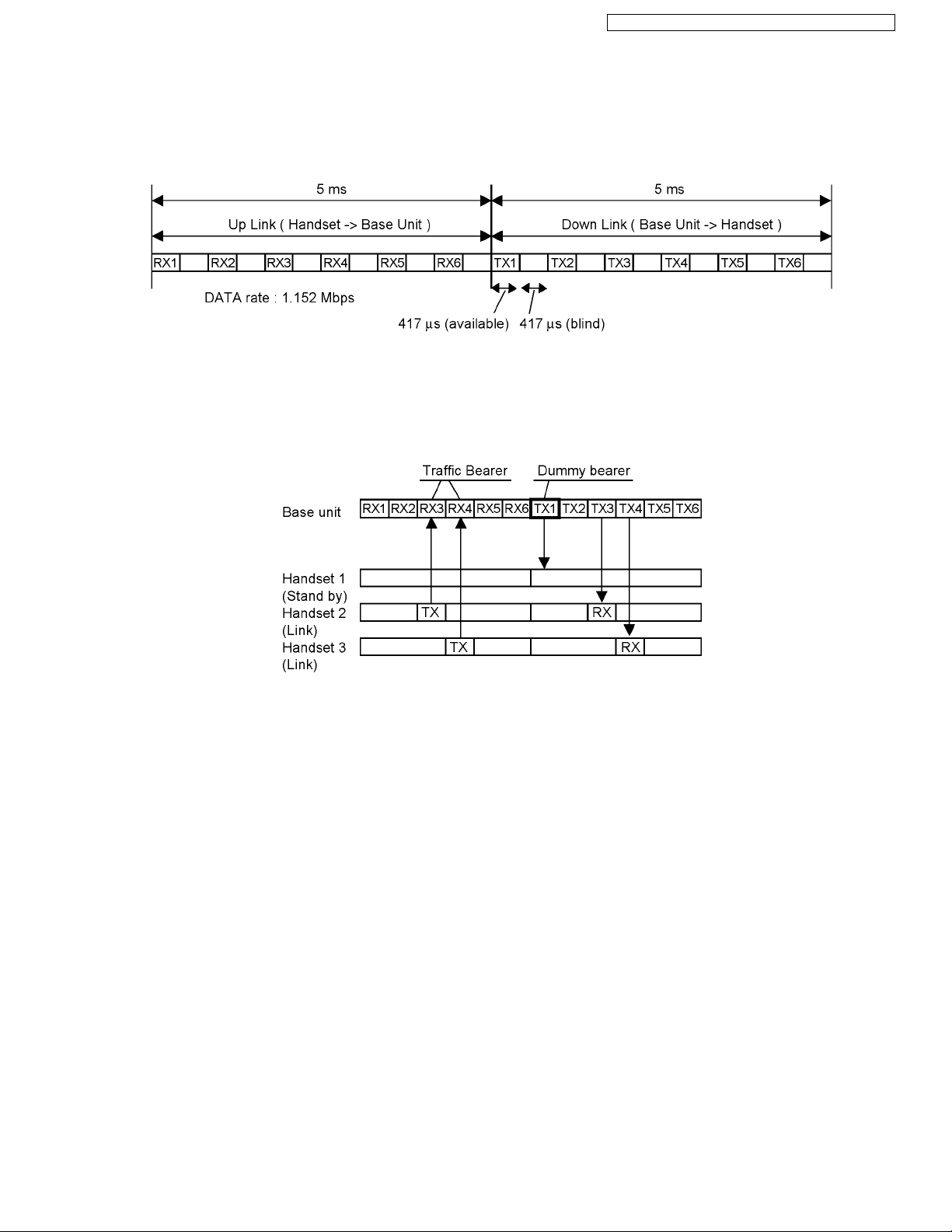
4.1. US-DECT Description ------------------------------------ 7
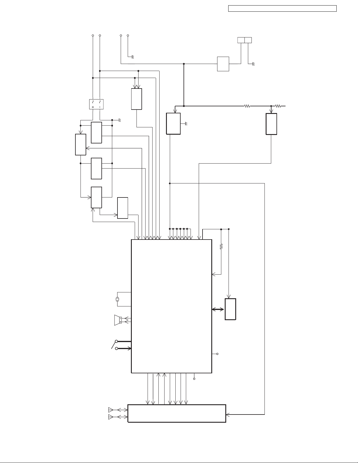
4.2. Block Diagram (Base Unit_Main)---------------------- 9
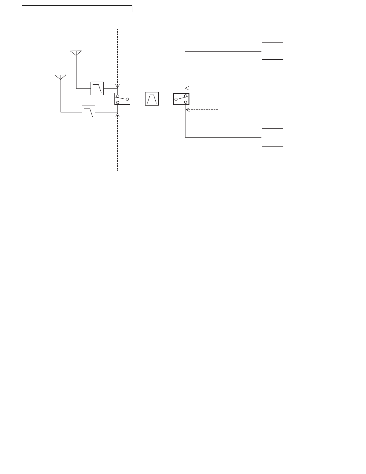
4.3. Block Diagram (Base Unit_RF Part) -----------------10
4.4. Circuit Operation (Base Unit) -------------------------- 11
4.5. Block Diagram (Handset)-------------------------------18
4.6. Block Diagram (Handset_RF Part)-------------------19
4.7. Circuit Operation (Handset)----------------------------20
4.8. Circuit Operation (Charger Unit) ----------------------22
4.9. Signal Route -----------------------------------------------23
5 Location of Controls and Components ------------------24
6 Installation Instructions ---------------------------------------24
7 Operating Instructions-----------------------------------------24
8 Test Mode ----------------------------------------------------------25
8.1. Engineering Mode ----------------------------------------25
9 Service Mode -----------------------------------------------------29
9.1. How to Clear User Setting (Handset Only)---------29
10 Troubleshooting Guide ----------------------------------------30
10.1. Troubleshooting Flowchart -----------------------------30
11 Disassembly and Assembly Instructions ---------------41
11.1. Disassembly Instructions -------------------------------41
11.2. How to Replace the Handset LCD -------------------44
12 Measurements and Adjustments---------------------------45
12.1. Equipment Required -------------------------------------45
12.2. The Setting Method of JIG -----------------------------45
12.3. Adjustment Standard (Base Unit)---------------------48
12.4. Adjustment Standard (Charger Unit)-----------------49
12.5. Adjustment Standard (Handset) ----------------------50
12.6. Things to Do after Replacing IC or X'tal ------------51
12.7. Frequency Table ------------------------------------------53
13 Miscellaneous ----------------------------------------------------54
13.1. How to Replace the Flat Package IC----------------54
13.2. How to Replace the Shield Case ---------------------56
13.3. How to Replace the LLP (Leadless Leadframe
Package) IC------------------------------------------------58
13.4. Terminal Guide of the ICs, Transistors and
Diodes -------------------------------------------------------60
14 Schematic Diagram ---------------------------------------------61
14.1. For Schematic Diagram---------------------------------61
14.2. Schematic Diagram (Base Unit_Main) --------------62
14.3. Schematic Diagram (Handset_Main) ----------------64
14.4. Schematic Diagram (Charger Unit) -----------------66
15 Printed Circuit Board-------------------------------------------67
15.1. Circuit Board (Base Unit_Main)-----------------------67
15.2. Circuit Board (Handset_Main)-------------------------69
15.3. Circuit Board (Charger Unit) ---------------------------71
16 Exploded View and Replacement Parts List -----------72
16.1. Cabinet and Electrical Parts (Base Unit) -----------72
16.2. Cabinet and Electrical Parts (Handset) -------------73
16.3. Cabinet and Electrical Parts (Charger Unit) -------74
16.4. Accessories ------------------------------------------------75
16.5. Replacement Parts List--------------------------------- 76

4
KX-TG4011LAT/KX-TG4012LAT/KX-TG4013LAT/KX-TGA403LAT
1 Safety Precautions
1.1. For Service Technicians
•Repair service shall be provided in accordance with repair technology information such as service manual so as to
prevent fires, injury or electric shock, which can be caused by improper repair work.
1. When repair services are provided, neither the products nor their parts or members shall be remodeled.
2. If a lead wire assembly is supplied as a repair part, the lead wire assembly shall be replaced.
3. FASTON terminals shall be plugged straight in and unplugged straight out.
•ICs and LSIs are vulnerable to static electricity.
When repairing, the following precautions will help prevent recurring malfunctions.
1. Cover plastic parts boxes with aluminum foil.
2. Ground the soldering irons.
3. Use a conductive mat on worktable.
4. Do not grasp IC or LSI pins with bare fingers.
2Warning
2.1. Battery Caution
1. Danger of explosion if battery is incorrectly replaced.
2. Replace only with the same or equivalent type recommended by the manufacturer.
3. Dispose of used batteries according to the manufacturer’s Instructions.
2.2. About Lead Free Solder (PbF: Pb free)
Note:
In the information below, Pb, the symbol for lead in the periodic table of elements, will refer to standard solder or solder that
contains lead.
We will use PbF solder when discussing the lead free solder used in our manufacturing process which is made from Tin (Sn),
Silver (Ag), and Copper (Cu).
This model, and others like it, manufactured using lead free solder will have PbF stamped on the PCB. For service and repair
work we suggest using the same type of solder.
Caution
• PbF solder has a melting point that is 50 °F ~ 70 °F (30 °C ~ 40 °C) higher than Pb solder. Please use a soldering iron with
temperature control and adjust it to 700 °F ± 20 °F (370 °C ± 10 °C).
• Exercise care while using higher temperature soldering irons.:
Do not heat the PCB for too long time in order to prevent solder splash or damage to the PCB.
• PbF solder will tend to splash if it is heated much higher than its melting point, approximately 1100 °F (600 °C).
• When applying PbF solder to double layered boards, please check the component side for excess which may flow onto the
opposite side (See the figure below).

5
KX-TG4011LAT/KX-TG4012LAT/KX-TG4013LAT/KX-TGA403LAT
2.2.1. Suggested PbF Solder
There are several types of PbF solder available commercially. While this product is manufactured using Tin, Silver, and Copper
(Sn+Ag+Cu), you can also use Tin and Copper (Sn+Cu), or Tin, Zinc, and Bismuth (Sn+Zn+Bi). Please check the
manufacturer's specific instructions for the melting points of their products and any precautions for using their product with other
materials.
The following lead free (PbF) solder wire sizes are recommended for service of this product: 0.3 mm, 0.6 mm and 1.0 mm.
2.3. Discarding of P. C. Board
When discarding P. C. Board, delete all personal information such as telephone directory and caller list or scrap P. C. Board.

6
KX-TG4011LAT/KX-TG4012LAT/KX-TG4013LAT/KX-TGA403LAT
3 Specifications
Note:
• Design and specifications are subject to change without notice.
Note for Service:
•Operation range: Up to 300 m outdoors, Up to 50 m indoors, depending on the condition.
•Analog telephone connection: Telephone Line

7
KX-TG4011LAT/KX-TG4012LAT/KX-TG4013LAT/KX-TGA403LAT
4 Technical Descriptions
4.1. US-DECT Description
The frequency range of 1.91 GHz-1.93 GHz is used. Transmitting and receiving carrier between base unit and handset is same
frequency. Refer to Frequency Table (P.53).
4.1.1. TDD Frame Format
4.1.2. TDMA system
This system is the cycles of 10 ms, and has 6 duplex paths, but maximum duplex communication path is 5 because of dummy
bearer use.
In 1 slot 417 µs, the 10 ms of voice data is transmitted.
•2 - Handsets Link
Traffic Bearer
A link is established between base unit and handset.
The state where duplex communication is performed.
Handset doesn't make up duplex in no free RF channels because of interference. (*1)
Dummy Bearer
Base unit sends Dummy-data to the all stand-by state handsets.
Handsets receive that data for synchronization and monitoring request from the base unit.
Base unit doesn't send Dummy bearer in no free RF channels because of interference. (*1)
Note:
(*1) It is a feature under FCC 15 regulation and for interference avoidance.
In the case of checking RF parts, it is better in least interference condition.

8
KX-TG4011LAT/KX-TG4012LAT/KX-TG4013LAT/KX-TGA403LAT
4.1.3. Signal Flowchart in the Radio Parts
Reception
A voice signal from TEL line is encoded to digital data "TXDATA" by BBIC (IC501) in a base unit.
Then TXDATA goes to RF PART and it's modulated to 1.9 GHz. The RF signal is amplified and fed to a selected antenna.
As for a handset RF, RF signal is received in one antenna.
BBIC down-converts to 864 kHz IF signal from RX signal and demodulates it to digital data "RXDATA".
BBIC (IC1) converts RXDATA into a voice signal and outputs it to speaker.
Transmission
A voice signal from microphone is encoded to digital data "TXDATA" by BBIC (IC1) in a handset.
Then TXDATA goes to RF PART, and it's modulated to 1.9 GHz. The RF signal is amplified and fed to a antenna.
As for a base unit RF, RF signal is received in two antennas.
BBIC (IC501) compares RF signal levels and selects the antenna to be used. Then BBIC down-converts to 864 kHz IF signal
from RX signal in the selected antenna, and demodulates it to digital data "RXDATA".
BBIC (IC501) converts RXDATA into a voice signal and outputs it to TEL line.

9
KX-TG4011LAT/KX-TG4012LAT/KX-TG4013LAT/KX-TGA403LAT
4.2. Block Diagram (Base Unit_Main)
SW1
ٌ
KX-TG4011/4012/4013 BLOCK DIAGRAM (Base Unit_Main)
D101
CHARGE_CONTAC
T
+
-
SP
X501
13.824 MHz
ANT2ANT1
TEL JACK
L1T
L1R
DCP
DCM
DC JACK
RLY
SIDE TONE
CIRCUIT
Q161
Q141
BELL
DETECT
HOOK
BELL
Q111
LIN
LOUT
RF_PART
HSMIP
HSMIN
IC501
BBIC
INUSE
DETECT 2
INUSE
DETECT 1
RECEIVE
AMP
DCIN 1
DCIN 2
IC302
VCCPA
VBAT_APU
VBAT
VCC_FE
VCC_IF
VCC_VCO
PDN DET
3.0V
DOUBOUT
SCL, SDA
WP
IC611
EEPROM
MEMORY
R151,R152 R131, R133
Q171
VBAT
KEY 1
KEY C
SPOUTN
SPOUTP
3.0 V
REGULATOR
IC331
RESET IC
STM/CKM
R371
R372
VCCA
VCC
ANT2
ANT1
RXp
RXn
RXON
TXp
TXn
TXON
RESET
RSTN

10
KX-TG4011LAT/KX-TG4012LAT/KX-TG4013LAT/KX-TGA403LAT
4.3. Block Diagram (Base Unit_RF Part)
KX-TG4011/4012/4013 BLOCK DIAGRAM (Base Unit_RF Part)
DA801
ANT2
ANT1
TXON
RXON
RXp
RXn
ANT2
ANT1
TXp
TXn

11
KX-TG4011LAT/KX-TG4012LAT/KX-TG4013LAT/KX-TGA403LAT
4.4. Circuit Operation (Base Unit)
General Description:
(BBIC, EERROM) is a digital speech/signal processing system that implements all the functions of speech compression and
memory management required in a digital telephone.
The BBIC system is fully controlled by a host processor. The host processor provides activation and control of all that functions
as follows.
4.4.1. BBIC (Base Band IC: IC501)
•DTMF Generator
When the DTMF data from the handset is received, the DTMF signal is output.
•Caller ID demodulation
The BBIC implements monitor and demodulate the FSK/DTMF signals that provide CID information from the Central Office.
•Digital Switching
The voice signal from telephone line is transmitted to the handset or the voice signal from the handset is transmitted to the
Telephone line, etc. They are determined by the signal path route operation of voice signal.
•Block Interface Circuit
RF part, Key scan, Telephone line.
4.4.2. EEPROM (IC611)
Following information data is stored.
•Settings
ex: message numbers, ID code, Flash Time, Tone/Pulse

12
KX-TG4011LAT/KX-TG4012LAT/KX-TG4013LAT/KX-TGA403LAT
4.4.3. Power Supply Circuit/Reset Circuit
The power supply voltage from AC adaptor is converted to VBAT (3.0V) in IC302. And +3.0V for peripherals and analog part is
insulated from VBAT by Doubler of BBIC.
Circuit Operation:

13
KX-TG4011LAT/KX-TG4012LAT/KX-TG4013LAT/KX-TGA403LAT
4.4.3.1. Charge Circuit
The voltage from the AC adaptor is supplied to the charge circuits.

14
KX-TG4011LAT/KX-TG4012LAT/KX-TG4013LAT/KX-TGA403LAT
4.4.4. Telephone Line Interface
Telephone Line Interface Circuit:
Function
• Bell signal detection
• ON/OFF hook and pulse dial circuit
• Side tone circuit
Bell signal detection and OFF HOOK circuit:
In the idle mode, Q141 is open to cut the DC loop current and decrease the ring load. When ring voltage appears at the Tip (T)
and Ring (R) leads (When the telephone rings), the AC ring voltage is transferred as follows:
T →L101 →R111 →C111 →Q111 →BBIC pin 5 [BELL]
When the CPU (BBIC) detects a ring signal, Q141 turns on, thus providing an off-hook condition (active DC current flow through
the circuit). Following signal flow is the DC current flow.
T →L101 →D101 →Q141 →Q161 →R163 →R167 →D101 →L102 →P101 →R
ON HOOK Circuit:
Q141 is open, Q141 is connected as to cut the DC loop current and to cut the voice signal. The unit is consequently in an on-
hook condition.
Pulse Dial Circuit:
Pin 6 of BBIC turns Q141 ON/OFF to make the pulse dialing.
Side Tone Circuit:
Basically this circuit prevents the TX signal from feeding back to RX signal. As for this unit, TX signal feed back from Q161 is
canceled by the canceller circuit of BBIC.

15
KX-TG4011LAT/KX-TG4012LAT/KX-TG4013LAT/KX-TGA403LAT
4.4.5. Parallel Connection Detect Circuit/Auto Disconnect Circuit
Function:
In order to disable call waiting and stutter tone functions when using telephones connected in parallel, it is necessary to have a
circuit that judges whether a telephone connected in parallel is in use or not. This circuit determines whether the telephone
connected in parallel is on hook or off hook by detecting changes in the T/R voltage.
Circuit Operation:
Parallel connection detection when on hook:
When on hook, the voltage is monitored at pin 17 of IC501. There is no parallel connection if the voltage is
0.54 V or higher, while a parallel connection is deemed to exist if the voltage is lower.
Parallel connection detection when off hook:
When off hook, the voltage is monitored at pin 18 of IC501; the presence/absence of a parallel connection is determined by
detecting the voltage changes.
If the Auto disconnect function is ON and statuses are Hold, BBIC disconnects the line after detecting parallel connection is off
hook.

16
KX-TG4011LAT/KX-TG4012LAT/KX-TG4013LAT/KX-TGA403LAT
4.4.6. Calling Line Identification (Caller ID)
Function:
Caller ID
The caller ID is a chargeable ID which the user of a telephone circuit obtains by entering a contract with the telephone company
to utilize a caller ID service. For this reason, the operation of this circuit assumes that a caller ID service contract has been
entered for the circuit being used. The data for the caller ID from the telephone exchange is sent during the interval between the
first and second rings of the bell signal. The data from the telephone exchange is a modem signal which is modulated in an FSK
(Frequency Shift Keying) * format. Data "1"is a 1200 Hz sine wave, and data "0"is a 2200 Hz sine wave. There are two types of
the message format which can be received: i.e. the single message format and plural message format. The plural message
format allows to transmit the name and data code information in addition to the time and telephone number data.
*: Also the telephone exchange service provides other formats.

17
KX-TG4011LAT/KX-TG4012LAT/KX-TG4013LAT/KX-TGA403LAT
Call Waiting Caller ID
Calling Identity Delivery on Call Waiting (CIDCW) is a CLASS service that allows a customer, while off-hook on an existing call,
to receive information about a calling party on a waited call. The transmission of the calling information takes place almost
immediately after the customer is alerted to the new call so he/she can use this information to decide whether to take the new
call.
Function:
The telephone exchange transmits or receives CAS and ACK signals through each voice RX/TX route. Then FSK data and
MARK data pass the following route.
Telephone Line →P101 →L101, L102 →C121, C122 →R121, R122 →IC501 (25, 24).
If the unit deems that a telephone connected in parallel is in use, ACK is not returned even if CAS is received, and the
information for the second and subsequent callers is not displayed on the portable handset display.

18
KX-TG4011LAT/KX-TG4012LAT/KX-TG4013LAT/KX-TGA403LAT
4.5. Block Diagram (Handset)
IC1
IC3
MICp
AVD
LD0_CTRL
MICn
LSRp
LSRn
BELL_LED
PAOUTp
PAOUTn
CKM//STM
CKM/STM
BBIC
RESET
CHG_CTL
CHG_DET
WP, CLK, DATA
P3_3~P3_7
P1_1~P1_4
CHARGE Q4 D7
MIC
Receiver
LED
3V
Monitor SP
LCD KEYS
IC801
RF PART
ANT1
X1
10.368 MHz
EEPROM
3V
BATTERY
(BELL)
BATTERY
3V
BATTERY
3V
KX-TGA403 BLOCK DIAGRAM (Handset)
KEY_LED
Q7
LED
(KEY)
TXn
Power_adj
TXp
VDD_PADRV
PSEL
PON
TXON
RXON
RF_RXn
RF_RXp
CP_VOUT2
BATTERY
VDDPA
1.8V
VDD2
VDD1
3V
Q2
1.8V
C144
D1

19
KX-TG4011LAT/KX-TG4012LAT/KX-TG4013LAT/KX-TGA403LAT
4.6. Block Diagram (Handset_RF Part)
KX-TGA403 BLOCK DIAGRAM (Handset_RF Part)
DA801
TXON
RXON
ANT
RF_RXn
RF_RXp

20
KX-TG4011LAT/KX-TG4012LAT/KX-TG4013LAT/KX-TGA403LAT
4.7. Circuit Operation (Handset)
4.7.1. Outline
Handset consists of the following ICs as shown in Block Diagram (Handset) (P.18).
• DECT BBIC (Base Band IC): IC1
- All data signals (forming/analyzing ACK or CMD signal)
- All interfaces (ex: Key, Detector Circuit, Charge, DC/DC Converter, EEPROM, LCD, RF Power Amp.)
- PLL Oscillator
-Detector
- Compress/Expander
- Reception
• RF Power Amp: IC801
- Amplifier for transmission
• EEPROM: IC3
- Temporary operating parameters (for RF, etc.)
4.7.2. Power Supply Circuit/Reset Circuit
Circuit Operation:
When power on the Handset, the voltage is as follows;
BATTERY(2.2 V ~ 2.6 V: BATT+) →F1 →Q2 (1.8 V), IC1-43pin (2.5V)
The Reset signal generates IC1 (61 pin) and 1.8 V.
This manual suits for next models
3
Table of contents
Other Panasonic Digital Cordless Phone manuals