manuals.online logo
Brands
  1. Home
  2. •
  3. Brands
  4. •
  5. Pioneer
  6. •
  7. Speakers
  8. •
  9. Pioneer CX-683 User manual

Pioneer CX-683 User manual

PIONEER CORPORATION 4-1, Meguro 1-Chome, Meguro-ku, Tokyo 153-8654, Japan
PIONEER ELECTRONICS SERVICE INC. P.O.Box 1760, Long Beach, CA 90801-1760 U.S.A.
PIONEER EUROPE N.V. Haven 1087 Keetberglaan 1, 9120 Melsele, Belgium
PIONEER ELECTRONICS ASIACENTRE PTE.LTD. 253 Alexandra Road, #04-01, Singapore 159936
C PIONEER CORPORATION 2000 K-FZU. JAN. 2000 Printed in Japan
ORDER NO.
CRT2441
MD MECHANISM MODULE
CX-683
Service
Manual
NOTE:
-This Service Manual describes the operations of the MD mechanism module being used for the models
listed in the Table indicated below.
-Be sure to reference this service manual as well as the service manual prepared for respective models
must be referenced before implementing the repair work.
CONTENTS
1. CIRCUIT DESCRIPTIONS...........................................2
2. MECHANISM DESCRIPTIONS.................................12
3. DISASSEMBLY .........................................................15
MODEL SERVICE MANUAL MD MECHANISM MODULE
MEH-P5100R/EW CRT2445 CXK3110
1. CIRCUIT DESCRIPTIONS
1.1 RF AMPLIFIER BLOCK (CXA2523AR : IC101)
This section works to process the output signals from the MD pickup to generate signals to be transferred to the next
stage, namely, the DSP section (IC201).
Respective photo-detector output signals A, B, C, D, E and F are I-V converted and processed inside the RF amplifier to
become FE, TE and ADIP signals.
Also, I and J outputs which have been I-V converted by the amplifier incorporating the photo-detector inside the
pickup are processed to become the RF signals and the PEAK and BOTM signals.
Meanwhile, since this system is of the single power (+3.3V) specification, the reference voltage for the servo-signals is
Vc (1.65V).
Vc is being output from this RF amplifier (IC101, 3pin).
(Note) Do not short the Vc and GND while making measurements.
2
CX-683
Fig. 1 : CXA2523AR BLOCK DIAGRAM
3
CX-683
2) RF Amplifier
I and J signals being I-J converted in the pickup are entered to 1 and 2 pins. Then, their difference signal (group
signal) and sum signal (bit signal) are generated on RFA1 and RFA2, respectively.
RFA2 and RFA3 are switching operational amplifiers. The amplifiers detect high reflection (Premastered) and low
reflection (Recordable) using the disc detector switch (S404) to switch to the gain selected by the serial command
HLPT or PTGR.
RF signal (46 pin) is operated and conducted to the AGC circuit and equalizer via C122 to generate RF signal (36 pin).
RF signal is maintained essentially at a constant level (approximately at 1.1 Vpp) by the AGC circuit.
This signal is entered to the signal processing LSI (IC201: 55 pins) for the data processing as well as control of the
Premastered Disc playing spindle.
1) APC (Automatic Power Control) Circuit
Since laser diode (LD) has temperature characteristics, the APC circuit is provided to control current flow using the
monitor diode so that the output may be kept at a constant level.
LD current is determined by measuring voltage across V1 and 3VD.
The current value should be approximately 40 mA (0.4V/10Ω).
19
20 6
10
12 11
–
+
21
12 14
13
VREF
Q102
UMD2N
LDCNT
R103 PD
APC REF
CXA2523AR
MON Vr
MD LD
3VD C105 R1
LD+
3VD
R102 0R0
R101 10
VI
100/6R3
R108
APC
C108 R001
R109 470K
R110
6R8K
1.25V
6R8K
C106 +
GNDVR
R104
0ΩLD –
PU unit
47K
C107
3VP 22P
1
238
–
+
–2
–1
–1
–2
–1 –2
–1
–1
–1
–2
–2
48 47
22
20
22
46 40 39
25
20
36
37
Peak/Bottom
Hold
BPF
fo=720kHz Peak
Hold
BPF3T PEAK3T
PBH1
J
MORFO MORFI RFO
IRFA1
OFST
ABCD
RFA3
PEAK
BOTM
F0CNT
WBLADJ
PBSW
GRVA
HLPT
GRV
RFA2
PTGR
AGC EQA
3TADJ
F0CNT
I3
EQADJ
RFAGC
<To IC201>
RF
C122
R022
C124
R047
4
CX-683
3) I-V, ADIP, ABCD and FE Amplifier Blocks
They are used for I-V conversion of photo-detector signals (A to F pins) from the pickup.
ADIP, FE and full quantity of light signals are generated from A to D signals, and TE signal is generated from E and F
signals.
The ABCD amplifier generates the full quantity of light signal for the main spot. This signal is sum of A to D signals
after I-V conversion. According to the level of the full quantity of light signal, resistance value of I-V is automatically
adjusted so that ADIP, FE and TE signals may be maintained at the specified level.
FE and TE signals output from both the Recordable and Premastered Discs are adjusted to approximately 1 Vpp and
1.7 Vpp, respectively. This adjustment is executed whenever a disc is inserted.
ABCD signal entered to the signal processing LSI (IC201: 64 pins) is also used for generating FOK and defect detect
signals.
The ADIP amplifier is used for generating ADIP signal that is present only on the Recordable Disc.
Addresses are already recorded on the Recordable Disc by wobbling FM signal that uses 22.05 KHz as the carrier. In
order to detect wobble elements, noise elements of the signal are eliminated on the BPF, then the signal is output to
the ADFM via the AGC. The signal is then sent to C111 for DC cut and binary converted on the comparator to generate
ADFG signal. ADFG signal is entered to the signal processing LSI (IC201: 78 pins) to control the address and spindle
when the Recordable Disc is played.
–
–
+
+
4+
–
5+
–
6+
–
7
25
+
–
–
–
+
+
–
–
–
–35 64
34
29
30
32
65
78
20
43 31
Focus err amplifier
IVR0-IVR4
FE R219
100
AIV
AAA BB
CC
AA
DD
AA
CC
BB
DD
AA
BB
CC
DD
IVR0-IVR4
BIV
B
ABCD
BB
IVR0-IVR4
CIV
CCC
IVR0-IVR4
DIV
ABCDA
FEA
ATA
DDD
ADAGC
ADFM
ADIN
WBLADI F0CNT
ADFG
ADDC
C11
4700P
<To IC201 pins>
BPF
fo=22.05kHz
BPF22
ADIPAGC
<To IC201 pins>
<To IC201 pins>
AGC
BPFC
COMP
ABCD amplifier
I-V amplifier ADIP amplifier
5
CX-683
4) TE and SE Amplifiers
Side spot E and F signals are I-V converted, then entered to the EF balance adjusting amplifier. Then, after polarity of
the tracking error signal is switched by the TE differential amplifier (TESW), the signal is conducted to the gain
amplifier to generate TE signal.
Select PTGR = 1 for the Pit play and PTGR = 2 for the group play.
The EF balance adjusting amplifier automatically adjusts an EF balance resistance value so that level of SE signal
becomes the same as the reference voltage Vc when the TRKG made is open.
The SE amplifier generates TE signal from the LPF, then enters it into the signal processing LSI (IC201: 73 pins) for
digital equalizing.
Condition PTGR HLPT
PremasterdDisc Pit High reflection 1 2
RecordableDisc Pit Low reflection 1 1
Groove Low reflection 2 1
–1
+1
+2
–2
8+
–
9+
–26
27
–2
–1 74
28
–2
–1 73
IVR0-IVR4 EFB0-EFB4
EIV
EEE
EE
FF
IVR0-IVR4
FIV
FFF
CSLED
TG
TEA
TESW
PTGR
TE <To IC201 pins>
R221
SEA
SE <To IC201 pins>
R220
100
100
C110
R068
Pit / GR Select
Pit
GR
1.2 SIGNAL PROCESSOR BLOCK (CXD2655BR IC201)
1.2.1 SERVO BLOCK
1) Servo Block
This block offers servo control over the focus, tracking, spindle and carriage.
FE, TE and SE signals from the amplifier are A/D converted, equalized on D.F (digital filer) block, and then output to
PWM.
The spindle servo detects phase and frequency of input signal (from 55 pin RFI terminal for Pre_disc and 78 pin ADFG
terminal for Rec_disc), then outputs it to PWM via the filter.
These signals are power amplified on the driver IC401 to drive the actuator and motor.
Focus Servo System
In order to close the focus, the actuator is driven up near to the Disc once, then moved down.
As soon as up-move is started, the spindle is kicked for 252 ms, then ofst drive is turned on.
Focus close is carried out when the following conditions are met:
1) The actuator, after having approached the Disc once, is now moving away from it.
2) FOK = H (Can be monitored on the mnt0 terminal when the mnt selector is set to 00.)
3) FZC =
↑
After the focus close has been started, the microcomputer judges the operation is complete if FOK = H continues for 32 ms.
6
CX-683
A/DFE
FIN (For monitoring control signal)
FOP
FOM
A, B, C, D
RF
amplifier
Driver
Pick up
IC201IC101
IC401
BIAS
EQ PWM FFDR 88pin
FRDR 89pin
close_point
Close operation is judged to have
successfully ended when FOK
remains at "H" for 32 ms.
FE
FOK
FZC
Tracking Servo System
The system causes the microcomputer to issue the tracking close instruction to the IC, then switches the spindle
control from the ofst drive to the CLV control.
The close operation completes when the Disc address has been read after the spindle LOCK signal went high
(Can be monitored on the mnt0 terminal when the mnt selector is set to 00).
Carriage Servo System
The carriage operation is turned on at the moment when the tracking close instruction is issued. The system drives
the carriage according to DC_ofst volume specified on the actuator.
7
CX-683
A/DTE
TIN (For monitoring control signal)
TOP
TOM
E
F
RF
amplifier
Driver
Pick up
IC201IC101
IC401
OFST
EQ PWM TFDR 86pin
TRDR 85pin
A/DSE
CIN (For monitoring control signal)
COP
COM
E
F
RF
amplifier
Driver
Carriage Motor
Pick up
IC201IC101
IC401
OFST
EQ
Move
PWM SFDR 92pin
SRDR 91pin
M
Timing Control
Timing Control
RF
ADFG
SIN (For monitoring control signal)
SOP
SOM
RF
amplifier
Driver
Spindle Motor
Pick up
IC201IC101
IC401
FM Demodulation
EQ
pre_disc
rec_disc
PWM SFDR 92pin
SRDR 91pin
M
Spindle Servo
As for pre_disc, the spindle servo implements CLV control utilizing EFM signal.
As for rec_disc, the servo implements CLV control utilizing ADIP signal generated for respective disc groups.
The locking status of the spindle servo can be monitored on the MNT3 terminal by setting the monitor selector to 00.
Track Jump
Track jumps of 1T, 10T, 16T, 32T and fine search (up to 255T) are available thanks to the auto sequence function of LSI.
(Other jumps are also available in the test mode, but users are advised not to try them.)
8
CX-683
kick
1TRK_rew jump (fwd is reversed-inversion.)
brake
TIN
TE
kick
Multiple TRK_rew jump (fwd is reversed-inversion.)
brake
TIN
TE
CIN
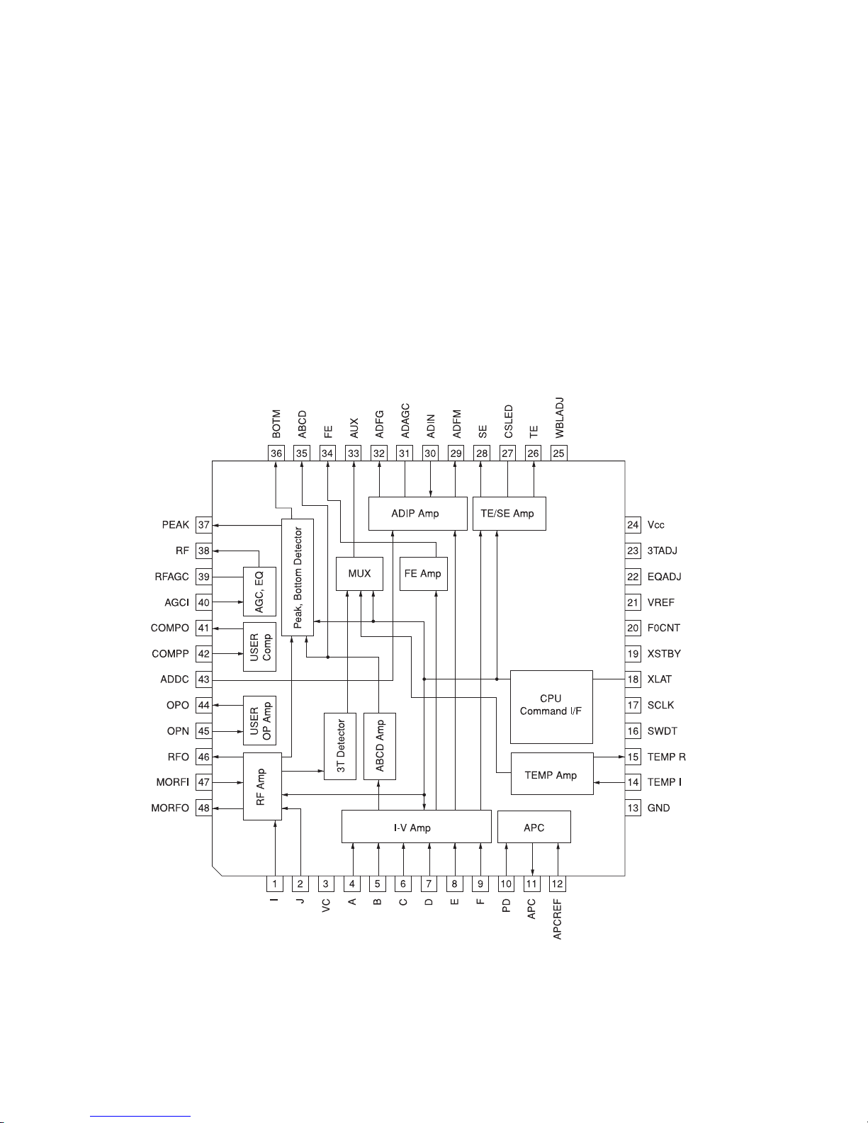
2) Automatic Adjustment Function
This mechanical module implements the following automatic adjustments using the RF amplifier, servo IC and
microcomputer. This function is intended at ensuring stable play by eliminating variations in sounds that can result
from conditions of given environment or discs as well as aged deterioration of the module.
Whenever a disc is inserted, this adjustment is carried out in the following sequence.
1) Offset adjustment
* Electric offset being output from the RF amplifier is adjusted to 0V seen from the reference voltage.
* This adjustment is automatically executed in the IC according to VC, FE and ABCD instructions from the microcomputer.
2) IV adjustment
* Gain of the RF amplifier’s current/voltage converter AD is adjusted to approximately 500 mV for pre_disc and
approximately 800 mV for rec_disc using the ABCD (full quantity of light) signal (64 pin) at LD_off as the reference.
* This adjustment is automatically carried out when the IC sends the command to the RF amplifier in response to the
instruction from the microcomputer.
3) Tracking balance (EF.B) adjustment
* In this adjustment, gain of E signal on the RF amplifier is varied so that TE signal may become evenly balanced
against VC (reference voltage, 67 pin) in terms of both plus and minus.
* This adjustment is automatically carried out when the IC sends the command to the RF amplifier in response to the
instruction from the microcomputer.
4) Focus AGC (F.AGC)
* This adjustment is done to maintain loop gain of the focus servo at a constant level so that stable focus servo
function may be ensured.
* Gain adjustment is done by injecting disturbance generated in the IC to the focus servo loop.
* This adjustment is automatically implemented by the IC according to the instruction from the microcomputer.
5) Focus bias adjustment (F.BIAS)
* This function is used for adjusting jitter of EFM signal to an optimum level by optimizing the focus point during play.
The microcomputer performs this adjustment by detecting phase and level of I3 signal from the RF amplifier and that
of FE signal.
6) Tracking AGC (T.AGC)
* This function maintains loop gain of the tracking servo at a constant level to ensure its stable function.
* Gain of the tracking servo is adjusted to a constant level by injecting disturbance generated in the IC to the tracking
servo loop.
* The IC automatically implements this adjustment according to the instruction from the microcomputer.
**** You can display and check results of the adjustment from the test mode (display in hexadecimal, 2’s complement)
"7F~0,FF~80" Conversion from hex to decimal
Hexadecimal ↓
"127~0,-1~-128" Decimal
1) OFST adjustment
Reference 00 (h)
Example 02 = VC ⇒2*13mV = +26mV
Result of the VC offset adjustment is +26mV, thus the circuit offset must be -26mV.
* Offset adjustment of FE and ABCD is implemented based on result of the adjustment done on the VC.
2) IV adjustment
Reference pre_disc: 16 (h) rec_disc: 08 (h)
Example 06 = 1V (with rec_disc) ⇒1 (dB)*(08 - 06) = +2dB
Gain is varied by +2dB against the reference value.
Gain is adjusted approximately by 1dB according to difference of steps from the reference. The smaller the value
represents higher gain.
3) EF.B adjustment
Reference 0F (h)
Variable gain volume can be computed based on difference from the reference.
Example 0A = EFB ⇒0.15 (dB) * (0A - 0F) = 0.75dB.
Gain of E signal is varied by -0.75dB against F signal.
(4) AGC adjustment
Reference 30(h)
Variable gain volume can be computed based on difference from the reference.
Example 27 = FACC ⇒20log (27 (h)/30 (h)) = -1.8dB.
Variable gain volume is -1.8dB. * The same applies to the tracking, too.
(5) Focus bias adjustment
Reference: 00(h)
Variable bias volume can be computed based on difference from the reference.
Example FA = BIAS ⇒FA(h) - 100(h) = -6.
Volume of bias applied = -6*13mV = -78mV.
1.2.2 Signal Processor Block
Data read from disc is conducted to RFIC, then entered to this IC as EFM signal.
The signal is subjected to EFM demodulation and ACIRC (error correction), then stored in DRAM once. As needed, the
signal is transferred from DRAM to this IC, and ATRAC expanded and then converted to audio data.
This data is output from the built-in DAC as analog audio data.
Incorporates a 20-bit DAC with an 8-times over-sampling filter and a secondary analog LPF (fc = 97 kHz).
9
CX-683
comp
RF
I
J
RF
amplifier
Pickup
amplifier
IC201
IC202
IC101
ATRAC DAC LPF
EFM
Demodulation ACIRC
Demodulation
DRAM
Memory
Demodulation
audio output
1.3 POWER SUPPLY AND DRIVER BLOCK (BA5985FM: IC401)
1) Power supply
Switched system power supplies MDVD and PVD (8.3V) from the mother board and backup system power supply VDD
(5V) are used for this system (see the power supply system diagram).
3.3V for driving MD/LSI system and LD is generated from MDVD. In order to drive large current, only PVD (3.3V) is
used as the driver power.
Pro-test is prepared to detect voltage error in MDVD.
As soon as overvoltage beyond 9.9V or undervoltage below 3.5V is detected, MD microcomputer turns off the start
control signal (VDON) from VD to stop supply of VD from the mother PCB.
In this case, ERR A0 indicating a power supply system error is displayed on the product.
2) Driver block
It is a linear driver used for driving 5 channels consisted of 1 channel on Load/EJ system and 4 channels on
actuator/SPDL/CRG system.
Forward/reverse drive (approximately 7.5V) of the Load/EJ system is implemented by the control signals (MLOAD AND
MEJCT) from the MD microcomputer.
4-channel system conducts binary PWM signal to the differential L.P.F, then supplies it driver.
You can monitor respective signals as analog signals (FIN, TIN, SIN and CIN).
10
CX-683
M
M
M
MEJCT
C+
C–
CIN
S+
S–
SIN
GND
LOP
LOM
SOM
SOP
COM
COP
MLOAD
T+
T–
TIN
F+
F–
FIN
GND
PVC
CONT
GND
FOM
FOP
TOM
TOP
CRG
SYSTEM
RC
LADDER
RC
LADDER
FOCUS
SYSTEM
RC
LADDER
SPDL
SYSTEM
RC
LADDER
PVD
LOAD/ET
Motor
SPDL
Motor
CRG
Motor
FOCUS
actuator
TRKG
actuator
CN401
LO+
LO–
SO+
SO–
CN101 F–
F+
T–
T+
SFDR
SRDR
SPRD
SPFD
< IC201 >
< IC201 >
< IC301 >
MD microcomputer
TRKG SYSTEM
TRDR
TFDR
< IC201 >
FFDR
FRDR
< IC201 >
11
CX-683
VD system
8.3V
ADD system
5V
3.3V
REG.
UPC2933T
BA5985FM
LD
RF·Amp
MD·DSP
PU/ACT
CRG/SPDL
MOT
MD micro-
computer
LogicBuffer
/mute
Load/EJ
MOT
* typ40mA
CXA2523AR
CXD2655BR
PD5541B
TC7WH125FU*2
SlaveP-Bus
DRAM
MSM51V4400DP-70TK
MDVD
system
PVD system DRIVER
8.3 ±0.5V VDsense
High : 9.9V
Low : 3.5V
Software protecting operation
* 5V drive during plays is also available
TEMP sense
+82 to 87°C
R314 : 10k 9.1k 8.66k
Thermistor 82°C85°C87°C
Output voltage 3.3 ±0.16V
1.3A with built-in excess
current protector
Software protecting operation
1.4 SCHEMATIC FLOW DIAGRAM FOR THE MODULE POWER
(TEMPERATURE DETECTION)
12
CX-683
2. MECHANISM DESCRIPTIONS
2.1 CARTRIDGE LOADING OPERATION
The load switch is provided in front of the cartridge transfer rubber roller.
The load switch is turned on after the cartridge is inserted. Turning this switch on will start rotation of the loading
motor-driven rubber roller and, as the result, transfer of the cartridge is initiated.
A view from the insertion port.
Load switch
(Normally off. It is turned on only when the
cartridge is inserted.).
A view from the insertion port
(when the cartridge is inserted).
Arm.=It starts rotating when the cartridge is
inserted.
An internal view of the machine. When the cartridge is inserted.
Loading motor Rubber roller
Eject switch (for positioning of the cartridge before ejection).
Cartridge insertion.
13
CX-683
2.2 CLAMPING OPERATION
The cartridge being transferred by the rubber roller pushes the resin lever shown in the figure. When pushed, the
spur gear on the resin lever (they are molded integral) is engaged with the rotating gear, thereby moving the
sheet metal lever fitted to the resin gear.
When the sheet metal lever is moved, the cartridge holder fitted to the groove on the sheet metal lever is driven
to the clamping position.
Cartridge being transferred.
Resin lever (being pushed by transferring force of the rubber roller).
Cartridge starts pushing the resin lever.
Sheet metal lever.
Resin lever (spur gear) after engagement.
Resin lever (spur gear) before engagement.
14
CX-683
Cartridge holder is driven to the clamping position by move of the sheet metal lever.
Left side fitting pin of the cartridge holder.
An internal view of the machine in the clamping operation.
2.3 EJECT OPERATION
The cartridge is ejected basically in the reverse order of loading.
Eject position is decided by the eject switch. As this switch is turned off, the loading motor is stopped and thus
the cartridge eject operation is completed.
Left side sheet metal lever.
Shutter is opened or closed by the shutter spring that is screw-fixed to the cartridge holder.
Right side sheet metal lever.
Arm for synchronizing the move of the left and right side sheet metal levers.
15
CX-683
3. DISASSEMBLY
-Removing the PU Unit
1. Provide short solder in section A, then remove the
connector.
2. Remove the two screws, then erect the board in the
direction indicated by the white arrow head.
3. Remove the two screws and two springs.
4. Drive out the PU Unit through the direction indicated
by the white arrow head.
-Carriage Motor and Spindle Motor
Removing the Loading Motor (1/2)
1. Provide short solder in section A, then remove the
connector.
2. Peel off solder in section B, then remove the lead
wire.
3. Remove the two screws, then dismount the MD Unit.
4. Remove the connector situated in section C.
Note: Before removing the Loading Motor, insert the
finished MD Unit, then clamp it.
CX-683
-Removing the Carriage Motor (2/2)
1. Remove the screw, then remove the Holder.
2. Remove the screw, remove the flat spring situated in
the position indicated by the black arrow head, then
drive out the Carriage Motor through the direction
indicated by the white arrow head.
-Removing the Spindle Motor (2/2)
1. Peel off solder provided in the circled position, then
remove the lead wire.
2. Remove the three screws, then drive out the Spindle
Motor through the direction indicated by the white
arrow head.
Note: When the PU Unit is installed, it must be
moved along the outer perimeter.
-Removing the Loading Motor (2/2)
1. Peel off solder in the circled position, then remove
the Flexible PCB.
2. Remove the four screws, then dismount
the Bracket.
3. Remove the two screws, then dismount
the Motor Bracket.
4. Remove the two screws, then dismount
the Loading Motor.
When replacement of the Loading Motor is
complete, apply 7V to the new Loading
Motor with the chassis being assembled
(without the MD Unit, though). Then, insert
the disk and clamp.
-Why clamping is required
It is difficult to dismount the Chassis Assy
from the Upper Case because its move can
be blocked by section A in the figure. As
long as the machine is in the clamp mode,
section A is pulled inside the chassis,
thereby allowing you to remove the chassis
easier.

Other Pioneer Speakers manuals

Pioneer XW-HT1 User manual

Pioneer

Pioneer XW-HT1 User manual

Pioneer S-IW40X User manual

Pioneer

Pioneer S-IW40X User manual

Pioneer XC-L11 User manual

Pioneer

Pioneer XC-L11 User manual

Pioneer Elite S-IW691L User manual

Pioneer

Pioneer Elite S-IW691L User manual

Pioneer CST S-IC651-LR User manual

Pioneer

Pioneer CST S-IC651-LR User manual

Pioneer Elite S-IW891 User manual

Pioneer

Pioneer Elite S-IW891 User manual

Pioneer ELITE VA-FW40 User manual

Pioneer

Pioneer ELITE VA-FW40 User manual

Pioneer XW-HTD640 User manual

Pioneer

Pioneer XW-HTD640 User manual

Pioneer TS-D690R User manual

Pioneer

Pioneer TS-D690R User manual

Pioneer S-HS01 User manual

Pioneer

Pioneer S-HS01 User manual

Pioneer HTV-SW2 KUCXC User manual

Pioneer

Pioneer HTV-SW2 KUCXC User manual

Pioneer S-DV77 User manual

Pioneer

Pioneer S-DV77 User manual

Pioneer S-DV390T User manual

Pioneer

Pioneer S-DV390T User manual

Pioneer PIONEER S-IC621D User manual

Pioneer

Pioneer PIONEER S-IC621D User manual

Pioneer XY-152-W User manual

Pioneer

Pioneer XY-152-W User manual

Pioneer MRX-5 Installation guide

Pioneer

Pioneer MRX-5 Installation guide

Pioneer SP-8603 User manual

Pioneer

Pioneer SP-8603 User manual

Pioneer SP-T22A-LR User manual

Pioneer

Pioneer SP-T22A-LR User manual

Pioneer XW-SX70 User manual

Pioneer

Pioneer XW-SX70 User manual

Pioneer S-DJ05 Assembly instructions

Pioneer

Pioneer S-DJ05 Assembly instructions

Pioneer XPRS10 User manual

Pioneer

Pioneer XPRS10 User manual

Pioneer TS-D1702R User manual

Pioneer

Pioneer TS-D1702R User manual

Pioneer XY Series User manual

Pioneer

Pioneer XY Series User manual

Pioneer Elite S-IC691A User manual

Pioneer

Pioneer Elite S-IC691A User manual

Popular Speakers manuals by other brands

Panacom SP-3481WMXL2 user manual

Panacom

Panacom SP-3481WMXL2 user manual

ITC T-200D owner's manual

ITC

ITC T-200D owner's manual

Konix ALL BLACKS HAKA ONE user manual

Konix

Konix ALL BLACKS HAKA ONE user manual

NHT OutdoorOne user guide

NHT

NHT OutdoorOne user guide

thomann the box speaker owner's manual

thomann

thomann the box speaker owner's manual

Konig CMP-SPSW150 manual

Konig

Konig CMP-SPSW150 manual

Audex SPB-2800 user guide

Audex

Audex SPB-2800 user guide

Centrios 4015115 user guide

Centrios

Centrios 4015115 user guide

JBL Harman Clip 2 quick start guide

JBL

JBL Harman Clip 2 quick start guide

EAW MQ1394e Specifications

EAW

EAW MQ1394e Specifications

Peaq PPA34BT-B user manual

Peaq

Peaq PPA34BT-B user manual

MartinLogan Center Channel speaker user manual

MartinLogan

MartinLogan Center Channel speaker user manual

Hitachi W50 owner's guide

Hitachi

Hitachi W50 owner's guide

OWI ST-73 Specifications

OWI

OWI ST-73 Specifications

TJ TS-G120 manual

TJ

TJ TS-G120 manual

Harman PRX908 quick start guide

Harman

Harman PRX908 quick start guide

Dynalink D 2038 operating instructions

Dynalink

Dynalink D 2038 operating instructions

MAGNEPLANAR MG1.6 instruction manual

MAGNEPLANAR

MAGNEPLANAR MG1.6 instruction manual

manuals.online logo
manuals.online logoBrands
  • About & Mission
  • Contact us
  • Privacy Policy
  • Terms and Conditions

Copyright 2025 Manuals.Online. All Rights Reserved.