Princeton 124A Service manual
,
.
"
Jan-29-02
ll:43A
MODEL
124A
LOCI<-IN AMPLIFIER
OPERATING
AND
SERVICE
MANUAL
-e-n~EGc.G
PRINCETON
APPLIED
RESEARCH
P.Ol
MDl12<11A.;
3/n·QQ
Copyrlc[email protected]&.QPRiNCETONAPPt..IlDRESEARCH Prtlt'lIJd In U.S.....

Jan-29-02
11'43A
P.02
SHOULD YOUR EQUIPMENT REQUIRE SERVICE
WARRANTY
A.
Contact
the
factory
(6091452·2111) or your
local
factory
-aprasantative
to
discuss
the
problem.
In
many
cases
It
will
be
possible
to
expedite
servicing
by
localizing
the
problem
to
a
particular
plug-in
circuit
board.
B. II it is
necessary
to
send
any
equipment
back
to
the
fac-
lory,
we
need
the
following
information.
(1)
Model
number
and
serial
number.
(2)
Your
name
(instrument
user).
(3)
Your
ecoress.
(4)
Address
to
which
instrument
should
be
returned.
(5)
Your
telephone
number
and
extension,
(6)
Symptoms
(in
detail,
including
control
settings).
(7)
""01,,11'
purchase
order
number
tor
repair
t.ha,rges
(does
not
apply
to
repairs
in
warranty).
EG&G
PRINCEtON
APPLIED
RESEARCH
warrants
each
tn-
strument
of
its
manufacture
to be
free
'rom
detect
s in
material
and
wcrkrnanshlp.
Obligations
under
this
Warranty
shall
be
limited
to
replacing,
repairing
or
giving
credit
for
the
purchase
prtce,
at
our
option,
of
any
instrument
returned.
freight
pr'£"paid,
to
our
factory
wtthtn
ONE
year
of
delivery
to
the
original
purchaser.
provided
prior
authorization
for
such
return
has
been
given
by
our
authorized
rapraaantauve.
This
Warranty
shall
not
apply
to
any
Instrument
which
Our
in-
spection
shall
disclose
10 Our saustecucn.
has
become
detec-
live
Or
unworkable
due
to
abuse,
mishandling,
misuse.
acct-
dent,
alteration.
f1egliger'ce,
improper
installation
or
other
causes.
beyond
Our
control.
Instruments
manufactured
by
cthera,
and
tnctuded
in or
supplied
with
OUf
equipment,
are
not
covered
by
this
Warranty
but
(:~HrY
tne
odginal
rnanu
tactur
era
warranty
which
is
extended
to
our
customers
and
may
be
more
restrictive,
Certain
subassemblies,
accessories
or Com-
ponents
may
bo
specifically
exctuded
from
tnts
Warranty,
ill
which
case
such
exclusions
are
listed
in
the
Inetructton
Manual
supplied
with
each
Instrument.
C, U,S,
CUSTOMERS-Ship
the
equipment
being
returned
to:
(8)
Shipping
instructions
(i1
you
wig
h 10
authorize
ship-
men.
by
any
method
other
than
normal
surtaca
transportation),
we
reserve
the
right
to
make
changes
in
design
at
any
nme
without
incurring
any
ohlig(:llion
10
install
same on
units
previously
purchased.
THERE
ARE
NO
WARRANTIES
WHICH
EXTEND
BEYOND
THE
DeSCRIPTION
HEREIN.
THIS
WARRANTY
IS IN
LIEU
OF.
AND
eXCLUDES
ANY
AND
ALL
OTHER
WARRANTIES
OR
RePRE-
SeNTATIONS,
EXPReSSED,
IMPLIeD
OR
STATUTORY.
IN·
CLUDtNG
MERCHANTABILITY
AND
FITNESS,
AS
WELL
AS
ANY
AND
ALL
OTHER
OBLIGATIONS
OR
LIABILITIES
OF
EG&G
PRINCETON
APPLIED
RESEARCH.
INCLUOING.
BUT
NOT
LIMITED
TO.
SPECIAL
OR
CONSEQUENTIAL
DAMAGES.
NO
PERSON.
FIRM
OR
CORPORATION
IS
AUfHORllED
TO
ASSUME
FOR
EG&G
PRINCETON
APPLIED
RESEARCH
ANY
ADDITIONAL
OBLIGATION
OR L1ABII,.ITY
NOT
EXPRESSLY
PROVIDED
FOR
HEREIN
EXCEPT IN
WRITING
DULY
EXE·
CUTED
BY AN
OFFICER
OF EG&G
PRINCETON
APPLIED
RESEARCH.
FG&G
PRINCETON
APPLIED
nESEARCH
P0
Bo'
2565
Princeton,
NJ
085~.J
phone:
609/452-2111
TELEX:
84
3409
Address
corr
e
spondence
10:
EG&G
PRINCETON
APPLIED
RESEARCH
7R(lSzel
Road
(Off
Alexander
ROCld,
East
of
Route
1)
Princeton,
New
Jersey
D.
CUSTOMERS
OUTSIDE
OF
U.S.A.-·To
avoid
delay
in
customs
clearance
of
equipment
being
returned,
please
contact
tile
rectory
or
the
nearest
factorv
dtstnbutor
for
complete
shipping
information,
E.

Jan-Z9-0Z
11:44A
TABLE
OF CONTENTS
•oection Page
CHARACTERISTICS
1·1
'_1
Introduction
1-
1
1.2 Specifications:
1-3
1.2A Signal
Channel
Specifications.
1-3
1.2B Reference
Channel
Specifications
1-3
1.2C
Dumodul
ator
Characteristics
1·3
1.20
Outputs
1·4
1.2E Dvnernic
Rcmge
Specifications
1-5
1.2F Other Characteristics
1-5
II
INITIAL
CHECKS
11·1
2.1
Introduction
11-1
2.2 Equipment Needed
11-1
2.3 Procedure
11-1
III OPERATING INSTRUCTIONS
111-1
3,1 Block
Diagram
Discussion
111-1
3.1A Introduction
111-1
3_1B
Signal
CharH"H:~1
111-1
3_'C
Reference
Channel
111-1
3_10 Synchronous
Detector
111-1
3.2 Signal Channel
Operation
111-3
3_2A Introduction
...
111-3
3.2B Preamplifier Choice
111-3
3.2C
Grounding
111·3
»
3.20
Remote
Preamplifier
Adapter
111-4
,,'3_2E Sinqle-Endsd, Differential. and Transformer Inputs
111-4
:l2F
Common-Mode
Rejection
111-5
3_2G
Noise
and
Source
Resistance
111-5
3.2H Selectiv@
Amplifier
111-6
3_21
Dvnarnic Range
111-13
3_2J
Dvnamic:
Over-ride
111·15
3_2K Overload
111,15
3_2L Offset Due to Noise
111-17
3.2M Overload Racnverv
111-17
3.2N
Signal
Monitor
111-18
3.3
Reference
Channel Operation
111-18
3,3A
Sync
Input/Output
111-'8
'.3.3B
Phase
Control'
111-19
3A
Outpu
t Channel OPeration
111-21
4AA
Filter Time
Constant
111-21
3AB
Offset Controls
111·21
3_5
Harmonic
Response
111-21
3_6 Sensitivity and Notch Calibration
111-22
3_7
AC Voltmeter Operation
111-23
3_8
Digit(ll Panel Meter
Modification
111-24
3_9 "./
Phase
Me
aauremerrts
111-27
3_10 Rear Panel Connectors
111-28
3,lOA
Interlace Connector (J9)
III-n
3,1011
Ext. Time Constant
111-29
3,11 Flattery Operation
111-29
3.12
Phase
Modification
111-29
)
P.03

Jan-29-02
11,44A
P.04
3.13 Mixer Monitor Mo<lifiCiil(ion
111-29
3.14 Remote Programming Option Modification
111-30
3.15
Selective
External
Reference
Modification
11I·31
(
IV
ALIGNMENT
PROCEDURE
IV-'
4.'
Introduction
IV-'
4_2
Equipment
Needed
IV-'
4.3 Procedure
IV-'
4.3A
Preliminary
Steps
IV-'
4.3B ±24 V Adjustments IR6028 and R60101- Power Supply Board
IV-'
4.3C
Initial
Reference
O~cillator
Board Adiusrmanrs IV·3
4.3D Auxiliary
Reference
Board
Adjustments
IV-3
4.5E Mixer Board
Adjus
tmenrs
IV-4
4.5F
lntermediate
Amplifier Board Adjustments IV-5
4.5G Final Reference Oscillator Board
Adjustments
IV-5
4.5H Signal Board Adjustm@llts IV-5
4.31 Final
Adjustments
IV-6
4.3J Phase
Meter
Option
Alignment
IV-6
4.4 Model 116,
"7,
or 119 Preamplifier Alignment IV-7
4.4A
Preliminary Steps IV-7
4.4B Procedure IV·7
4.5
Model
118
Preamplifier
Alignment
IV-8
4.5A
Preliminary
Steps IV-B
4_5B
Procedure IV-8
V
TROuBLESHOOTING
_v.t
5_1
I
ntrod
ucnon
_
V·l
5.2
Equipment
Required .
V-'
5.3 Initial
Steps
V-'
5,4
Power
Supply
_
V·l
5.5 Reference Checks v-t (
5_6
Signal Channel V·3
5.6A
Preamplifier
V-3
5.66 Signal
Arnplifier
V-3
5.6C
Intermediate
Amplifier
V·S
5.6D Mixer Board AC Gain V·S
5.6E
Mixer
Schmitt
Triggers V·5
5.6F
Mixer
Circuit
V-S
5.6G DC Ampltflers V·6
5.7 Noise Checks V·6
VI SCHEMATICS, TABLE OF
VI-l
c

»
Jan-Z9-DZ
11:44A
FIGURES
'.Imber
1-1
Model 124A Lack-In Amplifier
1·2 SYnc. Signal Slewing Rate
1·3 Typical Calibrator
Accuracy
111-1
Functional
Block Di.gram, Model 124A
111-2
Optimum Performance Regions
of
the Prearnpfifiers
111·3
Distortion
v,
Frequency,
Model
118
.
lirA
Ground-Loop
Voltage
Heiection
Using Di
tferenttal
Inputs
111-5
Model 183 Remote Preamplifier
Adaoter
111·6
Typical
Common-Mode
Rejection
....
__
....
III· 7
Tvolca!
Noise Figure Contours for Model t17, Model 116 (Direct! and Model 119 (Direct)
11I·8A
Typical Noise Figure
Contours
for
MOdel
116
Operatinq
in the Transformer Mode . .
111·86
Typical Amplitude Transfer Curve, for Model 116 Operating in the Transformer Mode
III-SA
Tvpicat
Noisl! Figure Contours for Model 119 Operating in the Transtorrner Mode , .
111-98
Typical
Amplitude
Transfer
Curves for Model
119
Operating in the
Transformer
Mode
111·10
Typical
Norse Figure Contour's for
Model
118
, ,
__
,
..
111·11
ATvpical
NoiSe
Figure Contours for Model 190 Transforrner-Plus-Preamptitier
111-118
Model 190Wiring Diaqrarn
If
l-t
l C
Tvpical
Amptirude
Transfer Curves for
Model
190
111-11
D
Photo
of
Model
190
Transformer
111-12
S-H
Curves and Waveforms
111-13 Degaussing
Wetveforr'J)s
111·14
Model
124A
BandpassCharactaristics
111-15
Model 124A Notch Characteristic'
111-16
Model
124A
Low
Pass
Characteristics
111-17
Model 124A High Pass Characteristics
111·18
Dynamic Range Cnaracteristics of the Model 124A
1-19 Typical
Output
Offset as a Function of Input Noi,e
111-20
Typical
Reference Oscillator Slewinq Rate
111-21
Net
Phase
Difference
Between Signal and Reference Channels as a
Function
of Frequeucv
111-22
Output
Filter Transfer
Function,
_ .
111-23
Tvpical
Calibraticn
Accuracy _ _
111·24
Mixer
Output
for In-Phase and
Quadrature
Signals
IV·l
Model
124A
Adjustments. ijlnrj Testpoinrs
TABLES
Number
P.DS
Page
1·2
1-4
1-5
111-2
111-3
111-3
111-4
111-4
111-5
111-7
111-8
111-8
111·9
111-9
111-10
111·11
111-11
111-11
111-11
111-11
111-11
111-12
111·12
111·12
111·12
111-
14
111-17
111-18
II1·19
111-20
111·24
111-29
IV-2
Page
,
1-1
1·2
I"
-1
111·2
111-3
111-4
111-5
11I6A
111·68
111-7
II1·8
111·9
V-I
Praarnpfifiar Specifications
.,
,
...
__
, .
Model
124A
Dynamic: Range Specifications
Stability and
Output
Noise as a Function
of
Operating
Dynamic
Tradeoff
Maximum RMS
Input
Levels for
Mixer
and
Tuned
Amplifier
Overload as a
Function
of
Sensitivity and Operating Dynamic Range _
Maximum
Frequency
Acquisition
iime$
of
Oscufator
.
Typical Harmonic
Response
Operating in the
Flat
M<'H.:I~
Typical
Harmonic
Res~onse
Oper
atinq in Bandpass
Mode
with
0-10
Digital
Output
Pin Assignments
Digital
Output
Truth Tables _ .
Interface
Connector
Signals and Pins .
External
Time
Constent
Connector
Signals and Pins
Remote
Programming
Connector
Pin Assignments
Gain and Relay Switching for tho Model 124A
.
1-1
_ 1-5
111-
15
111-16
111-19
111-22
111-22
111-25
111-26
111·28
II 1·29
111-30
. V·4
Jan-Z9-0Z
11:45A
SECTION I
CHARACTERISTICS
P.06
1.1 INTRODUCTION
The
Model
124A
Lock-In
Amplifier
accurately
me asures
the
rms
amplitude
and
phase
of
weak
signal~
huried
in
noise.
Signals
in
the
range
of
picovol
ts
up
to
500
millivolts
at
freouencies
from
0.2 Hz to
210
kHz Can be
measured
quickly
and
precisely.
Meter
and
voltagp.
outputs
are
provided
for
the
amplitude,
arid
t1H~'
phase
of
the signal
m<1Y
be
read
from
a
dial.
These
measurements
are
with
reference
to
~
wnchronjzjqg
signal
supplied
to.
or
supplied
by,
the
Model
124A.
In
either
the
External
or
External
f/2
mode
of
op~ratiorl,
the
instrument
will
accept
any
rl?ferel~~
wave-
form
that
crosses its.
mean
twice
each
cycle,
and will lock
to
and
track
that
signal
OVC(
a
100:
1
frequency
range.
In
the
Internal
mode,
the
frequency
is
determined
by
front-panel
dials
or
by
an
externallv
derived
voltage,
A
selection
of
ptuq.in
preamplifiers
is available
for
pro-
vidinq
optimum
low-noise
performance
Over a
wide
range
of
input
frequencies
and
source
resistances:,
After
preampll·
ficatton.
noise
and
harmonics
acccmpenvinq
the
signal are
attenuated
in
the
Signal
Channel
by
filtering
out
all
frequencies
except
the
band
in
which
the
signal lies.
Flat,
band
Pass.
band
reject,
high
pass,
and
low
PHSS
filtering
modes
may
be
selected.
The
remaining
band
of
frequencies
is
converted
to
an
equivalent
bandwidth
about
de
by a
-vncbrrinous
detector.
which
is
locked
to
the
svnchronlztnq
qnat.
A
low-pass
filter
elirnirlatEi!s
frequency
components
above de,
,0
that
the
detector
output
is a de voltage
propor'tional
to
th~
in-phase
component
of
the
fundamental
signal. Propi:!r
selection
of
signal
channel
and
output
channel
filtering
parameters
can
render
the
final
noise
bandwidth
extremely
narrow
_
The
rrns
value
of
the
[unda-
mQrHal signal is
indicated
on
the
pal'l~1
mater
when
the
synchronous
detection
phase
is
adjusted
for
maximum
detector
output.
ASWitch is
provided
that
allows
drift
to
be
traded
tor
dynamic
reserve. In
addition.
an
output
de
offset
ff;!atul"I~;
is
provided
to
allow
higher
sensitivity
settir1gS for
relatively
steady
signals, These
fe<1ture~
permit
selection
of
the
optimum
opcr
atinq
mode
for
each
experimental
situation.
Other
de:;igr"l
fcaturas
include
selection
of
output
filter
lime
constants.
to
300
seconds,
optional
digital
panel
meter
with
BCD
output,
ij
built-jrl
calibrator.
and
independent
use
of
the
phase-lockable
oscillator
and
tuned
amplifier
for
general-purpose
laboratory
work,
The
Model
124A
","y
also
be
used
as a
conventional
wideband
laboratory
voltmeter.
Accessories
include
an ac
zero
offset,
several
light
choppers.
a
computer
interface
system.
and a
wide
assortment
Of
low-noise
preamplifiers.
Specification
Model
116
Model
117
Model 118 Model
119
Input
Z
Selected
by
front
panel
switch:
100
meqohrns
SEIDE
Direct;
100
rneq,
SEIDE
Transforrnere:
Low
Z
SEIDE
10 kilohm'S
SEIDE
Selected
by
front
panel
switch:
Direct;
100
rneq,
SEIDE
Transformer:
Low Z
SEIDE
Bandwidth
Direct; 0_2 Hz -
210kHz
0.2
Hz ..-
210
kHz
0.2
Hz -
210
kHz Direct;
0.2
Hz -
210
kl-lz
Transfcrmerb: 1.5 H.z:-l0 kHz
Transtormerv.
1
kHl-210
kHz
Common
Mode
Direct:
120
dB
at
60
Hz
120
dB at
60
Hz 110 dB at 60
H,
Direct;
120
dB at
60
Hz
Rejection
Ratio
Transformar:
140
dB at
60
Hz
Transformer:
120
dB at 60 Hz
Full
Scale
Direct:
100
nV
100
nV 10 nV Direct;
100
nV
Sensi tivi tv Tr anstor
mer:
1
nV
aTr ansforrner: 1
riV
MaximLlm
Input
Direct:
i200
V de
±200
V de ±5 V Direct:
±200
V de
Voltage
Transformer:
tn
mv
rrns
Transformer;
10
mV
rrns
sine wave
sine
wave
ay
b.
wired for
1:50
to
1:350
turn,
ratio.
Stand,,,d
is
1:100.
"varies
with
source
Impedance.
NOTE:
A cur
ten
t-sensi
tive
preamplifier,
Medel
184,
is also
available.
See
ACCESSOR
IES list
at
end
of
specs,
."
Table
I.'.
PREAMPLIfIER
SPECIFICATIONS
1-1
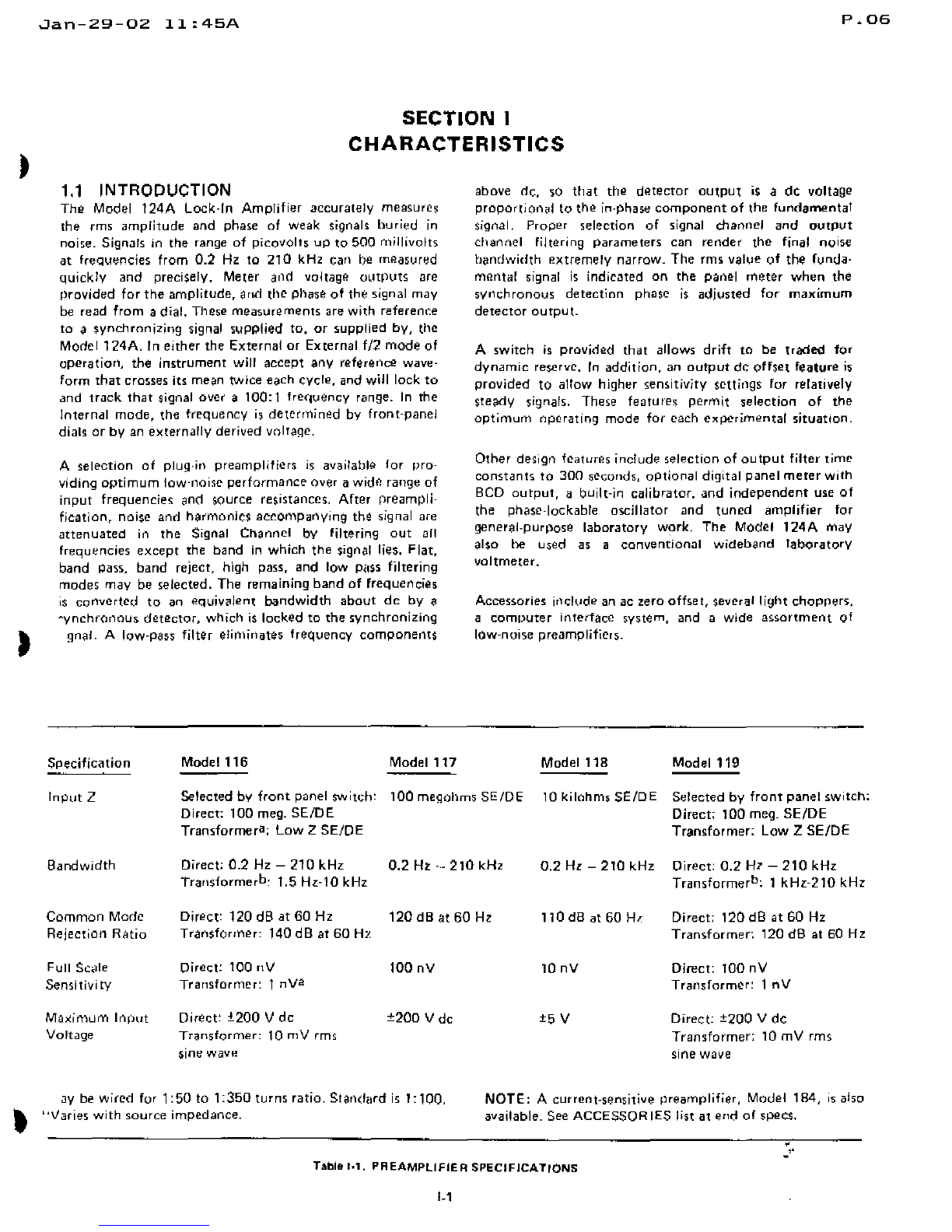
FREQUENCY RANGE
fig.,"
1-1.
MODEL
124.0,
LOCK·IN
AMPUflER
il
>
o
'-J
-1>
U1
:t>
'"
'"
t,
III
:lI
N
Ul
I
o
N
SELECTS
INSTRUMENT
FUNCTION. IN AC
FOSlnON~
..
CTS
"5
W'QEB"NO R
MS
VOLTIWETER. IN PSO
POSITIONS,
ACTS AS
l..OCI<·lN
A~PlIFIER
-
LECTS CA.L.
VOLTA.GE CAL.
IN BAN0 PASS
SWIT... HIGH
(l
AVE~
AGE
-
AEADJ
NG
METER
CA.L.lB;ftATEO
~N
RMS
FOR
SlNE-
WAVE.
If!lPUT
LI GHTS IF REf. OSC.'S NOT
FREQ.
LOC~ED
TO REf. 'NPUT.
OQES
NOT
mo
ICATE PH
A.SE
UNl.OCK
/OVERLOAO
INDICA.TOR
"'
...
_-~
/----
-.-
CRANII(S IN de OFFSET IN
f'RONi
OF
O'JTPLT AMPLIFIER. I
TURN'
IFULL SCA.LE,
FOR A
Tcrr"L
OF
'0
FULL SCALES.
TOGGLE SELECT POL..RI
TY.
SELECTS TIME
CONSTANT
OF OUTPUT
LP FILTER. S OR
II
dB/ OCT"VE
ROUOFF
SELECT PHASE OF SYNa-lRONOUS
DETECTlON
wml
RESPECT TO REI'
,,-
SELECT
E~"CT
FREe<UENCY
OF
esc:
LLA
TOR IF OPERAnNG IN
INTERNAL
MOOE.
NOT FUNCll ONAL
WHoN OPERATI
~G
IN
o~1lERN"L
o.IOOE
AOJUST FOR ZERO
TR"NSFER or CENTER
FREQUENCY
IN NOTCH
MOOE
SELECTS
sH
A.RPN
ESS OF
SELECTIVE
A.M
PLIFIER
e<'
lIto
13dB
OSC.
RANGE.
OECIMA.L
IN Ex:TERNAl POINT
MaOE SET TO
EXPEhEO
RANG.~i
OS(;.
PHA.SE
-LOCI<>
AU
TOMA
TIC
ALLY,
NULTI PLIEiR IN tNT.
SELECT EXACT CENTER
FREQUENCY
OF SELECTIVE
..MPLIFIER
..t.
REFERENCE
INPUT
TO
WHICH OSCILLATOR
LOCKS.
osc.
LOC
KS TO
POSITIVo-GOIPlG ZERO
CROSSING
e
SELECTS 'OPERATI"G
MO
OE
OF OSCILLATOR.
IN
"Z
PQSITIO!',
osci
LLATQFl'
LUt,;:KS
TO
SECOND
IIAR"'ONJC
.1',)\,
'W._.~
.
@-
'"
~
•
USEO 'WHEN
CALIBRATING
SiENSITlVITV
SELECTS
OPERATING
MOOE
OF SIGI>IAL
CHANNEL
~
~
\
'=:-"
I'Q'r
"-
"
O
"'
_
oUOO'
PLUG-liN
PRt:AMP'.
-..,
..
MODEL 116,I
~
7,
lie
.-,
__
-...-.
OR
119.
SELECT
ACCORDING
TO
FREe<.
RANGE
ANO
SOU~CE
'''PEOANCE. SEE
SPECS.
MOOEL II S
INCREA5ES
OVERA.LL
5ENS. BY
l(
10.
N

Jan-29-02
11'45A
1.2
SPECIFICATIONS
1.2A
SIGNAL
CHANNEL
SPECIFICATIONS
-"
Frequency
Aange
Model 124A; 2 Hz -
210
kHz
Model
124AL:
0.2
Hz -
210
kHz"
Sensitivity:
21 full-scale
ranges
in 1-2-5
sequence.
Full-scale
vol taqcs
are
determined
by
the
choice
of
pre
amplifier
,
Ser~$it.ivity
and all
other
preamplifier-determined
specifi-
cations are given in
Table
1.1.u
Sign,,1
Channel
Modes
of
Operation
(1)
FLAT:
Flat
response
within
±1%
from
10 Hz
to
110
kHz. ±2% from
110
kHz
to
210
kHz. and ±10% below
10 Hz.
P.OB
0.01%.
The
frequency
stability
is
typically
0.05%
of
the
set
freq\Jency.
121
EXTE
RNAL'
The
internal reference oscillator will
lock in
both
trequencv
end phase
to
virtually any
extemaltv generated signal crossinq its mean onlv
twice
each
cycle.
Maximum
input
voltage
is
±20
V
de.
Minimum
time
required
on
either
side
of
the
mean
is
100
ns.
Amplitude
excursion must be
at
lean 50 mV
abovo and
below
the me
en.
rnou tirnpedanee is 1
r'r'n~
go hrn.
When
locked
on,
the
raferunce
oscillator
will
track
the
external
signal
over
a
frequency
range
of
l00~
1
within
the range of
the
set band of
frequeneie~.
Ma.imum
frequency
acquisition
(lock-on)
times
for
each
fre-
quency
band
are
given
in
the
following
table.
FREQUENCY
RANGE MAXIMUM
TIME'
•
121
BANDPASS;
Provide'
a
tunable
bandpass response
with
the
center
frequency
set by
front-panel
digital
dials
o,v"
aranqe
of
2 Hz to
110
kHz. Setting
accuracy
-is
within
12%
Or
0.05
Hz,
whichever
IS
greater.
Bandwidth
is adiustable over a
rang~
of 1% to
100% (at 3dB
points).
corresponding
to
a range of Q
between
100
and 1. by means of
the
front-panel
Q
control.
(31
NOTCH, Essentially
the
same as
the
Flat
mode,
but
with
the
addition
of a
tunable
notch
that
provide,
up
to
80 dB
of
attenuation
at
any
specific
frequency.
The
notch
is
tuned
with
the
same
controls
as
set
the
bandpass frequency.
BAND
Xl .
Xl0
.
Xl00
.
Xl K .
XlO
K .
0.2
Hz
to
21 Hz .
2 Hz
to
210
Hz .
20Hzto2.1
kHz
..
200
Hz
to
21
kHl
.
2.1 kHz to
210
kHz .
15
minute,
2
minutes
10 seconds
2seconds
2
seconds
(4) LOW PASS, Essentiellv
the
same as
the
Flat
mode,
but
with
the
addition
of
alow pass. filter
that
provides
a 12 dB
per
octave
rctlott
a~)ove
the
set freqv(!'lCY.
(51 HIGH PASS, Essentiallv the same
a'
the
Low Pass
mode,
but
with
the
substitution
of
a
high
pass filter in
place
of
the
low
pass filter.
1.2B
REFERENCE
CHANNEL
SPECIFICATIONS
Modes
(1)
INTERNAL:
Frequency
of
the
internal reference
oscillator
is
set
by
means
of
fr
ont-panat
digital
dials
and/or
rsar- panel VCO
control
voltage,
Setting
accu-
racv is
within
±2% Or
0.05
Hz,
whichever
IS
greater.
veo
control
vcttege
of 0
to
±10 V
corresponds
to
the
full
frequency
range
on
all bands. VCO
input
irnped-
ance is 10 kilohrns.
The
amplitude
stability
is typically
°
Modtill
124AL
h;]5
5igrlifi!:::;!IlltIV
lunasl'
severe-over
toad
reCO\lllrv
nme
(80
s n
30
5
with
~OOO
limes
1ull
$clIle
OV8,IoOid
for
onljl
""'11'l1J~el
.
••
Two
additionOiI
prel
...
rnplifier5.
th e
Modal
lB4
;lind
thll
Modilll
186,
£Ira
evauetne.
r-or
informatIon,
c
oo
tac
r (118
hlctOrV
or
the
eecro-v
re~r65ti1rHlItivl!!r
in
vo
ur
IIrl!rll.
1·3
Once
the
frequency
hJS
locked,
the
phase
will
track
at
the
rate
shown
in
the
diagram
on
the
following
page.
Phase
Adjustment:
Calibrated
10
turn
potentiometer
pro-
vides 0·100<)
phase
shift.
Linearity of phase
setting
is
within
±2Q
from
2 Hz
to
21
kHz,
and
within
±5°
from
21
kHz
to
210
kl-lz.
Resolution
is D.1Q•A
four-position
quadrant
switch
provides
901'
phase
shift
increments.
1.2C
DEMODULATOR
CHARACTERISTICS
ACVM;
An
ACVM
position
on
the
function
switch
permits
the
Model
124A
to
be used as a convenrional or
Irsquencv-
selective ac
voltmeter.
Accuracy
is
within
±1%
from
2.
H2
to
20 kHz, increasing
to
±10% at
210
kHz.
Dc
Output
Stability
and
Noise'
Dependent
on
the
oper.ting
mode
selected
by
the
front-panel
Function
switch,
as
shown in
the
Stability
&Noise Tobie
(next
pagel.
"Timl!l
cOIn
bll
$hQrtanl;td
.!I~p(ecillbIV
by
r~lUmelHlIl'ily
switehino
(0
lntl!lrnollli
Modll
IjInd
rnal'llJll!llIy
1-ettir"lQ thE!
csc
Hta
ror
to
ene
pr
eper
're~uencY.

Jan-29-02
11'46A
P.09
(
"o~
o
"
,.
00'
l'.5
~
o·
..
-,
!il
..
"'
w
-O<f.
..
..
~
..
•
"
-180
XI
-0,004
-0,003
-O·QO~
~O.OOI
0
0.001
0.002
0.003
0.00"
..
"'0
-0.'
-0,3
-O·~
- 0.1 0 0,1
O.~
0.3
0.'
..
~
..
z
..
.". XIOO
-.0
-30
-'0 -'0
0
'0
~o
z'"'
30
'0
"II:
""
""
X"
-
..
-30
-h
-" 0
,.
~.
..
••
.".
....
""
....
XIOII ..
11S'
""32.
"IU
-44t
~
..
0
•••
."
l!Jh
1711!i1l:
..
"
,,~
SY~c.
$IGiU.L
SLEWINt:i
,u.Tf:
IHi:ISE;CO-'O
Figurl!ll-2.
SYNC,
SIGNAL
SLEWING
RATE
Function
LOW
DRIFT
NO~MAL
HIGH DYN
RANGE
Output
Stability
<150
IN
I"c
<1
rnV/"C
<10
mv / "c
<100J.lV
rms
<1
mV rms
<10
mV rrns
Equtvute
nt
Noise
Bandwidth:
416
,u:Hz
minimum
(300
s
time
constant
with
12
dB/octave
rolloff).
Zero
Suppress:
Calibrated
control
permits
off-setting
zero
by ".1000% 01 lull scale on
Normal
and High
Dynamic
Rang.
only.
•
Demodulator
Overload
Limits:
Dependent
on
Function
switch
setting
as
follows
(see
Subsection
3.21
for
over-ride
conaider
at
ions).
LOW
DRIFT
,
..
, . . 10 xlull
,cal.
NORMAL
,.
.100 xlull scale
HIGH DYN
RANGE
,1000 xlull scale
System Gain
Stability;
100
ppm/
aC; 100
ppm/24
Hr in the
Flat
mode
and
with
Function
switch
set
to
NORMAL.
1-20
OUTPUTS
ME!ter Redding: Choice
of
either
center-zero or
lcf
thand-
JP.ro
panel
meter
of
taut-band
construction.
providing
0.5%
linearity.
This
limit
is
defined
CIS
the
ratio,
at
1I~(!
input.
of the
maximum
pkpk
voltage
of a
non-coherent
signal,
before
overload,
to
the
pk-pk
voltage
of a full-scale
coherent
slnewave.
Note
that,
in
terms
of
pk-pk
noise
to
rms Signal.
the
instrument
will
accept.
without
overload,
interfering
Signals
having
E1n
amplitude
up
to
3000
times
the
sensitivity
sc
ttinq,
(See
discussion
in
Subsection
3,21.)
OPtional
Digital
Readout:
file
Mo,I.1
124/\
may
b.
ordered
with
an
optiunal
diqit
al
readout
in
place
of
the
standard
panel
meter.
TIle
readout
is a 3% digit
display
with
a
linearity
of
0.05%
of
the
reading,
±1
count.
In
addition,
a
BCD
output
is
provided
at
the
rear
panel.
The
output
levels
are
DTLlTTL
compatible:
Logic 0=+0.2 V±0.2 V, 5mA
maximum
sinking
current;
Logic 1=
4-3.5
V
±l.O
V, 100
flA
maximum
sour
cinq
current.
Filter
Time
Comt;jlnb:
1ms
to
300
sin
1-3-10
sequence.
and
a mi
nlmum
time
constant
posltlon
having
a
time
constant
of
less
than
1rns
[daterrruned
by
internal
stray
capacitnnce}.
n1E~
External
position
allows
capacitance
to
be
added
via a
rear-panel
connector"
to
obtain
special values
of
time
constant.
Either
6
or
12
dB/octave
r
ollotf
as
selected
by
means
of
front-panel
switch
is pr
ovtded.
-
MI!.".uured
with
li''''''1iiI
(,QI"Ist.mt
of
1 S
Itnd
12
dl3!OCTilv\llulloff,
Function
Out;
Ade signal corresponding to
the
panel-meter
rcadinq,
An
output
of 10 V
corresponds
to full-scale
deflection.
'The
output
impedance
is 1
1<>11.
Signal
Monitor:
Enables
continuous
monitoring
of
the
signal
channel
output
ahead
of
the
demodulator.
In LO
DRIFT
operation,
a full scale rrns
input
sf
newave
gives a
100
mV
rrns
sinewave
at
the
Signal
Monitor
jack.
In
NORMAL
operation,
the
signal
monitor
output
with
a
full-scale
input
is 10
mV.
and
in HI, it is 1
mv.
Dvnernic
(
1-4

Jan-29-02
11:46A
Operating
Dynamic
Range
Tradeoff
LO
DRIFT
NORMAL
HI DYN RNG
[Reserve]
Output
DYna(r'li~
Range
6_6 X10"
10'
10
3
PSD
Dynamic
Reserv'!!
10
10'
10'
PSD
Dynamic Range
6_6
x
10'
10'
10'
Total
Dynamic
R.iUig~
6_6 x
10'
10'
10'
P.I0
Table
1-2.
MODEL
12.11A
OYNAMIC
RANGE
SPECIFICATIONS
Over-ride considerations
apply
as
explained
in
Subsection
3.21.
Output
impedance
is 600 n.
Internal line
frequency
pickup
is less
than
20 nV rrns
(referred
to
the
Direct
inputs
of a
Type
116
Preamplifier)
in
any
Signal Channel
mode
except
Bandpass
and
Notch,
where
the
level
may
rise to
500
nV at
highest
0
settings.
Hefarance
Channel: Asinewave
output
at the
reference
oscillator
frequerlC.~V.
Amplitude
is.
contmuouslv
adjustable
by
means
of
the
front-panel
Level
com-o!
over arange of
oV
to
10 V
rms
with less
than
2%
distortion.
Output
impedance
is 600 ohms.
.'"
;!
e10
·
C
·
1.01
'±10
•
?
~
i
!O,l
0'
.'
,,'
~.
)
1.2E
DYNAMIC
RANGE SPECIFICATIONS
Vary
as a
function
of
the
operating
Dynamic
Range
Tr
edeoff
as
indicated
in the
table
above.
..LF OTHER CHARACTERISTICS
Overload:
Front-panel
light
indicates
overload
at
critical
circuits.
Reference
Unlock;
Front-panel
light
indicates
that
the
reference
oscillator
has
not
completed
Irequeucv
lock.
Internal Calibr.ator: Square-wave calibrator signal supplied.
Rm5
amplitude
of
fundamental
frequency
component
sdjust
atuc
from
20 nV to
100
mV in 1-2-5
sequence.
Tvpical
accuracy
indicated
in
Figl.Jr~
1-3.
Ambient
Temperature
Range:
Unit
can
be
operated
at
ambient
temperatures
ranging
from
15°C
to
45°C.
Auxiliary
Power
Output:
Regulated
t24
Vat
uo
to
100
mA
is available at rear-panel
connector,
Power
Requirements:
105-215 or
210-250
V; 50-60
HI;
unit can also be powered from batteries. by supplvinq
t31
V
to rear pdnel
connector.
Bi:ltterie~
must
be able to
supplv
at
least
400
mA at +31 V and
360
,~A
at
-31
V.
"NOT!::::
ThA'l;II ./:If'1
maxrrnu
m
values
anu
do
nut
eootv
ro
r
~II
POSI~Il)nfj.
01
the
SenSITivity
swttcn.
for
8
g",n",ral
(hii(:~Jjj.~lon
of
yhll
rTHHllning
at
these
ter
ms
IlI"IIJ
Hllllllr
Ilgnifil:;<lnce,
~ee
Appendix
A
A1t
thl!
,IISf
Of
thl~
manual,
,A I
so.
Gee
Subsllllcticrl
3.21.
1-5
fi9ur'J 1-3.
TYPICAL
CALIBRATOR
ACCURACy
Size: 17-1/8"
W,
7"
Hx18-114" 0
(43.6em
W,
17.8 cm
Hx46,5 em DI.
Weight: 34 lbs 115.5 kg!.
Accessories: Model
173
AC
Zero
Offset
provides
square
wave at
the
reference
frequency
which
can
be
used
to
suppress siqnals at the
input
of
the
Model 124A_
Other
accassoriss include a
computer
interface
system,
fixed
and
variable:
speed
I
ight
choppers,
and
abroad
selection
of
special purpose pre
ampfttlers.
The
AM-1.
AM-2.
and
190
input
transformers
allow
better
noise
performance
to
be
achieved
when
~Jsing
a
hiqh-input
impedance
preamplifier
to
process a signal arising in a low
source
impedance.
The
Model
184
Current-Sensitfve
Preamplifier
is also
available. This
prear'r1~)lifier.
which
plugs
i"
like
the
Models
116. 117.
118.
and
119
Preamplifiers.
provides 1 V
out
for
input
currants
ranging
from
1 nA
to
10
J.1A
<IS
selected
by a
tront-pancl
Range
switch,
Frequency
range varies
with
sansitivitv,
bC!ing:;'>
Hz
to:3
kHl
on
the
1 nA ranqe
and
2HT
to
200
k
l-la
on
the
10
IlA
ranqe.

Jan-Z9-0Z
11:46A
•
SECTION
II
INITIAL
CHECKS
P.II
2.1
INTRODUCTION
The
followir19 procedure is
provided
to
facilitate
initial
per
tormance
chocking of H,e Model
124A.
In general,
the
procedure should be
performed
after
Inspecting the in-
Ur'I.JI"l)frH
for
shippinq damage
(any
noted
to
be reported to
the carrier and to Princeton
Applied
Research Cor'pnra-
tlonl.
but
before
using it e
xpenmentallv.
IN
THE
CASE
OF
UNITS HAVING A
DIGITAL
PANEL
METER,
IT IS
IMPORTANT
THAT
THE
PHRASE
"meter
lull
scale"
BE
PRDPERLY
INTERPRETED.
READ
THE
PARAGRAPH
BEGINNING
WITH
"In
reading
tho
display
---" ON PAGE
111-24
BEFORE
PROCEEDING
WITH
THE
INITIAL
CHECKS.
Should
anv difficultv be
encountered
in carrying
out
these checks.
contact
the
factory
or
one
of
its
authorized
representatives.
2.2
EQUIPMENT
NEEDED
(1)
General-purpose
oscutcscope.
(2)
Oscillator, having
any
1
kHz
repetitive
waveshaps
that
crosses its mean
cxactlv
twice each
CYcle
and havinga
pk-pk
voltage
anywhere
between
100
mV
and 3 V.
(31
Assorted
BNC cables.
2.3 PROCEDURE
(for
digital
units,
see
page
111-24
before proceeding)
NOTE: This procedure
must
be
performed
in
sequence.
(1) Install a
preamplifier
if
not
already
installed.
(21 Check
the
rear-panel
115/230
switch.
Make sure the
number
showing in
the
window
corresponds to the
line
voltag~
to be used.
(j)
Turn the front-panel
Power
switch
OFF.
(4) Plug
the
line
cord
into
the
rear
panel
and wall
racsptacles.
(5)
Set
the
front
panel
controls
as
follows.
M!tf!r:
Check mechanical zero. Adjust if necessary.
Preerrtplifier
Input:
DIRECT
(if
applicable)
Sensitivity
switch:
1
mV
{if
uainq aModel
118
Preamplifier, set the
Sensitivity
switch to 10
mVI
Signal Channel Mode:
FLAT
Signal
Frequency
dials:
4.05
Signal
Frequency
range: X
100
a
switch:
100
'r.me
Constant:
300
rns
Zero
Offset
potentiometer:
fully
coun
terclockwisa
10 X Full Scale
switch:
OFF
(center
pcsttionl
PreamplifJer Mode: A
Reference
Frequency
dials: Red,
NORMAL,
Digits,
4.05
fl·,
Reference Frequency range:
X100
Reference Mode:
INTERNAL
Referonce
level:
10 (cal.)
Phase
potentiometer:
90
(9 full turns)
Phase switch:
180
Q
Function
switch:
ACVM
Calibrator
switch;
1
mV
(6)
Connect
acable
between
the
Calibrator
BNC iack and
the preamplifier's Ainput.
(7)
Turn
the Power on and
wait
five
minutes
for
warmup.
NOTE~
In an actual measurement
application,
allow
one
110ur
warmup
for
optimum
performance.
18) The Meter
should
read
to
tho right.
(91
Set
the
Signal Mode switch
to
BANDPASS.
(101
Adjust
the
rtqht-most
Signal
Channel
Irequency
dial
for a
peak
on
the
meter
[approximately lull scale].
(11)
Switch
the
°
switch
back
and
forth
between
100
and
10%
ENBW
positions,
end
adjust
the
Notch
(front-
panel screW(:Iriver
adjustment)
for
minimum
change
betwear
the
two
positions
(less
than
1%
of
F.S.
change).
After
adjusting,
leave the Qat
100.
(12)
set
the
Sensitivity
ADJ.
potentiometer
[fr on t-pane!
screwdriver
adjustment)
for
exactly
full
scale
meter
indication.
(13) Sot
the
Signal Mode
switch
to
NOTCH.
The
meter
should
now
indicate
40% ±1S% of positive full scale.
114)
Set
the
Signal
Mode
switch
to
LOW PASS_
The
meter
should
now
Indicate
90%
±10%
of
positive
full
scale.
(151
Set
the
Signal Modo
switch
to
HIGH PASS.
The
mete,
should
continue
to
indicate
90"A.
tlO%
at positive lull
scale.
(16) Sot
the
Signal Mode
switch
to
BANDPASS.
This
completes
the
Signal
Channel
checks.
The
Phase
and
Function checks.
follow.
(17)
Set tho f
unction
switch
to LO
DRIFT.
(181
Set
the
a
Selector
to
10% ENBW.
Then
adjust
the
Phase
pctenriomc
rar for
zero
on
the
meter.
Lock
the
potentiometer.
.
(191
Set
the
Phase
switch
to
270
0•
Adjust.
if
needed.
the
Sensitivitv screwdriver
control
for
plus full-scale
meter
indication.
1201
Set
the
Phase
switch
to
90
0•
The
meter
should
indicate
minus
full-scale 12%.

Jan-29-02
11,47A
(211
Set
the
Phase
switch
to
0·.
The
motor
should
indicate
ZCfO
12% of full scale.
(22)
Set
the
Phase
switch
back
to
270
0•
(The
meter
should
indicate
positive full scale ±1%).
(231
set
the
Function
switch
to NORMAL. The meter
should
remain at
positive
full scale
(t.l%).
(24)
Set
the
Function
switch
to
HI DYN RANGE. The
meter
should
continue
to indicate positive full scale
(±1%)_
This
completes
the
Phase and
Function
checks. The
Reference
Channel
checks
follow.
(251
Connect
the
Signal
Generator
to
the
Referenet! Chen-
nel's
In
jack.
The
pk-pk
voltage
"an
be
anywhere
between
100
mV
and 3 V.
Set
the
signal generator's
frequency
to
approximately
1
kHz.
126)
Monitor
the
Reference
Channel's
Out
jack
with
the
oscilloscope.
The
waveform
should
be a 28 V
(i2
VI
pk-pk
slnewave.
(27)
Set
the
Frequency
Mode
switch
to
EXT. The Ref.
Unlock
light
should
come
on.
Observe the
frequency
of
the oscilloscope
waveform.
It should have bcqun
increasing as
soon
as the
Mode
switch
was set to EXT.
After
several seconds. it should
stop
increasing.
When
it
stops.
the
Ref.
Unlock
light
should
go
out,
(The
me
ter
will go to Zero also.I
IZ81
NQ~l:!:
01C
trequcncv
of the o$cillO$cope waveform,
Then
place tho
Reference
Mode
switch
to
f/2;
the
freql,.l~r'CY
should
double.
This
completes
the
Reference
Channel
checks.
The Sensi-
tivity Range
checks
foliow.
(291
Set
the
Reference
Mode
switch
back to INT,
(301
Set
both
the
Signal
Channel
Sensitivity and the
11-2
P.12
Calibrator
output
to
100
mV_ The
meter
should
remain at full
scale
±1%.
NOTE:
Calibrator
to
10 mV
with
Model
118
Pr
camphfier.
(31) Pr
oqressivefv
rotate the Sensitivity and Calibrator
switches
one
position
at a
time,
in a
count~rl:;Ic.>r.kwiS'.e
direction.
The
meter
should
remain al full
scal.
±2% if
the
two
switches
are in
Cor(e~ponding
positions.
If
the.
meter
wavers
too
much
in the
low
nV
aettinqs,
increase the Time Constant to 10 seconds, (If using
the Model
118
Preamplifier,
remember
that
the
instrument
is.
10 X
more
sensitive than is marked on
the
Sensitivity
switch,
and set the
switches
accord-
ingly, Just he sure to
check
all sensitivities for
which
Calibrator
volt.gcs
are
available.l
This
completes
the
Sensitivity
Range
checks.
The
Output
Offset
end
Overload checks
follow.
(321 Remove
the
Input
signal
to
the
Preamplifier.
(33)
Set
the
Time
Constant
switch
to
300
ms.
134)
Set
the
Sensitivity
switch
to
1mY.
135) Place
the
10
X Full Scale <witch
to
"-".
(36)
Adjust
the
Offset
potentiometer
for
exactly
one
turn
clockwise.
The
meter
should
indicate
positive
full
scale
!2%.
(371 Place
the
10
X Full Scale
switch
in
".".
The
meter
should
nnw
indicate negative full scale ±2%.
(381 Increase
the
Offset
potentiometer
setting
to 1_6turns.
The
Overload light
should
come
on.
1391 Bctur n
the
10 X Full Scale switch to its
neutral
off
position,
Ths
Overload light will go
out.
This
completes
the
Initial Checks. If the instrument
performed
as
indicated,
one
can be reasonably sure th at it IS
operating
properly.

Jan-Z9-0Z
11:47A
•
SECTION
III
OPERATING
INSTRUCTIONS
P.13
,
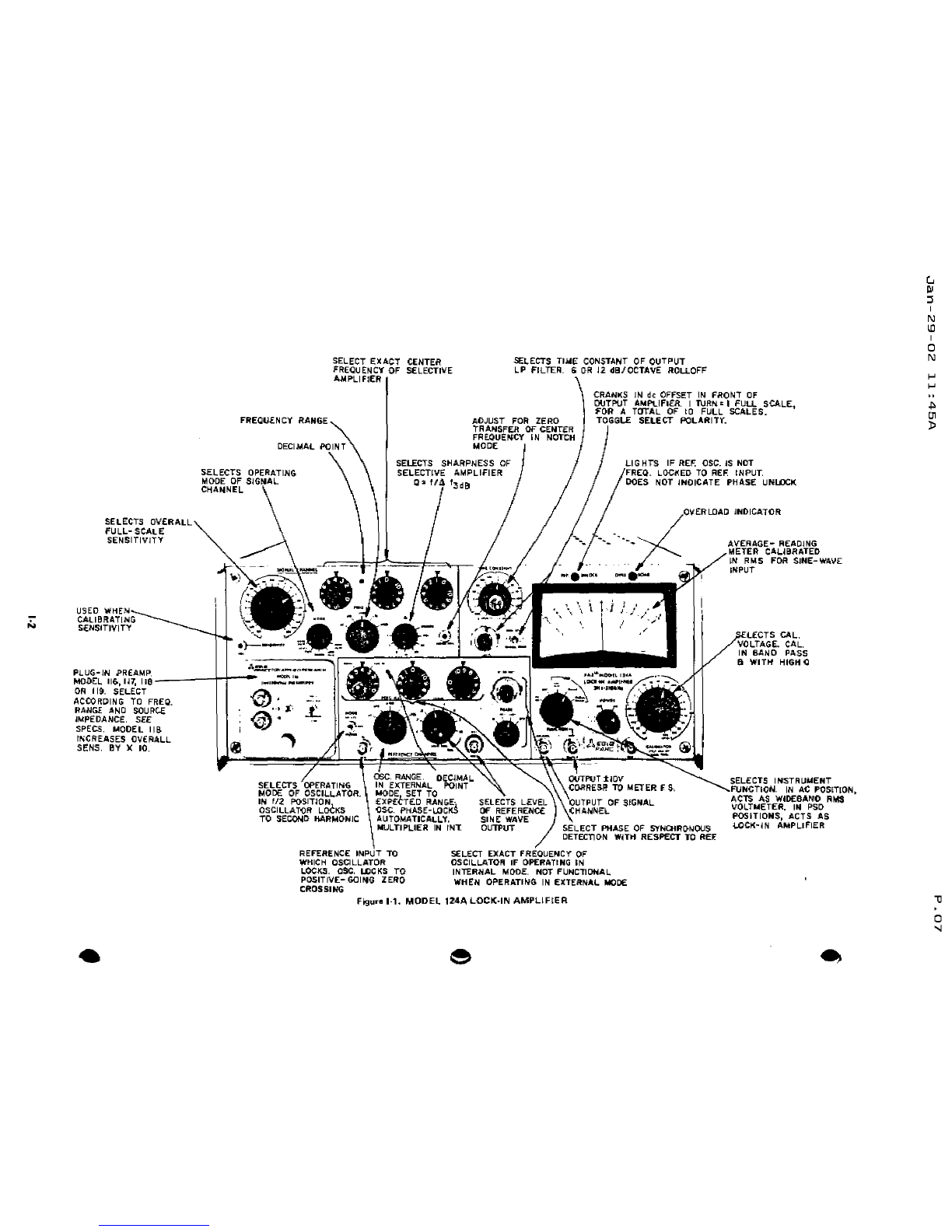
3.1
BLOCK
DIAGRAM
DISCUSSION
3_lA
INTRODUCTION
Bef()r~
discussing
the
actual
operation
of
the
Model 17.4A,
let us e'l;amirll:! a
functional
block
diagram
to
bette
r
understand
what
each
adjustment
does,
and
how
the
various
adjustments
relate
to or
influence
one
another.
The
functional
block
diagram
i$
IQc.:';H~d
on
the
following
page.
Schematics
and
a
chassis
wiring
diagram
ere
included
at
the
back. of
this
manual.
The
Synchronous
Detector
is
the
heart
of
the
instrument.
around
which
are
situated
the
Signal
Channel,
the
Refer-
ence
Channel.
and
the
Output
Amplifier.
The
Signal
Ch
annal
amplifies
and
filters
the
siqnal,
clnaning
it
uo
as
much
as possible
before
passing it
along
'0
the
Synchronous
Detector.
The
Referel1ce Ch(i"r'Iel
controls
svnchronization.
3.16
SIGNAL
CHANNEL
Preampljfle
r
Four
models
of
plug-in
preamplifier'
arc available:
the
Model
116,
the
Model
117,
the
Model
118,
and
the
Model
119~_
Together
they
cover
the
whole
frequency
spectrum
from
near
de
to
210
kHz,
each
model
having
the
best kind
of
input
circuit
for
optimum
tow-noise
performance
in its
frequency
range_
The
Mndel
116
may
be
considerec
the
qeneral-purpose
choice,
performing
well in
most
situations.
Specific
data
for
the
four
preamplifier
models
Is given in
the
specifications
in
Section
I
and
in
the
discussions
in
Subsection
3_1.
Selective
Amplifier
The
Selective
Amplifier
functions
as a variable 0filter,
which
l"Iiay
be
operated
in
the
high-pass. low-pass,
notch,
bandpass,
or
flat
mode.
Because
rrns
noise
amplitude
is.
a
direct
function
of
bandwidth.
much
of
thl!:
noise
can
be
rejected
in this.
stage
by
filtering
out
all
but
the
band
cont
aininq
the
wanted
signal. In
addition,
odd
harmonics,
to
which
the
Synchronous
Detector
is sensitive, clin be
eliminated.
Intermediate
Amplifjer
The
Intermediate
Amplifier
provides
additional
gain so
that
the
siqnat-p lus-ncise
applied
to lhe'
Synchronous
Detector
is
as.
large as possible
without
overload.
Presenting
~J
larqe
signal
to
the
Synchronous
Dete
cror
minimi
....
es.
for
agiven
everett
senstrivitv.
the
noise
and
de
drjft
contributed
by
the
Outp
ut
Channel.
"AI!;!;)
avaIlable
cr e
the
Mod~1
184
Photorn~trjc
Preampldler
Il
....d
the
Morlel
1135
Sirlgle·Erldec1
Low
Nctee
PreamplIfier.
The:~e
two
preampl,f,e(!
ware
devlllioped
laul:(
m
an
the
prU;:IrnlJllflers
dj!lt:U5S~d
in
thl!>
manual.
FOr
infcrm,UIOn
I!Ij~d
slJtlcific",tionl;',
contact
the
factory.
Seoarare
instruc:tion
m811UI!IIIs
lire
prQvidet;l
for
the
Models
184
and
185.
111·1
The
Intermediate
Amplifier
is ac
coupled,
thereby
eliminat-
ing
de
drift
problems
in
the
Signal
Channel.
3.1C REFERENCE
CHANNEL
Voltage-ContrOlled
Osclllator
The
VCO
either
locks
onto
a
svnchronizinq
signal
from
the
e)(periment,
Or
provides
iii:
$Vf'lchroniling signal
to
the
experfrnent.
The
Vee
drives
the
Syr,dlfonOllS
Detector
so
that
the
e
xpertment
an(1
the
Model
124A
are
properly
synchronized.
The
VCO
automatically
phase-locks
to any
kind
of
refer-
ence
waveform
hoving a
frequency
within
approximately
two
decades
of
the Hcfe rcnce
Channel
band
setting.
the
only
requirements
heing
that
the
waveform
cross
the
mean
twice
{onlyI
each
cycle,
that
it
have
apk-pk
amplitude
of
at
least
100
mV,
and
that
it be
svnchroriized
with
the
signal
of
interest.
The
vee
can also
lock
to
the
secono
harmonic
of
the
reference
~ign,al,
if
desired.
I~
is
important
to
realize
that,
even
though
the
VCO
will
phase
lock
over
a
two
decade
frequency
range, the
boundaries
of
the
lwu
dur.ades
an~
determined
by
the
setting
of
the
O~r:iIlMnr
Ranqc
switch.
The
tracking
range
corr
e
spondtoq
to
each
po si
tion
of
the
switch
is as follows.
Xl
,.""".""
_. _
..
__ .
0.2
H,
to
21 Hr
XlO
,.",.""".,,_,
.
2Hlto21OHI
X100
,,,,
.'
__ . _.
..
_
20
Hz
to
2_1 kHz
X1K
"",,
.
._.
200Hz!o21
kHz
XlOK
,
..
, , 2
kHz
to
210
kHz
In the
Internal
mode.
asinewavc OLltPut
from
th~
Oscillator
is
provided
for
synchronizing
the
experiment.
The
Oscil-
lator
can
free
run
accurately
at
any
selecled
frcqvency
from
200
mj-iz
to
210
kHz,
Also,
the
Oscillator's
frequency
may
be
controlled
by a
voltage
applied
to a rear-pane!
jack.
Phase
Controls
The
Phase
Controls
combine
quadrature
outputs
from
the
VCO
such
that
the
resultant
sinewavs
presented
to the
Svnchronous
Detector' has
the
desired
phase
relation
to
the
reference
(sync
input
and/or
output).
3.10
SYNCHRONOUS DETECTOR
The
Svnchronous
Detector
inverts
the
polarity
of
the
part
of
II"Ie
input
signal
ccr
respondinq
to
the naqativc
excursion
of
the
phosc.stutted
sinewave
from
the
VCO.
and
passes
the
remaining
waveform
uninverted.
Therefore,
the
de
corn-
ponent
of
the
resultant
waveform
is
proportional
to
the
value
of
signal at
the
same
frequencv
and
phase
as
the
phase-shifted
veo
sinewave.
Because
the
detected
signal
still has
noise
on
it. RC
low-pass
filters
that
follow
the
svnchrooous
detector
are
used
to
eliminate
ull
but
the
de
component
rspresentinq
the
wanted
signal. A
de
ampllfier
SIGNAL
CHANNEL.
./
A
......
~,
t,
III
:lI
W
o
I
o
N
o
U1
..
N
.J>
il
on
1.'
r-,
M
'1-'
-T
'-~"J
l-·~
,
r---------------T.......,
..
'"J
C\
=0'
~
'0''''
Sc..++
uK-\
TE-5J
-...;..,
I
).)
"
.tJ
)
I
F
0_
o-£T£
CJ1JiII
,..'-0;
.;...l..I'
.(.
.J.~l
:l(
.t' r,
,
•
<t
·0
'j
,
I
,
<"l
~
,".
or
~
I,.-;,•
.t.
>l
1 \
~
r
\ i l·t
..
~
J
I.
I
.'
:u
."
'.
r .
~,
.
.0:..0
,,
~
-
,':,'1
''-1
L'
!.
S"fN(. SINE
....
IE
oolFvr
..-
100
tl
(
I.e'
CALIEllIiU.TOJI
SQU,loJIIIE
'III"VI[
!ion
-=
-=
O('ECro-R
'>
,IG)
~~Pvl
SYNC DRI'o'f1l'
"PII,D
,nKNuAlCfr
CALII!IRaTOR' .[lIIlr¥lEiII
UII~
''IT£No
...rOA
--L.E:'o'EL
"'CAL_
L.[vtL
,
r;:.
""
(-' Or
~
.•
",
JV·' ,
A·Y
D..'-'
" . 'I.' "
:_"'~
tI,.,.r
."\
\
\ ..
X'
',i
j
~
..eli"
o'
,
,
--TIME: CONSTANT
,/
"l"(II(I
WF'PAESS
""./"
"'.....
"'7
,,
.
-l-:-'-
~~;;~t-
--
-
--
--
-
-----
.
~
. v ...
J
-~."
...
.t;
FIJ"ICTION"'/
.".
- i1'" F'HA5£
.-----.
<a<ll<1S
.2JO"
-
..
OO(
..
.J"FI!EOJ;[IIIC"f
.....
.[F.
lJI'Il.OClI;
II'I00oC-ILTOiII
VOLTAGE
-<:OHIAOLL.ED
f'ootI,I,S(-L-D::lIlo[O
OSCILL"TQIll
• ...ODI::
..
f"I'IEQUEP,!C
....
'0
:S~NC
"'OUT
,"tl
l
r
<,
<,
-i
~
~SOI~;IY1
v1
T"
.............
.............
iREFER£NeE
CMANNEL
•
....
ODE~
IHi
..
QI' I
It
".po I 18 IX or
1"1)r[1'!I
..
INOl'CATES
FRON
r
,....NEl. COtITROL
Sl~"
"","IS
=
N
...
Fig""
III~'.
FUNCTJONAL
BLOCK
OIAGRAM.
MODEL
t24A
-
~
,I.'I
,
,.;
il
>
o
'"

Jan-30-02
05:24P
P.02
following
the
Detector
provides
the
finesl
gain.
This
ampli-
fier drives
the
output
connector
and
panel
meter.
To
daterminu
the
amplitude
of
asignal.
the
operator
simply
adjusts
the
phase
controls
for
maximum
meter
indication.
The
meter
directly
indicates
the
signal
amplitude.
In
addition,
after
making
thil
adjustment.
the
phase
of
the
input signal relative to the reference may be accur etelv
r~ao
from
the
Phase
dial.
3.2
SIGNAL
CHANNEL
OPERATION
3.2A
INTROOUCTION
The
function
of
each
control
is
indicated
in
Figure
1-1.
Instead
of
repeating
the
intormatlcn
qiven
there,
this
subsection
provides
additional
background
information
for
setting
the
controls
to
their
optimum
positions.
To
set
I,JP
the
Signal
Channel
controls,
the
operator
rnusr
know the
frequency
or
frequency
range
of
the
signal. It also
halps if he
knows
the
expected
amplitude,
the
amount
and
tvpe
of
noise
obscuring
the
signal. and
the
signal-source
impedance.
The
stimulus
to
the
e
xpsrirne
nt is
often
chopped,
Detecting
at
this
chopping
freqi
...
encv
eliminates
all
but
the
signal
related
to
the
stimu
Ius.
Princeton
Applied
Research
Corpo-
ration
manufactures
several
models
of
light
chopper
which
are ideallv
suited
to
photo-detection
applications.
Chopping
the
source
light
finds
its
analog
for
other
kinds
Of
experiments
in
chopping
the
stimulus
de.
ri, ac,
sound,
heat,
etc.
The
chopninq
frequency
range
must
be fairly well
known,
and
sync
sigr\als
must
be aViJilable. Of
course,
the
frequency
of
interest
may
not
be a result
of
chopping
at all.
The:
chopping
technique
discussed
here
merely
serves as an
exampl
•.
3.28
PREAMPLIFIER
CHOICE
Four
models
of
plug-in
ureampltflers
are available.
each
one
providing
optimum
low-noise
performance
over
a given
input-resistance
v,
frequency
ranqe, as
shown
graphically
in
Figure
111-2.
Two
of
these
preamolifiars
can be
operated
both
in
direct
and
transformer-coupled
modes,
and
all
four
of
them
can be
operated
single.ended
or
differentf
allv, A
Model
190
transformer
can
be
used
with
any
of
the
plug·ins
to
improve
low-frequency
performance when working
from
low
source
impedances.
Use
of
the
Noise
Figure
contours
is
discussed in
Subsection
3_2G.
Another
consideration
in selecting a
preamplifier
is its
ability
to
amplify
without
distortion.
If an
experiment
requires
measurement
of
low
level
harmonics
in
the
presence of ahigh level Iundarnentat, it is
important
that
tho
preamplifier
not
add
significant
harmonic
signals by
non-linearly
amplifying
the
fundamental.
Except
in
the
case
of
the
Model 118
Preamplifier,
the
distortion
generated
by
preamplifiers
operating
in
the
direct
mode
is so small as
to
be
unmeasurable
using
conventional
methods.
The
Model
11B
tan,
however,
distort
more
und~r
certain
conditions,
as
indicated
in
Figure
111-3. In
the
transformer
Mode,
both
phase
shif~
and
distortion
must
be
measured
for
each
individual
operating
condition.
Figure
111-3.
DISTORTION
v.
FREQUENCY.
MooEL
118
zo "'v
10'
10.11
10"
,R!QuENCV.
Hz
I;URY!$
1111142:
APPLY' FQR
ALL
MODEL
1Z~
$~SITlVITY-p$(J
SETTING
COJolelNATIONS EX"CEPT:
p:Sc_
LO
DR,
SEN
~
10
~V
UHl,i
-'00
",Vi
f1'S D &
NO~MAl,
SEN
~
1 roY
Ihrll
W
'00
e v ; j!I!iD _I'll DYN RNIJ, $£N ..
l00
pY
",,"
"'00
1ft 1/. :;.
"OR
il'1ESf
COM~INATION:S,
CURlifS
~o1l1;!4
APPL....
II
100
roY
":.;
10 "'v
~~
~
..
'::~
J~
e
ev
i!a.
~I
~1
~~
;;:i
tnt;;
~t.
10
3.2C
GROUNDING
In any
system
processing
low-level signals,
proper
grounding
to
minimize
the
effects
of
ground-loop
currents,
usually
at
the
power
frequency.
is an
important
consideration.
With
the
exception
of
the
Models
184
and
185,
all
of
the
Model
124A
preamplifiers
allow
both
differential
ar\d
single-ended
opaearion.
Two
properties
of
these
nraamofitiers
allow
them
to achieve a
high
degree
of
immunity
to qround-f
onp
currents.
In
differential
operation,
their
extremely
high
ccrnmon-rncde
rejection
(:l.SSUI'es
an
almost
t
otal
rejection
of
'.0
;!.
~.
Q
;:
"
-I
Q
10
t;
Ci
110
..
10
10
JQJ
'lOt
I'''EQUI!NCY. HI
11$,
II
",
..
119---"
tllll'Eer
IIIQfI[
101.0
Fig!,.....
111.2'.
OPTIMUM
PERFORMANCE
REGIONS
OF THE PREAMPLIFIERS
10
'0
10'
'0'
10'
~
~
10'
10'
111-3
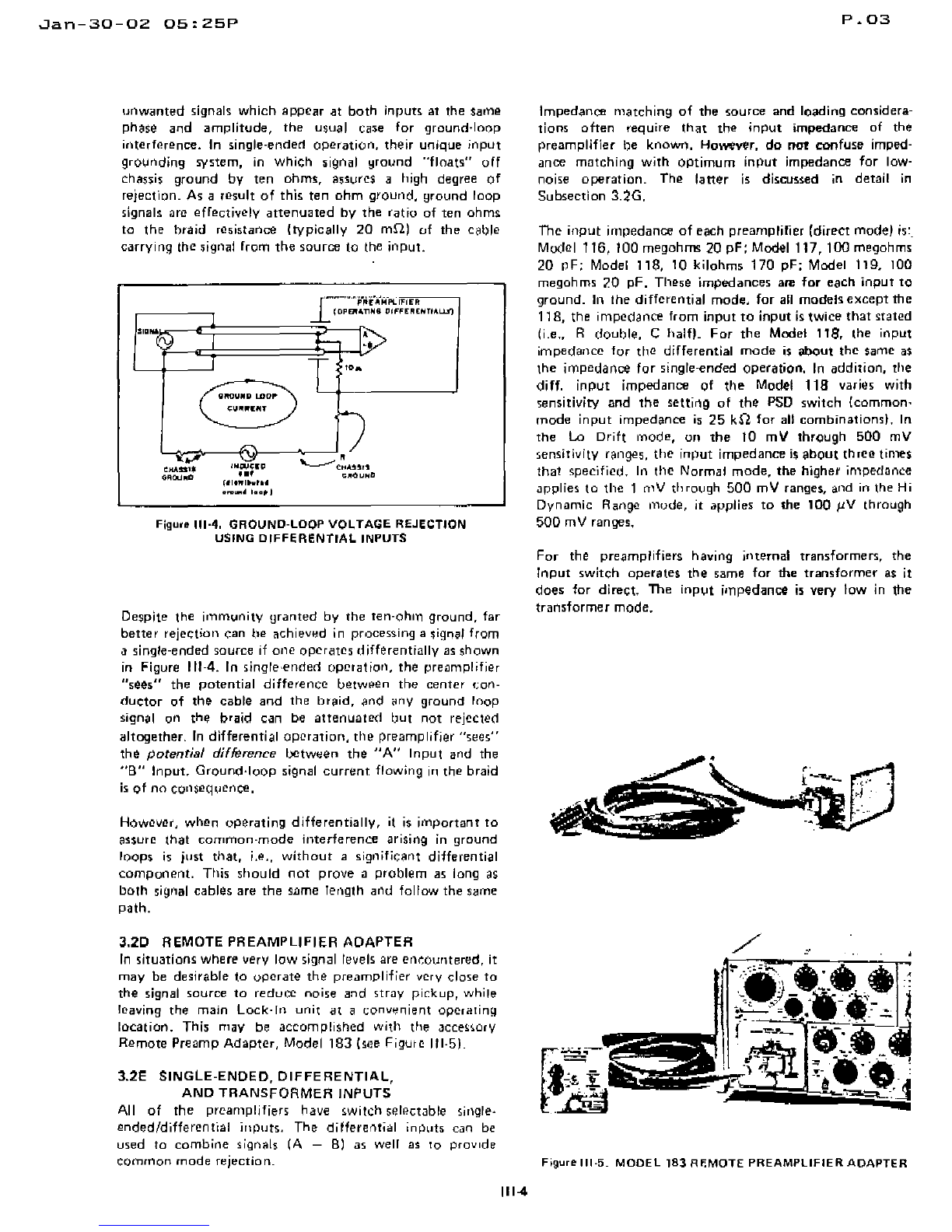
Jan-30-02
05:25P
P.03
Impedance
matching
of
the
source
and
loading
considera-
tions
often
require
that
the
input
impedance
of
the
preamplifier
be
known,
HOMVer.
do
nat
confuse
imped-
ance
matching
with
optimum
input
impedance
for
low-
noise
operanon.
The
latter
is discussed in
detail
in
Subsection 3.2G.
The
input
impedance
at
each
preamplifier
(direCt
model
is:.
Mo<:fel
116,100
rneqohrrs
20
pF;
Model
117,
100
msqohms
20
pF;
Model 118, 10
kilohm'
170
pF;
Model 119. 100
megohms
7.0
pF.
These
impedances
are
for
each
input
to
ground.
In
the
differential
mode.
for
all
models
except
the
118,
the
impedance
from
input
to
input
is
twice
that
stated
(;.e., R
double,
C
heltl.
For
the
Mod.1 118, the
input
impedance
for
the
differential
mode
is
about
the
Same as
the
jrnpeuance
for
single-ended
operation.
In
addition,
the
ditt.
input
impedance
at
tile Model
118
varies
with
sensitivity
and
the
setting
of
the
PSD
switch
Icomrnon-
mode
input
impedance
is
25
kO
for
all
combtnattcns
l. In
the
Lo
Dr;ft
mode, on
the
10
mV
through
500
mV
sensirlvltv ranges,
the
input
impedance
is
about
threa
times
that
specified.
In
tIH!'
Normal
mode.
the
higher
impedance
applies
to
the
1 (nV th rouqh
500
mV ranges,
and
in the Hi
Dynamic
Range
mude,
it
applies
to
the
100
IlV
through
500
mV ranges,
•
.,
Figu,01ll·4, GROUND-LOOP VOLTAGE REJECTION
USING
DIFFERENTIAL
INPUTS
GI'OUIUI LDOI'"
I;UIIlIII'
Jan-30-02
OS:2SP
P.04
If an
external
transformer,
SI,H;h
~$
the
Model
HJO, is
used.
it is
connected
to
the
preamplifier
single
ended.
The
ansf'orrncr
alone
provides
sufficient
common-mode
r@jec-
lion
l~igure
III-Eil.
The
total
output
noise
rnav
be
converted
to
an
equivalent
input
noise
by
dividing
by
the
amplifier
gain_
The
noise
figure,
expressed
in
these
terms,
becomes:
(2) Noise Figure =
2010
total
rms
nois_~."'O!,;)gC'
referred
.~~.an1p.
input
dB
IJ10
source
thermal
noise
voHaqe frrl'ld
source
(3)
Total
equivalent
rrns input noise
voltage
thermal
noise"
antilog
NF/20
volts
rms.
Using
the
applicable
set
of
contours,
the
total
equivalent
rms
input
noise can be
de
terrnined:
E=
V4KTBR
Each
amplifier
has its
own
characteristic
noise
figure.
which
varies as a
function
of
frequency
and
source
resistance.
These figures
are
obtained
e
xperimentatlv
and
plotted
graphically.
Figure,
111-7
through
111-11
include
typical
sets
of
noise figure
contours
for
the
Models
116,
117.
118.
and
119
operating
in
direct
and
transformer
modes.
Althnuqh
the discussion
of
noise
considerations
is
not
eomplcte,
a
simple
example
at
this
point
illustrates
the
use
of
the
Ioreqoing
equations
and
illustrates
how
a
transformer
can,
on
occasion,
improve
the
siqnal-to-notse
ratio:
Notice
from
these
equations
that
the
bandwidth
must
be
specified:
usually
determined
by
the
external
circuitry
and/or
the
amp
lifisr
bandwidth.
Figure,
111-7
through
111·11
include
response
curves
of
the
preamplifiers
from
which
the
bandwidth
may
be
obtained
(in
the
direct
modes,
the
bandwidth
is
wider
than
the
widest
Tuned
Amplifier
Bandwidth).
However,
a
more
interesting
place
to
deter-
mine
noise level is at the
output
of
the
Tuned
Amplifier.
Because
there
is gain
ahead
of
the
Tuned
Amplifier.
its
noise
contribution
referred
to
the
input
is negligible
compared
to
that
of
the
preamplifier.
In
computing
the
total
equivalent
input
noise
of
the
signal
channel,
the
operator
only
need
use a Af as
determined
by
the
Selective
Amplifier
sattinq
(with
preamplifier
limitations
considered).
Suppose
that
one
intended
to
operate
the
Model
124A
in
an
experiment
havirig a
source
impedance
of
10
ohms.
Further
suppose
tho
signal
frequency
to
be 5 kl-lz, A Model
116 Prp.arnplifip.r is
chosen,
In
order
to
see
how
a
transformer
car"!
improve
low-noise
performance,
the
noise
for
the
Direct
mode
is first
calculated.
Then
the
noise for
trans-former
operation
is
calculated
and
the
results
com-
pared. Since
the
source
thermal
noise
contributing
to
the
total
noise is
dependent
on
bandwidth.
the
Signal
Channel
bandwidth
is
minimized
by
setting
the
Mode
switch
in
the
Bandpass
position
and
the
0
switch
to
the
10% ENBW
(equivalent
noise
bandwidth!
posf
non,
The
Freque-ncy
controls
are
set
to 5
kHz.
In
addition.
other
control
settings
are
made
ac:con.fing
to
instructions
in
other
parts
of
this
section.
The
source
thermal
noise
in
this
case
is:
where:
k is
Boltzmann's
constant
=
1.38
xHr
iJ
ioules/K
~.
~
,
!
n.
I
Ii •
~oo'
,
<i"'IQ
-,
I".
Go,n
'"
f.~I.
)'<,
Ill !!
eoecr.
117,
II
'I!II
(ll1iI'(cr
,
i
.0
~----L.-----
.L.------.L------"..L-...LL
'0
!l}~
10 1
F~fOU[NCY,
HI
ee
I---------.j---
z
o
"
U
Ita
~
•
z
-
c
c
•
,
is
100
f--,L---+-
•
z
c
"
3.2G
NOISE
AND
SOURCE
RESISTANCE
Best preamplifier performance is realized under
thost;!
conditions
where
the
overall
signal-to-noise
ratio
is least
oeq-aoeo.
In
many
instances.
the
thermal
noise
generat~d
by
the
signal
source
resistance
is
the
dominant
factor
in
determining
the
input
signal-to-noise
ratio.
In this.
respect.
amplifier
noise
performance
can be
specified
by
the
amount
of
noise
the
amplifier
adds
to
the
amplified
source
thermal
noise;
expreS5~O
ira
decibels this is
called
the
"Noise
Figure";
20 109 10
tO~()t
rn)~
nUI$e
"'~~~~_e.":I.~I,hE::
'~,~T,l,P~.fi~,L.~.L.:!~
dB
gain x
source
thermal
noise
voltage
(mlsl
where
the
Source
Thermal
Noise =
-J
4K
lR~f
volrs
rms
~
E,
and
(1) Noise Figure =
Figur.III·6. TYPICAl COMMON·MOOe REJECTION
K=
Boltzmann's
constant,
l.J8
x
10-
2J
joules/K
T""
absolute
temperature
in
kelvins
.1.f
l1'li
equivalent
noise
bandwidth
in Hz
R=
source
resistance
in
ohms
3.2F
COMMON·MOOE
REJECTION
Figure
111-6
illustrates
the
common-mode
rejection
charac-
teristics
of
the
preamplifiers. in
both
{differential)
direct
and
transformer
mode
operation.
Note
that
the
CMR Is
much
higher
for
the
transformer
mode
than
for
the
direct
mode.
•
,
111-5
Jan-30-02
05:25P
Tis
the
absolute
temperature
of
the
source
in kelvins,
presumed
to
be
290
K
for
the
example
Bis
the
noise
bandwidth.
'""
500
Hz
with
a
switch
set
to
10%
ENBW
and
Frequency
Controls
set
to
!;i
kHz
Ris
the
source
resistance
in
ohms,
given as 10
ohms,
ThuS'E
=y'4
x1.38 x
iiJ-
BX
2.9
x
1'0'
x
TO
x
5~
10"
-;
8.9 XTO-? V
rms
From
Figure
111-7.
the
noise figure
for
the
Model 116 at a
center
frequency
of
5
kHz
and
a
source
impedance
of 10
ohms
is
20
dB.
Substituting
E
and
this
NF
into
equation
131.
we
get:
total
equivalent
rrns
input
noise
=
8.9
x
10-'
x10
'0,'0
=89nVrms
With a
transformer
inserted
between
the
signal
source
and
the
amptificr
input
we
can
increase
the
effective
source
impedance
to
a
value
that
reduces
the
noise
figure to less
than
0.1
dB.
From
Figure
111-7,
the
source
resistance
should
be
about
200
kilohms.
The
transformer
turns
ratio
required
for
this
ilTlpt.:!dance
tncrease
is
yR~IR~
=141. TIle
thermal
source
noise
at
the
amplifier
i
nput
is
equal
to
the
noise
generated
by
the
10
ohm
SOL;rcC
multiplied
by
the
turns
ratio.
With
a
noise
figure
near
zero,
thl~
total
equivalent rms
input
noise
is
also
equal
to
the
noise
generated
by
th!1
10
ohm
source
multiplied
by
the
turns
ratio.
z.
1.25
J1V
rrns.
I\lthough
the
numerical
value
of
equivalent
input
noise
is
much
larger
than
before,
the
signal-to-noise
ratio
is sub-
stentiullv
increased.
This
can
be
seen
by
coruiderinq
all
of
the
transformed
source
!iignal
voltage
as
appearing
at
the
amplifier'
input
terminals,
p05sibla
because
the
Model
116'5
input
resistance
is
much
larger
than
200
kilohms
presented
by
the
transformer;
the
siqnal-to-noise
ratio
is
equal
to
the
maximum
possible
value;
esig/(E
x
antilog
NF/20)
=?.
esig/E,
the
norse
contributed
by
the
amplj Her
being
negligible
under
the
"near
r
ere"
noise
fiqure
conditions.
In
this
example
the
transformer
ifl(rr.aSf~S
the
slqnal-to-noise
ratio
by a
factor
of
TO.
Signal·to,Noise
Improvement
Ratio
TOINF
unmatched
-
NF
matchedl/20
TO
(20
--
-
11/20
~
10 '=10
However,
because
of
the
noise
contributed
hy
the
trans-
former,
and
because
a
transformer
influences.
bandwidth,
the
results
obt
ained
using
3real
trensformer
are
never
as
good
<:15
the
ideal
theoretical
resul
ts
predicted
in
the
example,
Also,
it
is
seldom
convenient
to
obtain
a
tr
ansfor
me r
having
cxectlv
the
ideal
hHn5
ratio.
It is
best,
therefore,
to use
noise
figure
contours
and
amplitude
tr
ansfer
curves
obtained
ernpiricallv
for
th~
individual
transformer.
Figure
1l1·8A is
~
set
of NF
contour's
for
the
111·6
P.05
Model
116's
built-in
transformer.
and
Figure 11I·8B i. its
amplitude
transfer
curves.
The
10·ohm
amplitude
tran$fet
[.:urve
indicates
that
in
this
example
thll!:
transformer
does
not
t;:"han9fi!'
the
10%
equivalent
noise
bandwidth
as
set
with
the
Q
switch.
'0
that
E
remains
8.9 x
llr'
Vrrns. The noise
fjgure
for
a
10
ohm
source
at
acenter
frequency
of
5
kHz
is
about
1.5 dB, aVast
improvement
over
the
20 dB NF
obtained
without
the
transformer.
NOTE:
For
optimum
noise
performance
with
atrans-
former,
it is
important
that
the
transformer
not
be
magnetized.
See
rRANSFORMER
MAGNETIZATION
ANO
DEGAUSSING,
page
111-'
r.
3.2H
SELECTIVE
AMPLIFIER
Noise
other
than
Source
thermal
noise
is
usuallv
not
wideband,
and
is
often
difficult
to
compute.
Some
kinds of
noise
can
be
dealt
with
very
effectively
u$ir~9
the
Selective
Amplifier.
Examples
include
flicker
(or
1If)
noise.
non-
synchronous
signals
arising
from
the
experiment,
non~
svnchronous
$igrlals.
from
external
pickup
such
as
from
the
sc
power
lin~.
fast
transients,
and
harmonics
of the
reference
frequency_
Reducing
the
noise
level
ahead
of
the
mixer
reduces the
dynamic
range
demand,
on
the
mixer.
tllereby
allowi~9
signals
to
00
measured
which
could
not
be
measured
otherwise.
The
Selective
Amplifier
can
be
operated
in five
dillerent
modes:
Flat.
flandpass,
Notch.
Low Pass,
and
High Pass.
Figures:
111·14
through
111-17
lltustrata
typical
transfer
characte
nsrtcs
of
the
Selective
Amplifj@r for
the
last
four
of
these
modes,
Ultimate
attenuation
of
the
four
frequency-
dependent
curves
exceed
80
dB.
In
selecting
filtering
per
ame
ters,
the
operator
must
be
careful
to
keep
the
signal
frequency
well
within
(he
passband selected, or
to
make
the
passband
such as to
accommodate
the
sigrlal
over
th~
range
that
it will
occupv.
If
chase
i$
important,
actual
measurements
of
phase
error
over
the
frequency
range
of
questionable
phasu
accuracv
would
be
best.
These
regions
of
questionable
C1ccuracY
can
be
determined
from
the
individual
transfer
characteristics
of
the
preamplifier,
transformer,
and
Selective
Amplifier
settings.
The
bes
tthinq
to
do
is
to
keep
the
bandwidth
wide
enough
so
that
phase
and
amplitude
errors
ars
not
a
problem.
Phase
control
errors
are discussed in Subsection
3.38.
Special
procedures
for
making
accurate
phase mea-
surements
are given in
Subsection
3_9. In
particular,
before
oper
atin
qin
LOW
PASS
or
HIGH
PASS,
the
operator
is
advised
to
check
Figures
111-16
and
111-17
to
determine
the
amp!
itude
responses
in
these
modes
as a
function
of
Q_
"Equivalent
noise
bandwidth"
is a
concept
applied
to
widebano
noise.
Although
most
bothersome
noise
is
not
wideband,
but
rather.
coherent
non-synchronous
signal,
equivalent
noise
bandwidth
considaratfons
are usefu! in
helPing
to
choose
operating
parameters.
The
concept
of
«quivale
nt
noise
bandwld
th
arises
from
the
fact
that
Noise
Bandwidth
is an
unartenueted
rectangular'
bandwidth,
while
(cont.nued
on
page
111-131
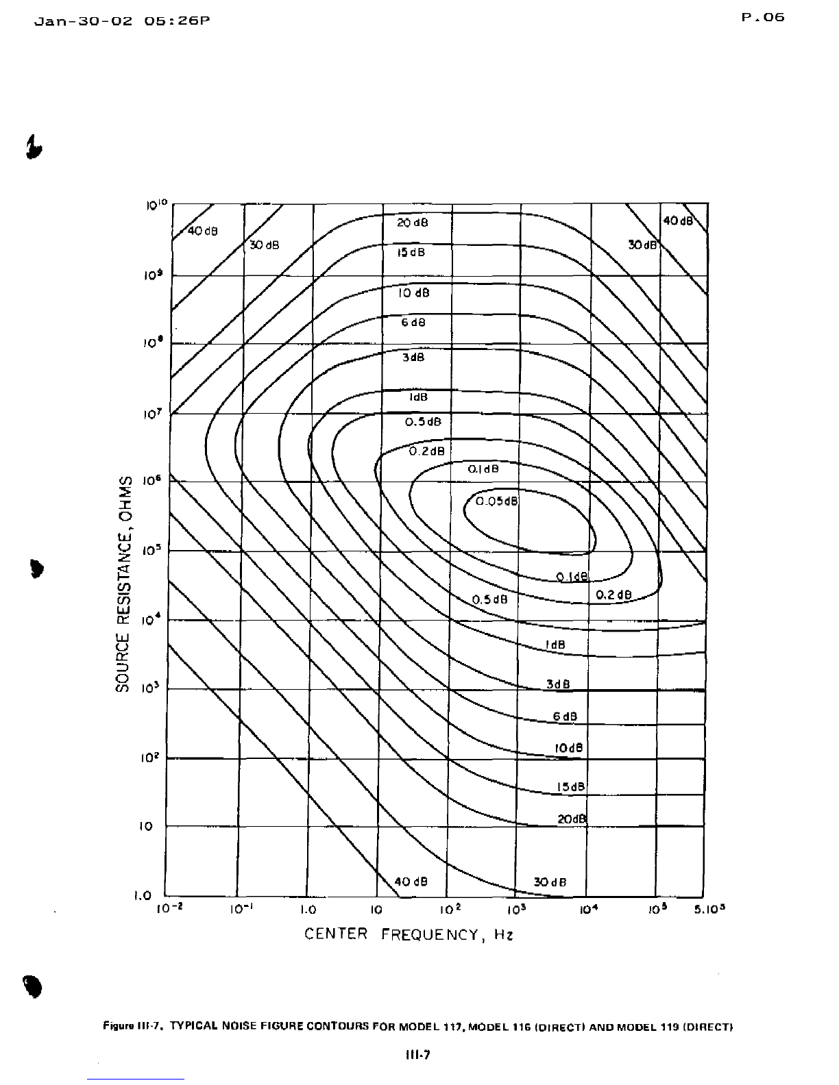
Jan-30-02
05:26P
P.06
5.10'
10'
!OdB
101.0
10"
1.0
10-'
10'0
20dB
15dB
lOt
10 dB
6dB
10'
3dB
IdB
10'
0.5dB
o.ras
If)
10'
:=!
::r:
0
w
V
10'
Z
~
en
en
I.lJ
10·
0::
I.lJ IdB
U
0::
::l
0
10~
3dB
(f)
BdS
lOde
10'
15de
20d
10
CENTER
FREQUENCY
IHz
Fit.rolll-?
TYPICAL NOISE
FIGUIIE
CONTOURS
FOil
MOOEL
111.
MODEL
11G
IDIIIECTI
AND MODEL
119
(D1I1ECTI
111·7

Jan-30-02
OS:27P
P.07
EO,"
IE
I~
(TURNS
RATIO
I:
100)
>-
u
Z
on'"
::>
o
'"
'"
LL
N
a
...
o
..
o
-
o
o0 0 0 0 0 0 0 0 0
0-
I"'1N
...
am
co
p....
to
III
'"
""
_,
--
--
~
<,
x
-, ,"
~
--
""
,,'
I
,.
I·
·•
,•
,
I\\·•
·
\•..
II·\\
·•,
II·
·
·
·
Wwwl.LJ
\
(,)uuu
\
0:0::0::0:::
:::>::J::J:::J \
0000
V)
(I)
(1)(1)
c:c:c:c:
,
-000
-00
"
-on
I~
10·
101
10'
({)
:::;;
:r
0
w102
0
Z
~
IdB
(()
iii 10
W
a:::
~dB
W
U
6dB
a:::
I
~
I
-----+-
01.0 - I
U)
10dB
;
I
15dB:
10-'
zo
aa
I1
Ii
10-2
3~--
-:=--T
I
i
10-'
II
1.0 10 102
10'
104
CENTER FREOUENCY,
Hz
Figure
1l1-8A.
1VPICAL
NOiSE
FlGURE
CONTOURS
~OR
MODEL
116
OPERATING
IN
THe
TRANSFORMER
MODE
Figur~
111-8B. TYPICAL
AMPllrUDE
TRANSFEA
CURVES
FOR
MODEL
1'6
OPERA
riNG
11\1
THE
TRANSfORMER
MODE
111-8


