Ptek FM Series User manual

HANDBOOK
BROADCAST FM EXCITERS
FM SERIES
PTEK

Limited Warranty
PTEK (SELLER) warrants that products are free from defects in material and workmanship and meet
p
erformance specifications provided, however, that:
(A) SELLER’ liability under this Warranty is limited to repairing or replacing, at its option, any
product delivered here under not conforming to this Warranty;
(B) This Warranty is limited to a period of two years;
(C) Minor deviations from specifications which do not affect performance are excluded from this
Warranty; and
(D) SELLER shall be liable under this Warranty only if:
(1) It is promptly notified in writing by the Buyer upon discovery of the failure of any product to
conform to this Warranty,
(2) The product is returned to SELLER, transportation charges prepaid by the Buyer,
(3) The product is received by SELLER not later than ten days after the last day of the one-year
period of this Warranty, and
(4) SELLER’ examination of the Product discloses to SELLER’S reasonable satisfaction that
such defects or failures as may exist have not been caused by misuse, neglect, improper
installation, repair, alteration, accident or shipping.
The Buyer will prepay freight to and from SELLER on products serviced here under at SELLER’ plant; but
SELLER may, at its option, elect to perform any repairs here under at the Buyer’s place of business.
The foregoing constitutes SELLER’S entire Warranty expressed, implied and/or statutory, except as to
title, and states the full extent of SELLER’S liability to the Buyer or to any other party for any breach of
such Warranty and for damages, whether direct, special, incidental or consequential; and, other than as
expressly provided in this document. No Warranties, expressed or implied, including any Warranty or
merchant ability or of fitness for a particular purpose, are made. No employee, representative or agent of
SELLER has any authority, expressed or implied, to alter or to supplement the terms of this Warranty.
Warranty Service
The Limited Warranty covers parts and labor to the original purchaser for one year. Damage
caused by misuse or shipping is excluded from the warranty. Before returning units or material,
contact the factory for a Returned Material Authorization (RMA) number. Ship all materia
l
prepaid. Defective material should be addressed to:
PTEK
Customer Service Manager
1814 Schooldale Drive
San Jose, CA. 95124
(408) 448-3342

Page 3
Contents
Safety Notice .................................................................................................................4
Rear
FCC, Accessory Connections & efficiency V O/P Pwr.................................................12
Schematic Chassis FM150E...................................................................................16-17
Schematic Power Module FM150E..............................................................................20
Schematic Power Module Control FM150E.................................................................21
Parts list Chassis...........................................................................................................22
Parts list PA Boards......................................................................................................23
Parts list Synth Board ..................................................................................................25
Parts list LED Board ....................................................................................................25
Specifications ................................................................................................................5
Front & Panel Layout .............................................................................................6
Installation .....................................................................................................................8
Schematic Synthesizer ...........................................................................................12-13
Schematic Chassis ..................................................................................................16-17
Schematic Power Module ......................................................................................18-19
PROVISIONAL......................11/25/96
REV A.....................................1/16/97
REV B.....................................10/7/97
REV C.....................................4/13/99
REV D.....................................5/24/99
Rev record

Safety
BEFORE APPLYING POWER
GROUND THE EXCITOR.
Fuses
.
DO NOT OPERATE IN AN EXPLOSIVE ATMOSPHERE
DO NOT REMOVE THE EXCITOR COVER
Output connector
Verify that the line voltage is 115V
To minimize shock hazard, the excitor chassis must be connected to an electrical ground. the excitor must be
connected to the ac power mains through a three-conductor power cable, with the third wire firmly connected to an
electrical ground (safety ground) at the power outlet. Any interruption of the protective (grounding) conductor or
disconnection of the protective earth terminal will cause a potential shock hazard that could result in personal injury.
If the excitor is to be energized by any other source be certain the that chassis is connected to a separate safety
ground.
Only fuses with the same required current, voltage rating, and specified type (normal blow, time delay, etc.) should be
used. Do not use repaired fuses or short-circuited fuseholders. To do so could cause a shock or fire hazard
Do not operate the power amplifier in the presence of flammable gases or fumes.
Operating personnel must not remove the exciter cover. Component replacement and internal adjustments must be
made only by qualified service personnel.
The type N output connector carries dangerously high RF voltages which present a shock and burn hazard.
operate this excitor with out the out put connector properly terminated in either an adequately rated load or antenna.
NEVER
Page 4

Specifications
MONAURAL
Audio Input Impedance:
Audio Input Level:
Audio Frequency Response:
Total Harmonic Distortion:
FM S/N Ratio (FM Noise):
Asynchronous AM S/N Ratio (AM Noise):
Synchronous AM SIN Ratio (Incidental AM Noise):
600 ohms, balanced
+10 dBm (6.93 volts peak-to-peak) at 600 ohms for
75 kHz deviation
+/-0.5 dB; flat or 75 microsecond pre-emphasis, 20
Hz to 15kHz (other time const. available)
0.15% max.; 20 Hz to 15 kHz
70 dB min. below 75 kHz deviation at 400 Hz,
measured within a 20 Hz to 15 kHz bandwidth with
75 microsecond de-emphasis
60 dB RMS. below carrier; reference: 100% AM
modulation, at 400 Hz with 75 microsecond de-
emphasis, no FM modulation
57 dB below carrier; reference: 100% AM
modulation, full power at 400 Hz with 75uS de-
emphasis, FM +/- 75 kHz, 400Hz
ENVIRONMENT
Altitude: Ambient Temperature
0-10,000 ft -10 to +50 oC
WIDEBAND
Inputs:
Input Level:
Wideband Amplitude Response:
Composite Unbalanced 75 Ohms
SCA 1 Unbalanced 75 Ohms
3.5 V RMS. (10 Volts peak-to-peak) for 75 kHz deviation
+/-0.5 dB, 20 Hz to 100 kHz
GENERAL
Rated Power Output:
Power Consumption:
Frequency Range:
Frequency Control:
Frequency Stability:
Output Impedance:
Output Connector:
VSWR:
Modulation Type:
Modulation Capability:
Multi-Meter Indication:
Harmonic Attenuation:
10W, 25W, 50W, 150W, 300W
750 W (for 300W model)
87.7 to 108 MHz, in 200 kHz steps (other step
size to order)
Phase locked loop frequency synthesis from high
stability master oscillator
+/- 1.2 kHz
50 ohms
Type -"N" female
1.5:1 for full power, derate to 0 at inf.
Direct carrier frequency modulation
Internally limited to 100 kHz deviation
Deviation, Forward Power, Reverse Power, Final
I&V
-70 dB, min.
Page 5

1
4
6
Rear panel layout
876
5
12
34
Page 6
Front panel layout
. DEVIATION
23
8
7
ON
REMOTE
PWR PWR
VOLTAGE
FWD REV
OFF CURRENT
FINAL MONO IN
600 OHMS
AC IN
GAIN
COMPOSITE
GAINGAIN
SCA
FUSE
RF OUTPUT
FINAL CURRENT
FINAL VOLTAGEFORWARD POWER
REVERSE POWER
ADJ
POWER
OFF
OPERATE
REMOTE OFF
FAULT
DRIVE LOW
FM Series
PTEK
FM10E
DEVIATION
30
25
20
15
10
5
OUTPUT POWER W (REV X0.1)
4.0
40
3.0
30
2.0
20
1.0
10
0
0AMPS
PTEK
VOLTS
DEVIATION kHz
100
75
50
25

Key Element Description
1AC IN & FUSE 110 VAC input and Fuse 10A
2COMPOSITE Unbalanced wide band composite input
3SCA Unbalanced wide band input
4RF OUT TYPE N RF Output
5GAIN ADJUSTMENT Composite & wide band level adjustment
6Accessory connector Connections for; Remote off and DC indications of Forward Power, Reverse
Power, Final Voltage, Final Current and Deviation.
7FCC ID Type approval number
8SERIAL NUMBER Serial number for reference purposes
Page 7
Key Element Description
1METER Indicates Forward Power, Reverse Power, Final Voltage, Final Current and
Deviation
2OPERATE Switch and
Indicator
This switch sets the FM Broadcast Amplifier to the Operate Mode; 110 VAC is
applied to the line transformers and this amber indicator is lit.
3REMOTE OFF Indicator This red LED indicator is lit when the FM Broadcast Amplifier remote off
terminals (rear panel) are open circuit.
3DRIVE LOW Indicator This red LED indicator is lit when the FM Broadcast Amplifier can not make the
power requested, because for example low drive power.
5FAULT Indicator This red LED indicator is lit when the FM Broadcast Amplifier is in a fault
condition. This can be for one or combination of the following:-
Over drive, High supply Voltage, High load VSWR, Over temperature.
6 Meter Select Switch This switch selects one of the following to be presented on the meter (1):-
Forward Power, Reverse Power, Final Voltage, Final Current and Deviation.
7ADJ POWER control This control adjust the output power from rated full power to less than 50%.
8 Ventilation Filter This provides for filtering the environmental air as it is drawn into the cabinet by
the internal fan (not used on FM10E).
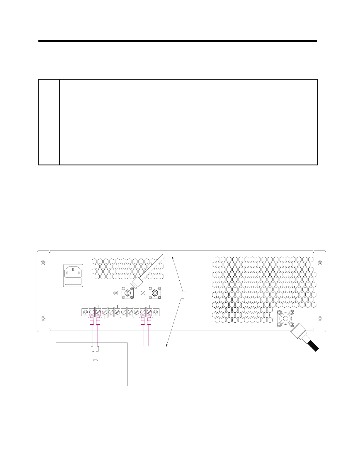
Refer to the Table below for the following description. The installer should assure the ac line voltage is turned OFF
before performing this procedure. The electrical connections are installed at the Exciter rear panel.
Installation-Electrical
Step Procedure
1 Connect the load RF line to RF OUT connector.
3 Connecttheaclinepowertotheaclineinconnector.
4 Optional. Connect the remote site metering, to the rear terminal block.
5 Connect either the composite input to the output from a stereo encoder or the balanced mono input to a
program source
Page 8
AC IN
SCACOMPOSITE
GAINGAIN
600 OHMS
REV
PWRPWR
FWD
CURRENTVOLTAGE
FINAL MONO IN
REMOTE
ON OFF
GAIN
RF OUTPUT
RG8 TO ANTENNA/PA
PART OF USER SUPPLIED REMOTE CONTROL
BALANCED MONO IN
OR (NOT BOTH)
FROM STEREO ENCODER OR STL

Refer to the Table below for the following procedure.
Component Layout Synthesizer Module
Step Action Verification
1 Switch the RF out to a dummy load.
2 Turn on the ac line power to excitor. DRIVE LOW indicator is out. FAULT indicator is on
initially then out after 30 seconds. REMOTE OFF
indicator is out.
3 Select Meter to read FORWARD POWER.
4 Adjust the ADJ POWER CONTROL to the
rated power.
5 Select Meter to read FINAL VOLTAGE. The Meter reads 15~50V. Note the exact value.
6 Select Meter to read FINAL CURRENT. The The Meter reads 1~8A. Note the exact value.
7 Calculate the dc power input to the PA from the
values of step 4 and 5.
P=VI and note the exact value.
8 Select the Meter to read REVERSE POWER. Check that there is no appreciable reading of reverse
power
9 Calculate the PA efficiency. Step 6 value divided by the value in step 7 or about 50
percent.
10 Adjust the ADJ POWER Knob to set the output
to the required output power.
Turn-On Checkout
Page 9
SET FREQUENCY
WITH THIS BANK OF SWITCHES SET MONO LEVEL

FREQUENCY DIP SWITCH FREQUENCY DIP SWITCH
MHz SETTING MHz SETTING
12345678 12345678
87.7 00000000 97.9 00110011
87.9 00000001 98.1 00110100
88.1 00000010 98.3 00110101
88.3 00000011 98.5 00110110
88.5 00000100 98.7 00110111
88.7 00000101 98.9 00111000
88.9 00000110 99.1 00111001
89.1 00000111 99.3 00111010
89.3 00001000 99.5 00111011
89.5 00001001 99.7 00111100 ON="0"
89.7 00001010 99.9 00111101
89.9 00001011 100.1 0 0 1 11110
90.1 00001100 100.3 0 0 1 11111
90.3 00001101 100.5 0 1 0 00000
90.5 00001110 100.7 0 1 0 00001
90.7 00001111 100.9 0 1 0 00010
90.9 00010000 101.1 0 1 0 00011
91.1 00010001 101.3 0 1 0 00100
91.3 00010010 101.5 0 1 0 00101
91.5 00010011 101.7 0 1 0 00110
91.7 00010100 101.9 0 1 0 00111
91.9 00010101 102.1 0 1 0 01000
92.1 00010110 102.3 0 1 0 01001
92.3 00010111 102.5 0 1 0 01010
92.5 00011000 102.7 0 1 0 01011
92.7 00011001 102.9 0 1 0 01100
92.9 00011010 103.1 0 1 0 01101
93.1 00011011 103.3 0 1 0 01110
93.3 00011100 103.5 0 1 0 01111
93.5 00011101 103.7 0 1 0 10000
93.7 00011110 103.9 0 1 0 10001
93.9 00011111 104.1 0 1 0 10010
94.1 00100000 104.3 0 1 0 10011
94.3 00100001 104.5 0 1 0 10100
94.5 00100010 104.7 0 1 0 10101
94.7 00100011 104.9 0 1 0 10110
94.9 00100100 105.1 0 1 0 10111
95.1 00100101 105.3 0 1 0 11000
95.3 00100110 105.5 0 1 0 11001
95.5 00100111 105.7 0 1 0 11010
95.7 00101000 105.9 0 1 0 11011
95.9 00101001 106.1 0 1 0 11100
96.1 00101010 106.3 0 1 0 11101
96.3 00101011 106.5 0 1 0 11110
96.5 00101100 106.7 0 1 0 11111
96.7 00101101 106.9 0 1 1 00000
96.9 00101110 107.1 0 1 1 00001
97.1 00101111 107.3 0 1 1 00010
97.3 00110000 107.5 0 1 1 00011
97.5 00110001 107.7 0 1 1 00100
97.7 00110010 107.9 0 1 1 00101
Page 10
Frequency Selection

FCC Compliance statement
THIS DEVICE COMPLIES WITH PART 15 OF THE FCC RULES OPERATION IS SUBJECT
TO THE TWO CONDITIONS: (1) THIS DEVICE MAY NOT CAUSE HARMFUL
INTERFERENCE, AND (2) THIS DEVICE MUST ACCEPT ANY INTERFERENCE
RECEIVED, INCLUDING INTERFERENCE THAT MAY CAUSE UNDESIRED
OPERATION.
Page 11
Pos Function
1 Remote on; Momentary ground to turn the unit on.
2 Remote off; Momentary ground to turn the unit off.
3 Forward Power DC indication 2.4V=12W
4 Reverse Power DC indication 2.4V=1.2W
5 Final Current 1A=0.1V
6 Final Voltage DC indication V=Vsupply/10
7 Raise Ground to Raise Output Power (Option 01) OR Left channel in (stereo Option)
8 Lower Ground to Lower Output Power (Option 01) OR Right channel in (stereo Option)
9 600 ohms balanced mono input
10 600 ohms balanced mono input
FM10E FM25E
Power
Output
(Watts)
Efficiency
(%)
Power
Output
(Watts)
Efficiency
(%)
10.0 41% 25.0 52%
9.0 39% 22.5 49%
8.0 38% 20.0 47%
7.0 36% 17.5 46%
6.0 35% 15.0 44%
5.0 33% 12.5 42%
10.0 33%
Efficiency V Output Power
Accessory connector

Page 12
SYNTHESIZER SCHEMATIC
CW
W
CCW
500
R53
R54
47
R93
10K
2N3904
Q10
R55
100 C59
47u
2N3904
Q9
A
+12V
CW
W
CCW
10K
R31
CW
W
CCW
10K
R41
C37
47u
C40
18p L4
1uH
R57
100
1VI
2G
3
VO
LM7805
U8
C34
47u
12Vin
12Vin
5
P2:5
4
P2:4
9
P2:9 13 -
12 +
14
LM324J
U4:D
9-
10 +
8
LM324J
U4:C
R59
10K
R56
100
R50
100K
R38
10K
R33
10K
BRF96
Q7
BRF96
Q6
+12V
+12V
+5V
3
P2:3
2
P2:2
C32
0.01u
C25
0.01u
C24
0.01u
C15
0.1u
C12
0.1u
MONO INPUT
SCA INPUT
600 OHMS BALANCED
MONO INPUT
C26
0.01u
+5V
10
P2:10
C33
0.01u
P1
P2
S1
S2
S3
MOUSER
T1
C14
47u
C16
1u
R39
7.5K
R46
560
C21
0.01u
C23
47u
R58
10K
R45
100K
C17
4.7u
R40
1K
R62
1K
R34
4.7K
R61
22
R94
22
1
P1:1
2
P1:2
3
P1:3
1
P2:1
R60
10K
+5V
R66
2.2K
2N3906
Q5
2N3904
Q4
R8
4.7K
R27
10K
2
3
4
5
6
7
1
8
910
11
12
13
14
15
16
17
18
RA2
RA3
RTCC
MCLR
Vss
RB0
RB1
RB2
RB3 RB4
RB5
RB6
RB7
Vdd
OSC2
RA1
OSC1
RA0
U2
PIC16C56
C41
4.7u
R25
100
STEREO INPUT
R26
1M
+5V
R72
4.7K
2
3
4
1
5
6
7
8
CS
CLK
DI
DO Vss
ORG
NC
Vcc
U1
93LC56
2N3904
Q1
+5V
R1
100K
C1
4.7u
+5V
D8
D7
D2
D1
D3
+5V
R19
100K
R20
100K
R21
100K
R22
100K
D4
D5D6
9
10
11
12
13
14
15
161
2
3
4
5
6
7
8
S1
2
3
4
5
6
7
1
89
10
11
12
13
14
15
16
OSCin
OSCout
REFout
fin
Din
ENB
CLK
Dout
fV
fR
LD
VSS
PDout
VDD
piV
piR
U3
MC145170
D9
1N4148
R28
1K
R30
1K
10p
C6
R5
100K
4MHz
X1
C11
4.7u
R23
100K
R10
1M
R18
1M
C2
12p
C4
12p
R6
4.7k
Page 13
SYNTHESIZER SCHEMATIC
R54
47
R95
10K
2N3904
Q10
C59
47u
L4
1uH
6-
5+
7
LM324J
U4:B
9-
10 +
8
LM324J
U4:C
BRF96
Q7
+12V
C32
0.01u
C25
0.01u
R45
100K
C17
4.7u
R40
1K
R62
1K
R61
22
R94
22
D3
+5V
2-
3+
11 4
1
LM324J
U4:A
D9
1N4148
10p
C6
C7
4.7u NON POL
C11
4.7u
R23
100K
R10
1M
R18
1M
+12V
R14
10K
C8
47u
C9
4.7u
R9
100K
BRF96
Q2
R2
100
R3
100
R4
100
R7
10K
C3
10p
P1
P2
S1
S2
S3
{Value}
T2
A
C10
0.01u
R17
1K
R89
22
G
SD
U310
Q3
C5
0.01u
C53
10p
C56
0.01u
D11
MMBV2109LT1
D10
MMBV2109LT1 R90
10K
C54
10p
C57
4.7p
D15
MMBV2109LT1
R91
4.7K R24
100K
R92
10K
C13
47u
R32
100K
C60
47u
R29
100
+12V
C55
0.01u
C58
0.1u
R16
100
R15
22
R12
22 L7
4T0.156 22G
R13
560
DEVIATION
METER
C27
0.01u
R35
10K
CW
W
CCW
200
R44
C22
4.7u
9-
10 +
8
LM324J
U6:C
R68
10K
R70
10K
+5V
R67
1M
13 -
12 +
14
LM324J
U6:D
+5V
8
P2:8
6
P2:6
FAULT
6-
5+
7
LM324J
U6:B
+12V
D12
1N4148
R36
10K
R65
1K D13
2800
2-
3+
11 4
1
LM324J
U6:A
D14
1N4148
C18
4.7u
D71
1N4148
R48
100K R47
100K
R51
1K
J1
RF OUT
Page 14
WIRING DIAGRAM
P2:9 FINAL VOLTAGE
P2:8 FINAL CURRENT
P2:7 BALANCED AUDIO
P2:6 BALANCED AUDIO
P2:5 REMOTE OFF
P2:4 REMOTE ON
P2:3 GND
P2:2 REV PWR
P2:1 FWD PWR
P2:11 SCA
P2:10 COMPOSITE
P3:10 GND
P3:9 SCA
P3:8 OUT OF LOCK
P3:6 DEVIATION
P3:4 12V
P3:5 12V
P3:3 BALANCED AUDIO
P3:2 BALANCED AUDIO
P3:1 COMPOSITE
P3
P2
P1
P2:10 COMPOSITE
P2:11 SCA
P2:9 FINAL VOLTAGE
P2:8 FINAL CURRENT
P2:7 BALANCED AUDIO
P2:6 BALANCED AUDIO
P2:5 REMOTE OFF
P2:4 REMOTE ON
P2:3 GND
P2:2 REV PWR
P2:1 FWD PWR
WHITE 16G BLACK 16G
LN
P1:10 REMOTE OFF LED
P1:9 FINAL VOLTAGE
P1:8 FINAL CURRENT
P1:7 DEVIATION
P1:6 CONTROL VOLTAGE
P1:5 5V
P1:4 DRIVE LOW
P1:3 FAULT
P1:2 REV PWR
P1:1 FWD PWR
+V OUT
-V OUT
PSU
15V for 10E
28V for 50E
20V for 25E
AC IN
AC IN
8
1
2
3
4
5
6
7
9
10
TB5
SCA
J2
GND
COMPOSITE
J1
GND
J3
10A
F2

Page 15
WIRING DIAGRAM
P1:7 DEVIATION
P1:6 CONTROL VOLTAGE
P1:5 5V
P1:4 DRIVE LOW
P1:3 FAULT
P1:2 REV PWR
P1:1 FWD PWR
P1:8 FINAL CURRENT
SYNTHESIZER
P3:2 BALANCED AUDIO GREEN
P3:1 COMPOSITE BLUE
P3:8 OUT OF LOCK GRAY
P3:9 SCA ORANGE
P3:10 GND BLACK
P3:6 DEVIATION WHITE
P3:5 12V RED
P3:4 12V RED
P3:3 BALANCED AUDIO GREEN
VOLTS
GREEN 22G
LED PCB
FWD PWR
REV PWR
P1:10 REMOTE OFF LED
P1:9 FINAL VOLTAGE
AMPS
DEV
W10K
R10
GND
FAN1
24VDC
14
3 2
S2
M1
10mA
GND
GND
2
3
1
SW1

Page 16
Schematic chassis FM150E
RED 14G, 20
BLACK 14G, 19
DRIVE LOW
FAULT/DRIVE HIGH
FWD PWR REAR
FWD PWR
REV PWR
REV PWR REAR
PWR ADJ
5V OUT
0V
48V DC IN
REMOTE OFF
GROUND
FWD PWR
REV PWR
FINAL VOLTS
FINAL CURRENT
BROWN 22G
ORANGE 22G
YELLOW 22G
GREEN 22G
BLUE 22G
VIOLET 22G
WHITE 22G
GRAY 22G
BROWN 22G
YELLOW 22G
WHITE/BLACK 22G
WHITE/RED 22G
WHITE/GREEN 22G
POWER AMPLIFIER MODULE
WHITE/BLACK 22G
10
8465
111213141516 9
7321
10
8465
111213141516 9
7321
NL
NL
RED 16G
WHITE 16G
BLACK 16G
WHITE 16G
WHITE 16G
WHITE 16G
RED 16G
BLACK 16G
NOT USED ON FM150NOT USED ON FM300 OR FM150
TB8W
TB1
8
1
2
3
4
5
6
7
9
10
TB5
8
1
2
3
4
5
6
7
9
10
TB3
J5
J3
16A
F2
48V
TR3
48V
TR2
48V
TR1
TB8W
TB2

Page 17
Schematic chassis FM150E
BLUE 14G
1
2
3
4
5
6
7
8
9
10
BLUE 16G
BLACK 14G, 36
BLUE 14G
BLACK 14G, 19
RED 14G, 20
RED 14G, 23
+- BR1
R18
100
P3
4
3
2
1
5
6
7
8
9
10
J7
1N4004
C1
3 X 1.3 + 1.5
RED 16G
YELLOW 16G
RED 14G, 22
9
10
11
12
13
14
15
16
R17
100
R16
10K
-
+
1
LM324J
U1:A
D6
1
2
1
RLA2
R11
2.4K
C2
RLA3
C1
2
1N4004
R13
10K
R15
100K
R14
5.6K
10K
R9
RED 14G
CURRENT SENSE BOARD
WHITE/BLACK 22G
BLACK 14G, 25 RED 14G, 24
BLACK 14G, 21
8
1
2
3
4
5
6
7
TB8W
TB4
27V
D2
R8
1.5K
R6
100
2
3
C2
RLA5
1
1
RLA4
D7
R5
0.01
R7
1.5K
NOT USED ON FM300 OR FM150
NOT USED ON FM150
RED 22G
BLACK 22G
TO TB5 PIN7 ON FM1000
1
2
3
4
C6
24,000
C2
24,000
C1
24,000
BLUE 16G
WHITE 16G
BLACK 16G
VOLTS
AMPS
BLUE 22G
VIOLET 22G
YEL/WHT 22G
FM1000 ONLY
WHITE/ORG 22G
R19
470
10mA
1
2
3
4
J6P2
3
21
GREEN 22G
LED PCB
ORG 22G
REV PWR
FWD PWR
R12
4K7
FAN1
24VDC
14
32
S2
M1
10K
R10
D8
D9
D10
SW1
OPTION 01 ONLY
S3
R21
220
R20
220
R22
220

Page 18
Power Amplifier ModuleSchematic Drawing
DETECTOR DIODE BIAS AND TEMP. COMPESATION
AGC
-5V SWITCHING REGULATOR
METERING
W
10K
R12
R30
10K
-5V
2-
3+
1
LM324J
U5:A
+5V
D2
1N4148
C10
0.01u
R17
8.2K
R24
1.3K
D4
1N4148
P3:6
P3:1
P3:2
P3:3
P3:9
BAL AUDIO
SCA
BAL AUDIO
DEVIATION
COMPOSITE
R38
4.7K
P1:6
CONTROL VOLTAGE
P3:8
OUT OF LOCK
REV PWR
FWD PWR
R19
7.5K
R20
10
2N3904
Q1
R23
10K
P4:2
P4:1
15V
15V
C17
0.01u
W
10K
R28
W
10K
R32
13
-
12
+
14
LM324J
U5:D
C24
0.01u
C23
0.01u
5V
R37
100K
DIODE_BIAS
R36
10K
R33
10
6-
5+
7
LM324J
U5:B
R35
10K
R34
470
C20
0.01u
5
6
7
8
4
3
2
1
-Vout
NC
NC
+VinNC
CAP+
GRN
CAP-
U3
7660
C13
100p
2-
3+
1
LM324J
U4:A
W
10K
R21
R43
1K
-5V
+5V
C11
0.1u
C6
4.7u ELNO
C18
0.01u
C15
0.01u
1VI 3
VO
78L05
U1
C25
4.7u ELNO
15V 1VI 3
VO
7812
U2
C37
47u ELNO
C16
47u ELNO
5V
13 -
12 +
14
LM324J
U4:D
R25
100K
-5V
R26
100K
C14
0.01u
-5V
C8
47u ELNO
R29
470
9-
10 +
8
LM324J
U4:C
C9
0.01u
R18
22K
R14
10K
-5V
R7
100
R27
10
P2:11
P2:10
P1:7
P2:1
P2:7
P2:6
SCA
FWD PWR REAR
BAL AUDIO
BAL AUDIO
COMPOSITE
DEVIATION
R31
10K
P1:1
FWD PWR METER
P2:2
REV PWR REAR
R22
470
P1:2
REV PWR METER
P1:3
FAULT
R16
470
P1:4
DRIVE LOW
R42
1K
P1:5
5V O/P
FET_BIAS
P3:4&5
12V O/P

Page 19
Power Amplifier ModuleSchematic Drawing
RF OUT
P1:8
P1:9
C47
47p
R66
470
MRF237
Q8
L9
5T0.235_18g
L8
5T0.2_18g
C44
47p
R1
0.1
10K
R3
C1
47u
R2
43K
R4
10K
C35
33p
C34
0.01u
C45
33p
L3
2T0.165 22G
R64
10
R5
390K
9-
10 +
8
LM324J
U5:C
C2
0.01
R6
47K
R9
2.7K
R8
180
FINAL CURRENT
FINAL VOLTAGE
R44
120
C40
0.01u
L11
5T0.2_18g
L10
5T0.235_18g
C48
47p
D6
2800
FWDPWR
C32
0.01u
C49
24p
FET_BIAS
R48
120
C43
0.01u
C33
47p
FET_BIAS
R46
10K
C38
0.01u
D7
2800
REVPWR
C39
47p
+12V
L15
2T0.175_22g
C41
33p
C36
0.01u
R67
220
C26
100p
C46
0.01u
R45
1K
FET_BIAS
R65
470
MRF171
Q2
C42
0.01
L13
1.5T0.175_18g
L14
4T0.235 18G
C28
1000p
L12
4T0.175_18g
C30
120p
C29
620p
C31
43p
15-30V
RF IN

(39p ON 150)(39p ON 150)
C4
1000p
HARMONIC FILTER & COUPLERHARMONIC FILTER &COUPLER
COMMON TOFM150, FM300, FM500
COMMON TO FM150, FM300, FM500
48V
MRF150
Q3
FM 150 ONLYFM 150 ONLY
FET BIAS O/PFET BIAS O/P
RF INRF IN
R15
1K
12
TL11TL11
TLINE
12
TL10
TLINE
C9
1000p
C41
0.01u
C43
24p
C47
47p
L8
4T0.5
L9
3T0.75
L10
3T0.75
C50
47p
FET BIAS O/PFET BIAS O/P
C40
0.01u
C5
120p
12
TL8
TLINE C6
620p
C12
180p
C13
33p
1 2
TL9
TLINE
R16
100
C7
0.01u
CHANGE THIS TO56//6p8
CHANGE THIS TO 56//6p8
10/11/9810/11/98
56p
10/11/98
10/11/98
R17
22
24V
USED ON FM 300&FM500
USED ON FM 300 &FM 500
FET BIAS I/PFET BIAS I/P
RF INRF IN
R1
22
12
TL6
75 OHMS 1/4 WAVE
75 OHMS 1/4 WAVE
R31
100 CADDOCK
100 CADDOCK
C20
22p
C11
120p
R14
1K
1
2
TL7
50 OHMS 1/4 WAVE
50 OHMS 1/4 WAVE
1 2
TL5
75 OHMS 1/4 WAVE
75 OHMS 1/4 WAVE
12
TL4
TLINE
12
TL3
TLINE
1 2
TL2
TLINE
12
TL1
TLINE
P1
P2
S1
S2
S3
INPUT
T1
MRF171
Q2
C23
0.01u
C22
82p
C17
300p
C8
1000p
C3
82p
C2
300p
R4
50 48V
NOT USED ON FM 300
NOT USED ON FM 300
R47
100 250W
100 250W
R32
22 3W
22 3W
R33
22 3W
22 3W
R34
22 3W
22 3W
P1
P2
S1
S2
S3
OUTPUT
T3
MRF151
Q4
L3
C42
33p
C30
1000p
47u
C29
C27
0.01u
C26
0.01u
C25
0.01u
L7
3.5T0.635
L6
3.5T0.635
C34
6.8p
C37
39p
L4
3T0.5
48V
33p33p
10/11/9810/11/98
C24
82p
C28
0.01u
C31
0.01u
C32
0.01u
47u
C35 C36
1000p
C38
0.01u
D6
2800
D7
2800
L5
MRF151
Q5
P1
P2
S1
S2
S3
INPUT
T2
P1
P2
S1
S2
S3
OUTPUT
T4
R35
22 3W
22 3W
L11
4T0.5
C48
47p
C49
24p
RF OUTRF OUT
REV PWRREV PWR
FWD PWRFWD PWR
C33
47p
C39
47p
R41
120
R45
120
R48
120
R46
130
R37
120
R40
120
R39
120
R36
130
Page 20
Table of contents
Other Ptek Transmitter manuals


