Quin Systems CPU360 User manual

Quin Systems Limited
CPU360 Issue D/E Hardware Manual
Issue 4
June 2004
(MAN530)

Quin Systems Limited
CPU360 Issue D/E Hardware Manual
Issue 4
April 2004
(MAN530)

Copyright Notice
Copyright 2004 Quin Systems Limited. All rights reserved.
Reproduction of this document, in part or whole, by any means, without the prior
written consent of Quin Systems Limited is strictly prohibited.
Hardware Issue
This manual reflects the Issue D/E CPU360 hardware.
Important Notice
Quin Systems reserves the right to make changes in the products described in this
document in order to improve design or performance and for further product
development.Examples given are for illustration only,andno responsibilityis assumed
for their suitability in particular applications. Reproduction of any part hereof without
the prior written consent of Quin Systems is prohibited.
Although every attempt has been made to ensure the accuracy of the information inthis
document, Quin Systems assumes no liability for inadvertent errors.
Suggestions for improvements in either the products or the documentation are
welcome.

Issue 4 CPU360 Hardware Manual
Copyright © 2004 Quin Systems Limited Page 1
Contents
Contents 1
List of Figures 3
1. Introduction 4
2. Using the CPU360 5
2.1 Processor Selection 5
2.2 Software Control 5
2.3 Chip Selects 5
2.4 G64 Bus Address Map 7
2.5 I/O Address Map 8
2.6 68360 Internal Registers 9
2.7 Memory Control Signals 9
2.8 Memory Sizes 9
2.9 Communications Ports 10
2.10 Ethernet Port 10
2.11 Daughter Board Port 11
2.12 Serial Ports 12
2.13 Serial Eeprom 13
2.14 Other Signals 13
2.15 CANbus Ports 13
2.16 Daughter Board 13
3. Configuration 14
3.1 Eprom/Flash Pin 31 : J1 14
3.2 Eprom/Flash Pin 1 : J2 14
3.3 Dram Burst Addressing : J3 14
3.4 Serial Eeprom Write Protect : J4 14
3.5 Interrupt Configuration : J5 14
3.6 Reset and Watchdog : J6 15
3.7 Processor Configuration : J7 15
3.8 CIO Clock Frequency : J8 16
3.9 Serial Port A Override : J9 17
3.10 Static Ram Size : J10 17
3.11 CANbus Interrupts : J11 17
3.12 Jumper Locations 18

Issue 4 CPU360 Hardware Manual
Copyright © 2004 Quin Systems Limited Page 2
4. Connections 19
4.1 Signal Names 19
4.2 Power Supplies 19
4.3 Serial Ports 19
4.4 CANbus 20
4.5 Daughter Board 21
4.6 Ethernet 21
4.7 G64 Bus 22
4.8 General Purpose I/O 23
4.9 Background Debug Port 24
4.10 JTAG Port 24
5. Diagnostics and Tests 25
5.1 Switch-on Self-Test 25
5.2 Entry to Flashboot Diagnostics 25
5.3 Update Commands 25
5.4 Exit to PTS code 26
5.5 LED functions 26
Index 27

Issue 4 CPU360 Hardware Manual
Copyright © 2004 Quin Systems Limited Page 3
List of Figures
Figure 1. Address map 6
Figure 2. G64 bus address map 7
Figure 3. I/O address map 8
Figure 4. Interrupt configuration : J5 14
Figure 5. Reset and watchdog : J6 15
Figure 6. Processor configuration : J7 15
Figure 7. CIO clock frequency : J8 16
Figure 8. Serial port A override : J9 17
Figure 9. Static ram size : J10 17
Figure 10. CANbus interrupts : J11 17
Figure 11. Jumper locations 18
Table 12. CPU360 serial port connections 19
Table 13. CANbus connections 20
Table 14. Bitbus connections 21
Table 15. Ethernet AUI connections 21
Table 16. G64 bus connections : P1 22
Table 17. General purpose I/O connections : P2 23
Table 18. Background debug connector : P3 24
Table 19. JTAG test connector : P4 24

Issue 4 CPU360 Hardware Manual
Copyright © 2004 Quin Systems Limited Page 4
1. Introduction
This document describes the Quin Systems CPU360 single board computer.
The CPU360 module is a medium performance 32-bit processor module, based around
the Motorola 68EN360 integrated processor. It is designed specifically for standalone
operation in rom-based embedded systems, and in particular is used in the PTS range
of systems. It offers eprom/flash, dram and non-volatile memory, various serial ports,
an Ethernet port with AUI and twisted pair interfaces, and two CANbus interfaces. It
also has provision for an optional 68040 processor if more performance is required.
The CPU360 provides four 32-pin JEDEC sockets for eproms or flash roms, allowing
a maximum of 4 Mbytes using 1M ×8 devices. It normally has 1 Mbyte of dram,
configured as 256k×32 in two devices, 128k bytes of eeprom, and 128k bytes of battery
backed sram. These are used for non-volatile data storage. It also has a small serial
eeprom device which is used to store the Ethernet physical address and any software
license keys.
Four serial ports are available on the 68EN360 processor. One is dedicated to the
Ethernet port, one is reserved for use with a protocol-specific daughter board, and the
remaining two are configurable separately for RS-232 or RS-485 operation. A Z8536
device provides up to 20 digital input/output lines at LSTTL levels, and up to three
counter/timers. A calendar/clock device with battery backup provides date/time
information. A hardware watchdog timer is also available.
The Ethernet interface provides access to local area networks. It may be used with the
onboard 10 base T twisted pair transceiver, or via the AUI port with an external
transceiver for connection to other media such as thick or thin coax.
The two CANbus interfaces are compatible with the CAN in Automation (CiA) draft
standard DS102 Version 2.0, CAN Physical Layer forIndustrial Applications.They are
electrically isolated and fully independent. Each has both a plug and a socket connected
in parallel to allow for simple cable connection between units.
The board supports a range of daughter board communications modules made by
Hilscher GmbH. These offer a range of communications protocols and interfaces,
including Profibus and Interbus-S.
Offboard expansion is available via the G64 bus, which supports a wide range of third
party input/output modules. It has a 16 bit data bus and a 16 bit address bus, and
supports both synchronous and asynchronous bus cycles.

Issue 4 CPU360 Hardware Manual
Copyright © 2004 Quin Systems Limited Page 5
2. Using the CPU360
2.1 Processor Selection
The 68360 processor config pins select the initial bus size, and whether it is in normal
cpu or slave mode. For normal use with the cpu32+ processor core enabled, 32 bit rom
chip select, set config210 to 100 by fitting links to jumper J7 pins 1-2and 3-4. Also link
J7 pins 7-8 so that all devices return DSACKn for 32 bit transfers. For use with the
68040 in companion mode, config210 should be set to 011 by removing links from J7
pins 1-2 and 3-4, and linking J7 pins 5-6. Also remove the link from J7 pins 7-8 as the
68040 only uses a single DSACK signal, and all transfers are 32 bits wide.
2.2 Software Control
The CPU360 board makesextensive use of the programmable features of the 68360 cpu
and its system integration module (SIM). These must be correctly set up by any
application or system software when the board starts up. A brief description of the
various control lines used by the CPU360 is given in the following sections.
2.3 Chip Selects
The programmable chip select pins are used as follows :
CS0 eprom, 256k×32, 512k×32, or 1M×32
CS1 dram /RAS, 256k×32
CS2 sram, 128k×8, battery backed
CS3 eeprom, 128k×8
CS4 I/O devices (RTC, CAN, CIO)
CS5 G64 bus
Only the CS0 chip select is active when the processor starts after a hard reset. All other
chip select address ranges and options must be set by the boot software. Note that the
sram and eeprom devices are 8 bits wide, but are accessed on the 32 bit processor bus
to allow for the optional 68040 cpu. This means that they can only be accessed on every
4th byte.

Issue 4 CPU360 Hardware Manual
Copyright © 2004 Quin Systems Limited Page 6
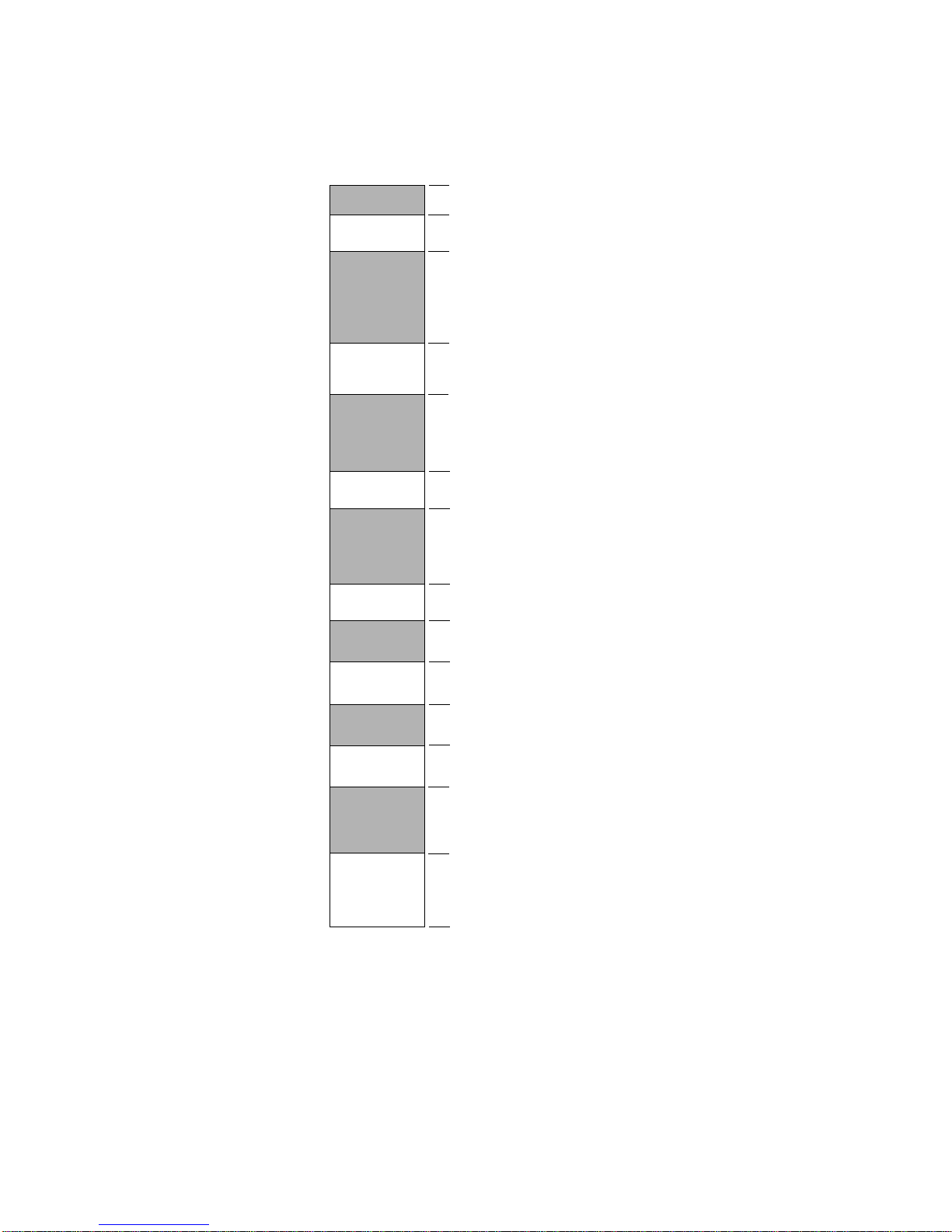
Because the CPU360 module uses the programmable chip select outputs for the rom,
ramand i/o areas, the address map is determined by the software at startup. A suggested
address map is shown in the following table.
Figure 1. Address map
0x0
0x07FFFFFF
0x08000000
Eprom (max 2M)
G64 bus
0xFFFFFFFF
Dram (1M)
Unused
0x085FFFFF
0x08600000
0x001FFFFF
0x00200000
0x01FFFFFF
0x02000000
0x030FFFFF
0x03100000
0x02FFFFFF
0x03000000 Sram (128k)
Eeprom (128k)
Unused
Unused
0x020FFFFF
0x02100000
0x0307FFFF
0x03080000
0x0317FFFF
0x03180000
0xFFFEFFFF
0xFFFF0000
0xFFFF084F
0xFFFF0850
I/O
0x06FFFFFF
0x07000000 SIM360 internal registers
0x07000FFF
0x07001000
Unused

Issue 4 CPU360 Hardware Manual
Copyright © 2004 Quin Systems Limited Page 7
2.4 G64 Bus Address Map
The address map within the G64 bus address space is shown below. Note that the G64
data bus is 16 bits wide, but is accessed on the 32 bit processor bus to allow for the
optional 68040 cpu. Thismeans that G64bus locations are accessed onalternate words.
Figure 2. G64 bus address map
0x08000000
0x082FFFFF
0x08300000
0x08FFFFFF
0x085FFFFF
0x08600000
Unused
G64 bus : VMA
0x084FFFFF
0x08500000
0x080FFFFF
0x08100000
0x083FFFFF
0x08400000
0x081FFFFF
0x08200000
Synchronous 2 MHz
G64 bus : VPA
Synchronous 2 MHz
G64 bus : VMA
Synchronous 1 MHz
G64 bus : VPA
Synchronous 1 MHz
G64 bus : VMA
Asynchronous
G64 bus : VPA
Asynchronous

Issue 4 CPU360 Hardware Manual
Copyright © 2004 Quin Systems Limited Page 8
2.5 I/O Address Map
The address map for the CPU360 I/O devices is shown below. Note that these devices
are all 8 bits wide, but are accessed on the 32 bit processor bus toallow for the optional
68040 cpu. This means that the device registers are accessed on every 4th byte only.
Figure 3. I/O address map
0xFFFF0000
0xFFFF083F
0xFFFF0840
0xFFFFFFFF
Unused
82527 CAN controller 0
0xFFFF03FF
0xFFFF0400
0xFFFF084F
0xFFFF0850
0xFFFF07FF
0xFFFF0800
(256 bytes)
82527 CAN controller 1
(256 bytes)
RTC72423 real time clock
(16 bytes)
Z8536 CIO
(4 bytes)

Issue 4 CPU360 Hardware Manual
Copyright © 2004 Quin Systems Limited Page 9
2.6 68360 Internal Registers
In the 68360 processor, the internal registers in the SIM module and the dual port ram
for the communications processor module (CPM) occupy an 8k byte block. This block
is located on any 8k byte boundary by programming the module base address register
MBAR. The standard software in the PTS systems locates the internal memory at
address 0x07000000.
The MBAR is located at address 0x0003FF00 in cpu space. Note that this does not
conflict with the CS0 chip select address range, as any cpu space access to any global
internal registers does not assert external chip select pins. Accessing the MBAR
requires the use of the MOVES instruction with the SFC or DFC source/destination
function code registers containing the function code for cpu space. Please refer to page
6-3 in the 68360 User’s Manual for more details.
2.7 Memory Control Signals
The port E pins need to be programmed for use with the memory configuration used on
the CPU360 board by programming the port E pin assignment register PEPAR. Set bit
7 to 1 to enable /WE0-3 instead of A28-31. Set bit 6 to 1 to enable the AMUX function
for dram address multiplexer control. Set bits 4 and 2 to 0 to select the /CAS0-3
functions for the dram column address strobes. For more details on setting up the
memory controller and chip select pins, please refer to the 68360 User’s Manual,
chapter 6.
2.8 Memory Sizes
The CPU360 issue D supports the following memory sizes.
EPROM 256k×32, 512k×32, or 1M×32 (four devices)
DRAM 256k×32 or 1M×32 (factory fitted only)
SRAM 128k×8 or 512k×8 (factory fitted only)
EEPROM 128k×8, 256k×8, or 512k×8.
Note that the larger size dram and sram options must be specified when the CPU360
board is ordered, as they are surface mount packages and are soldered directly to the
board.
Also note that the use of larger memory devices may require software changes to
correctly set up the programmable chip select pins on the 68360 processor.
The CPU360 issue E supports the same memory, except that the EPROM is flash
memory, factory fitted. Default is four devices giving 512k×32.

Issue 4 CPU360 Hardware Manual
Copyright © 2004 Quin Systems Limited Page 10
2.9 Communications Ports
The serial communications ports on the CPU360 are very flexible, and use the CPM
communications processor module on the 68EN360 cpu. The four ports are allocated
as follows to the four serial communications controllers (SCCs) on the 68EN360.
SCC1 Ethernet
SCC2 Daughter board (for example, isolated RS-485 for Bitbus)
SCC3 Serial port B
SCC4 Serial port A
The 68EN360 cpu has some software control over various functions of each port,
usually by means of programmable output port pins.
2.10 Ethernet Port
The Ethernet port uses all of the signal lines available to SCC1.
PA0 RXD1
PA1 TXD1
PC0 TENA
PC4 CLSN
PC5 RENA
PA8 TCLK1
PA9 RCLK1
The Ethernet transceiver device, the 68160, has several programmable functions. These
are controlled by output lines on port B. Refer to the 68160 data sheet for more details.
PB10 Twisted pair enable
PB11 Twisted pair auto polarity check
PB12 /Twisted pair full duplex
PB13 /Twisted pair heartbeat
PB14 Auto twisted pair detect
PB15 Loopback
PB16 Standby

Issue 4 CPU360 Hardware Manual
Copyright © 2004 Quin Systems Limited Page 11
2.11 Daughter Board Port
Serial channel SCC2 is connected to daughter board socket XS6. It uses the following
port pins.
PA2 RXD2
PA3 TXD2
PC1 RTS2
PC6 CTS2
PC7 CD2
PA10 TCLK2
PA11 RCLK2
PB4 MODE0
PB5 MODE1
The function of these pins depends on the particular hadrware present on the daughter
board. Standard daughter boards will be made available for specific communications
interfaces as required. For example, a Bitbus interface board provides an isolated
RS-485 interface with software control using the mode signals to select between
synchronous or self-clocked modes, and the data rate for self-clocked operation. The
daughter board uses XS3 and/or XS5 to bring its external signals out to two D type
sockets on the CPU360.

Issue 4 CPU360 Hardware Manual
Copyright © 2004 Quin Systems Limited Page 12
2.12 Serial Ports
The two standard serial ports use programmable RS-232/485 transceivers. These are
controlled by output port signalsfrom the processor, and need to beset up appropriately
by the system software.
Port B uses the following pins.
PA4 RXD3
PA5 TXD3
PC2 RTS3
PC8 CTS3
PC9 CD3
Port A uses the following pins.
PA6 RXD4
PA7 TXD4
PC3 RTS4
PC10 CTS4
PC11 CD4
Each port may be set up for RS-232, RS-485 point-to-point (enabled), or RS-485
multidrop with tristate control. When RS-232 mode is selected, ports A and B support
hardware handshake using the RTS/CTS signals, and an optional CD carrier detect
signal for use with modems.
Port B (SCC3)
Mode PB8 PC2
RS-2320 RTS3
RS-4851 tristate control (0=enabled, 1=disabled)
Port A (SCC4)
Mode PB9 PC3
RS-2320 RTS4
RS-4851 tristate control (0=enabled, 1=disabled)
Port Aalsohas a jumpertoallow it tobe forced intoRS-232modeifrequired. Normally
a link is fitted to J9 pins 1–2 for software control as described above. If this link is
removed, then port A is set to RS-485 mode. If the link is fitted to J9 pins 2–3, then
RS-232 mode is selected.

Issue 4 CPU360 Hardware Manual
Copyright © 2004 Quin Systems Limited Page 13
2.13 Serial Eeprom
The following port pins are used for the serial eeprom device. This is normally an SPI
compatible device, a Xicor X25040, having a capacity of 4k bits (512×8).
PB0 /SPISEL serial eeprom enable
PB1 SPICLK serial eeprom clock
PB2 SPIMOSI data output to serial eeprom
PB3 SPIMISO data input from serial eeprom
2.14 Other Signals
Other port lines are used as follows.
PA12 Green LED (low = on)
PA13 Red LED (low = on)
PA14 Hardware watchdog trigger
PA15 Hardware watchdog status (low = watchdog tripped)
These red and green LEDs indicate start-up self-test in the PTS firmware: on together
during test, then green only as the system runs.
2.15 CANbus Ports
The CPU360 module supports two separate CANbus ports. These use the Intel 82527
CANbus controller, which supports both CAN 1 and CAN 2 protocols. The hardware
implementation of the physical layer is fully isolated and uses the Philips 82C250
transceiver which operates at a bit rate ofupto 1Mbit/second. It complies with theCAN
in Automation (CiA) draft standard DS102Version2.0, CAN Physical Layer for
Industrial Applications.
The CANbusimplementationrequires anexternal powersupply to provide power to the
isolated transceivers. Ifthe CANbus is disconnected, or the powersupply is not present,
then the CANbus interface will not operate. An optocoupler device is connected to the
CANbus network power supply, and allows software to detect whether or not it is
present.
2.16 Daughter Board
The CPU360 board supports a range of standard communications modules made by
Hilscher GmbH. These offer several different protocols and interfaces, including
Profibus and Interbus-S. The modules connectto the CPU360 board via daughter board
connector XP1. XS2 and XS4 connect status and error signals to the front panel LED
indicators. The communications link signals use XS5 to connect to one of the 9 way D
sockets on the CPU360. The high speed communications modules use a local processor
with a dual port memory interface to the CPU360. These use a local serial port to
configure the communications module, which is via XS3 to the second 9 way D socket.

Issue 4 CPU360 Hardware Manual
Copyright © 2004 Quin Systems Limited Page 14
3. Configuration
3.1 Eprom/Flash Pin 31 : J1
J1 selects the signal connected to pin 31 of the eprom or flash rom devices in sockets
IC3-6. For 27C020 or similar eproms (256k ×8), link pins 1 and 2 only. For 27C040
eproms (512k×8) or larger, link pins 1–2 and 3–4. For all flash roms, no links should
be fitted to J1.
3.2 Eprom/Flash Pin 1 : J2
J2 selects the signal connected to pin 1 of the eprom or flash rom devicesin sockets IC3-
6.For most eproms and flash devices, no link should be fitted to J2. For 27C080 eproms
(1M×8), link pins 1 and 2. For 29F040 flash roms, link pins 2 and 3.
3.3 Dram Burst Addressing : J3
Jumper J3 allows the dram memory to be configured for burst cycles when used with
the optional 68040 processor. For normal operation with the 68360 processor, link pins
1–3 and 2–4. To allow burst cycle operation with the optional 68040 processor, link
pins 3–5 and 4–6.
3.4 Serial Eeprom Write Protect : J4
To write protect the serial eeprom device IC16, fit a link to jumper J4.
3.5 Interrupt Configuration : J5
Jumper J5 is used to connect various interrupt sources to the seven processor interrupt
inputs.
Figure 4. Interrupt configuration : J5
The normal configuration is with the G64 bus /FIRQ interrupt connected to level 6, and
the G64 bus /IRQ signal connected to irq level 2. The standard firmware supplied with
the PTS system uses these interrupt levels.
/IRQ7 : 1
/IRQ6 : 3
/IRQ5 : 5
J5
2 : /G64NMI
4 : /G64FIRQ
6 : /COMIRQ (from daughter board)
/IRQ4 : 7
/IRQ3 : 9
/IRQ2 : 11
8 : /COMIRQ
10 : /COMIRQ
12 : /G64IRQ
/IRQ1 : 13 14 : /CIOIRQ

Issue 4 CPU360 Hardware Manual
Copyright © 2004 Quin Systems Limited Page 15
3.6 Reset and Watchdog : J6
Jumper J6 sets up options for the hardware watchdog and reset device. Link pins 1 and
2 to give a manual reset signal to the processor. Link pins 3 and 4 to enable the external
hardware watchdog. Link pins 5 and 6 to enable the external hardware reset to the
processor. Pins 7 and 8 connect the rechargeable battery to the VBB supply rail for the
battery backed memory and real time calendar/clock devices. The normal configuration
is with links fitted to pins 5–6 and 7–8.
Figure 5. Reset and watchdog : J6
3.7 Processor Configuration : J7
Jumper J7is used to set the processor configuration. For normal usewith the 68360 cpu,
link J7 pins 1–2, 3–4 and 7–8. For use with the optional 68040 cpu, link J7 pins 5–6
only.To disable the MMUona full 68040 cpu, link J7pins 11 and 12.This hasnoeffect
on the 68360 cpu, or on other variants of the 68040 such as the 68EC040 or 68LC040.
For JTAG testing, link J7 9-10 unless the 68040 is fitted.
Figure 6. Processor configuration : J7
2 : 0V
4 : CPU PA14
6 : /Hardware Reset
J6
/Manual Reset : 1
Watchdog trigger : 3
/Reset to CPU : 5 8 : Battery V+VBB battery supply : 7
2 : /Reset
4 : /Reset
6 : /Reset
J7
CONFIG0 : 1
CONFIG1 : 3
CONFIG2 : 5 8 : /DSACK1/DSACK0 : 7
68040 TDO : 9 10 : 68360 TDO
/MDIS : 11 12 : 0V

Issue 4 CPU360 Hardware Manual
Copyright © 2004 Quin Systems Limited Page 16
3.8 CIO Clock Frequency : J8
Jumper J8 sets the Z8536 CIO peripheral clock frequency as a power of 2 division of
the main processor clock. The normal configuration is for a CIO clock of 6MHz from
a main processor clock o f 24MHz.
Figure 7. CIO clock frequency : J8
A link fitted connects the clock select line to 0V. The table below shows the clock
division ratios for all link settings, and the peripheral clock speeds fo r a 24MHz main
processor clock.
A B C Divisor 24 MHz
in in in 2 12 MHz
out in in 4 6 MHz (default)
in out in 8 3 MHz
out out in 16 1.5 MHz
in in out 32 750 kHz
out in out 64 375 kHz
in out out 128 187.5 kHz
out out out 256 93.75 kHz
The clock oscillator enable input (pinS) is also brought to J8. This is to allow the clock
to be disabled during board testing, and is not used in normal operation..
2 : 0V
4 : 0V
6 : 0V
J8
A : 1
B : 3
C : 5 8 : 0VS : 7

Issue 4 CPU360 Hardware Manual
Copyright © 2004 Quin Systems Limited Page 17
3.9 Serial Port A Override : J9
The serial ports on the CPU360 module are configured by the software for RS-232 or
RS-485 as required, to reduce the number of jumpers that need to be configured by the
customer for different applications. Jumper J9 allows the software configuration for
port A to be overridden for testing. For normal operation under software control, link
J9 pins 1 and 2. To force RS-232 operation, link pins 2 and 3. To force RS-485
operation, remove the link.
Figure 8. Serial port A override : J9
3.10 Static Ram Size : J10
The CPU360 module can support a 128k×8 or a 512k×8 static ram device. Jumper J10
sets the appropriate address line configuration. For normal operation with a 128k ×8
device (e.g. HM628128), link J10 pins 1 and 2. For use with a 512k×8 device (e.g.
HM628512), link pins 2 and 3. Note that the larger static ram is only available if
specified when the CPU360 is ordered, as the device is in a surface mount package and
is soldered directly to the circuit board.
Figure 9. Static ram size : J10
3.11 CANbus Interrupts : J11
Jumper J11 is used to set up the interrupt signals from the two CANbus interfaces. Note
that the two interfaces may use the same interrupt or two different processor interrupts
if required. The defaults shown cater for SERVOnet and ‘synchro2’ communications.
Figure 10. CANbus interrupts : J11
J9
CPU PB9 : 1
Port A select : 2
0V : 3
J10
Pull-up to +5V :
IC13 pin 30 : 2
A19 : 3
2 : /IRQ5
4 : /IRQ4
6 : /IRQ3
J11
/CAN0 IRQ : 1
/CAN0 IRQ : 3
/CAN0 IRQ : 5 8 : /IRQ5/CAN1 IRQ : 7
/CAN1 IRQ : 9 10 : /IRQ4
/CAN1 IRQ : 11 12 : /IRQ3
Table of contents