Radxa ROCK 3 User manual

Introduction
This guide is written for using Radxa CM3 SoM with the CM3 IO board. The purpose is to learn the
details of the boards as well as how to prepare and set up for basic use.
Overview
What you need
•Necessary
•CM3(any variant) + CM3 IO board
•If the CM3 doesn't have eMMC, a micro SD card larger than 8GB is required for OS
•Power supply
oThe main PSU input (DC) is a 2.1mm DC tip positive +12V(only) input.
•Monitor and HDMI Cable
oCM3 IO board is equipped with a full sized HDMI connector. HDMI capable monitor is
recommended.
oHDMI EDID display data is used to determine the best display resolution. On monitors
and TVs that support 1080p (or 4K) this resolution will be selected. If 1080p is not
supported the next available resolution reported by EDID will be used. This selected
mode will work with MOST but not all monitors/TVs.
•USB to TTL serial cable

oCM3 IO board exports a dedicated serial console for CPU, which can access the low
level debug message.
•Micro USB cable
oIf you want write image to CM3 eMMC from USB OTG port or use fastboot/adb
commands you need a micro USB cable to connect CM3 IO board and PC.
Power on
Plug in the 12V DC, the CM3 should automatically boot. If the CM3 doesn't have eMMC or the eMMC
is empty, plug in the micro USB to host PC, host PC should detect the CM3 in maskrom mode.
Install image to CM3
•Install image to SD card, refer microSD card installation
•Install image to eMMC, refer Install to eMMC from USB port (Radxa CM3 IO)
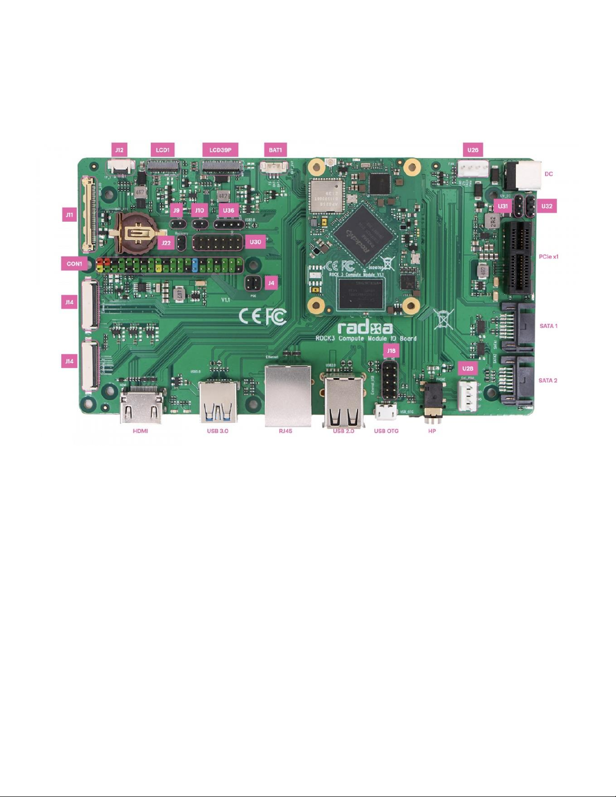
USB 3.0
There is one USB 3.0 A port on the IO board, supporting 5.0Gbps. The USB 3.0 function is shared
with SATA2, a 1in->2out mux CH482D is used for function switching to USB 3.0 or SATA2. GPIO3_C7
is used for the route select, When GPIO3_C7 is low, signal route to USB3.0, when GPIO3_C7 is high,
signal route to SATA2.
Current output limit for the USB 3.0 is 2A.
PCIe Slot
There is one PCIe x1 slot on the IO board, supporting 5.0Gbps. The PCIe function is shared with
SATA1, a 1in->2out mux CH482D is used for function switching to PCIe or SATA1. GPIO3_C6 is used
for the route select, When GPIO3_C6 is low, signal route to PCIe, when GPIO3_C7 is high, signal
route to SATA1.
The PCIe on the CM3 meets PCIe 2.1 specification and support one lane and Root Complex mode
only. PCIe slot power is directly from +12V DC, make sure the power supply can provide enough
current for the PCIe card.
SATA1&2
IO board has two SATA ports compatible with Serial ATA 3.3 and AHCI Revision 1.3.1, SATA 1 is
shared with USB 3.0 and SATA 2 is shared with PCIe, set the corresponding signal route to use it.
Connector U28 can be used for SATA power, the +12V of U28 is directly from the +12V DC, make
sure the power supply can provide enough current for the HDD.
Micro USB
The Micro USB port on the IO board supports host and device mode, it's used for firmware installing
to eMMC from host PC or using ADB debugging. Note: When in maskrom mode, the USB OTG is
forced in device mode.
Other Pinout
LCD1 & LCD2
•LCD1: MIPI DSI0 or LVDS

•LCD2: MIPI DSI1
Pin
Name
1
VCC_LEDA2
2
VCC_LEDA2
3
VCC_LEDA2
4
NC
5
VCC_LEDK2
6
VCC_LEDK2
7
VCC_LEDK2
8
VCC_LEDK2
9
GND
10
GND
11
MIPI_DSI_TX_D2P
12
MIPI_DSI_TX_D2N
13
GND
14
MIPI_DSI_TX_D1P
15
MIPI_DSI_TX_D1N
16
GND
17
MIPI_DSI_TX_CLKP
18
MIPI_DSI_TX_CLKN
19
GND
20
MIPI_DSI_TX_D0P
21
MIPI_DSI_TX_D0N
22
GND
23
MIPI_DSI_TX_D3P

24
MIPI_DSI_TX_D3N
25
GND
26
NC
27
RESET
28
GND
29
VCC_1V8
30
VCC_LCD_MIPI
31
VCC_LCD_MIPI
J11
•eDP 40P
Pin
Name
1
NC
2
GND
3
EDP_TX_D3N
4
EDP_TX_D3P
5
GND
6
EDP_TX_D2N
7
EDP_TX_D2P
8
GND
9
EDP_TX_D1N
10
EDP_TX_D1P
11
GND
12
EDP_TX_D0N
13
EDP_TX_D0P
14
GND

15
EDPTX_AUXP
16
EDPTX_AUXN
17
GND
18
VCC3V3_LCD
19
VCC3V3_LCD
20
VCC3V3_LCD
21
VCC3V3_LCD
22
NC
23
GND
24
GND
25
GND
26
GND
27
NC
28
GND
29
GND
30
GND
31
GND
32
LCD0_BL_EN
33
LCD0_BL_PWM5
34
NC
35
NC
36
VCC12V_LCD
37
VCC12V_LCD
38
VCC12V_LCD
39
VCC12V_LCD

40
NC
41
NC
42
NC
J12 & J13
•Touch Panel
Pin
Name
1
GND
2
SCL_3V3
3
SDA_3V3
4
INT_3V3
5
RST_3V3
6
VCC_TP
J14 & J15
•2x MIPI CSI
Pin
Name
1
RESET
2
PWDN
3
CAM_CLKOUT
4
GND
5
I2C_SCL
6
I2C_SDA
7
NC
8
1V2
9
NC
10
2V8

11
1V8
12
GND
13
MIPI_CSI_RX_D0P
14
MIPI_CSI_RX_D0N
15
NC
16
MIPI_CSI_RX_D1P
17
MIPI_CSI_RX_D1N
18
GND
19
MIPI_CSI_RX_CLK0P
20
MIPI_CSI_RX_CLK0N
21
GND
22
NC
23
NC
24
GND
25
NC
26
NC
U26
Pin
Name
1
GND
2
12V
3
3.3V
4
PWM
U31
Name
Number
WL_nDis
1

GND
2
BT_nDis
3
U32
Name
Number
PWRON_KEY
1
GND
2
RUN_PG(NC)
3
J9
J10
U36
Name
Number
5V0_USB30
1
USB2_HOST3_DM
2
USB2_HOST3_DP
3
GND
4
U30
Name
Number
GND
1
NRPIBOOT(NC)
2
GND
3
EEPROM_NWP
4
AIN0(NC)
5
AIN1(NC)
6
GND
7
SYNC_IN(NC)
8
SYNC_OUT(NC)
9

GND
10
TV_OUT(NC)
11
GND
12
RUN_PG(NC)
13
PWRON_KEY
14
J18
Name
Number
VCC5V0_USB2
1
VCC5V0_USB2
2
USB3_DM
3
USB4_DM
4
USB3_DP
5
USB4_DP
6
GND
7
GND
8
NC
9
NC
10
U28
CON1
General purpose input-output (GPIO)
connector
Radxa CM3 IO has a 40-pin expansion header. Each pin is distinguished by color.
1. Hardware V1.1

GPI
O
num
ber
Functio
n4
Function3
Function2
Funct
ion1
Pi
n#
Pi
n#
Function
1
Function2
Function3
Func
tion4
GPI
O
num
ber
+3.3V
1
2
+5.0V
14
PWM2_
M1
SPI0_MOSI_
M0
I2C2_SDA_
M0
GPIO
0_B6
3
4
+5.0V
13
PWM1_
M1
SPI0_CLK_
M0
I2C2_SCL_
M0
GPIO
0_B5
5
6
GND
125
SDMMC2_P
WREN_M0
I2S1_SDI3_
M1
GPIO
3_D5
7
8
GPIO0_
D1
UART2_TX
_M0
25
GND
9
10
GPIO0_
D0
UART2_R
X_M0
24
23
UART0_CTS
n
PWM0_M1
GPIO
0_C7
11
12
GPIO3_
C7
I2S1_SCLK
_TX_M1
SDMMC2_
D1_M0
119
15
PWM0_M0
GPIO
0_B7
13
14
GND
19
PWM4
GPIO
0_C3
15
16
GPIO3_
D4
I2S1_SDI2_
M1
SDMMC2_
DET_M0
124
+3.3V
17
18
GPIO3_
D3
I2S1_SDI1_
M1
SDMMC2_
CLK_M0
123
138
I2C4_S
DA_M0
I2S2_SDI_M
1
SPI3_MOSI
_M0
GPIO
4_B2
19
20
GND
136
I2S1_SDO1_
M1
SPI3_MISO
_M0
GPIO
4_B0
21
22
GPIO3_
C6
I2S1_MCL
K_M1
SDMMC2_
D0_M0
118

139
I2C4_S
CL_M0
I2S2_SDO_M
1
SPI3_CLK_
M0
GPIO
4_B3
23
24
GPIO4_
A6
SPI3_CS0_
M0
I2S1_SCLK
_RX
134
GND
25
26
SARAD
C_VIN3
140
I2C2_SDA_
M1
GPIO
4_B4
27
28
GPIO4_
B5
I2C2_SCL_
M1
I2S1_SDO3
_M1
141
137
ISP_PRELIG
HT_TRIG
I2S1_SDO2
_M1
GPIO
4_B1
29
30
GND
21
PWM6
SPI0_MISO
_M0
GPIO
0_C5
31
32
GPIO4_
C0
PWM11_IR
_M1
144
22
PWM7_IR
SPI0_CS0_
M0
GPIO
0_C6
33
34
GND
120
SDMMC2_D
2_M0
I2S1_LRC
K_TX_M1
GPIO
3_D0
35
36
GPIO4_
A7
I2S1_LRCK
_RX_M1
SPI3_CS1_
M0
135
18
PWM3_IR
GPIO
0_C2
37
38
GPIO3_
D2
I2S1_SDI0_
M1
122
GND
39
40
GPIO3_
D1
I2S1_SDO0
_M1
SDMMC2_
D3_M0
121
Other Radxa Motherboard manuals