Realan LR-J1900T User manual

LR-J1900T V1.13 Manual
Motherboard Specification:
Motherboard Size
- ITX170mmX170mm
Processor -Intel® J1900 CPU
RAM
- 1*204PinDDR3L SO-DIMMSlot
-support 1.35V/ DDR3L memory, up to 8G
Expansion BUS
-1 x M.2 slot, support WIFI
-1 x MINI_SATA slot, supportSSD
Rear I/O
-1 x DCINPort
-1 x LAN Port/2 x USB 2.0
-1 x LAN Port
-1 x VGAPort
-1 x USB 2.0Port
-1 x USB 3.0 Port
-1 x HDMI Ports
- 1 x LineOut(Green)
-1 x MIC-IN(Red)
Internal I/O
-1 x 4Pin ATX Pins
-1 x F_PANEL
-2 x Fan Pins(CPU_FAN/SYS_FAN)
-2 x F_USB2.0 Pins,supports 4 x USB2.0
-1 x FUSB2.0 Pin,support 1x USB2.0
-1 x F_AUDIO1
-1 x SPKERS1
-1 x SATA1
-1 x JPWR_SATA
-1 x LVDS_CON1
-1 x INV_VOT1
-6 xCOM Pins
-1 x J_LPT1
-1 x VGA_F1
-1 x JHD
-1 x JCMOS(Default 1-2pin)
-1 x AUTO_ON (Default 1-2pin)
-1 x COM1_SET(Default 3-4pin)
-1 x COM2_SET(Default 3-4pin)
-1 x J485
-1 x GPIO
BIOS
-AMIBIOS
Network
-Integrated 10/100/1000Mbps Gigabit Ethernet
Audio -Realtek ALC662
Power Supply
-4PIN ATX or 12VDC
Environment
-Operating Temp.
:
-10
℃~50℃
-Operating Humidity:0%~95%
Operating system
Windows 7 /Windows 8 /Windows 8.1 /Windows10/Linux

CPU_FAN2CPU_FAN3
LCD_SET
HDD_PWR SATA1
F_USB2
F_USB1
F_USB
SPKERS1 FP_AUDIO
JPS1 JHD
VGA_F1
FPI GPIO COM6
J_LPT
COM5 COM4 COM3 COM2 COM1
AUTO_ON
COM1_SET COM2_SET1
LVDS_PWR
COM2_SET2
J485_422
LVDS_CON1
INV_VOT
DCINHDMI VGA LAN/USB
LAN
USB
MIC LINE
MB Layout
LR_J1900T V1.13

Installation Instructions
Tips:
•
Please don’t remove or damage the QC labelon the board
•Make sure the power off before starting installation or remove motherboard
and others hardwares
•
Hold the board by edges,please don
’
t touch any components or pin of plug
&socket.
•Wear anti-static gloves/wrist strap while touching the integrated circuit
components,such as CPU,RAM etc.
•Put tho
se unused or uninstalled components in static shielding bags or trays.
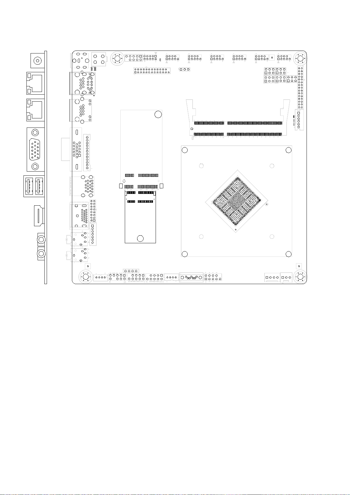
1)Install Memory
The motherboard provides 1 x204-pinDDR3L SO-DIMM slot,Please refer to the
following steps to install your memory bank:
•
Please choose the proper memory bank that matches the motherboard.
•
Please first check the power switch is off before connecting or remove the memory
bank
•
please align the notch of the memory bank with the alignment mark on the socket and
press the memory bank slowly into the socket.
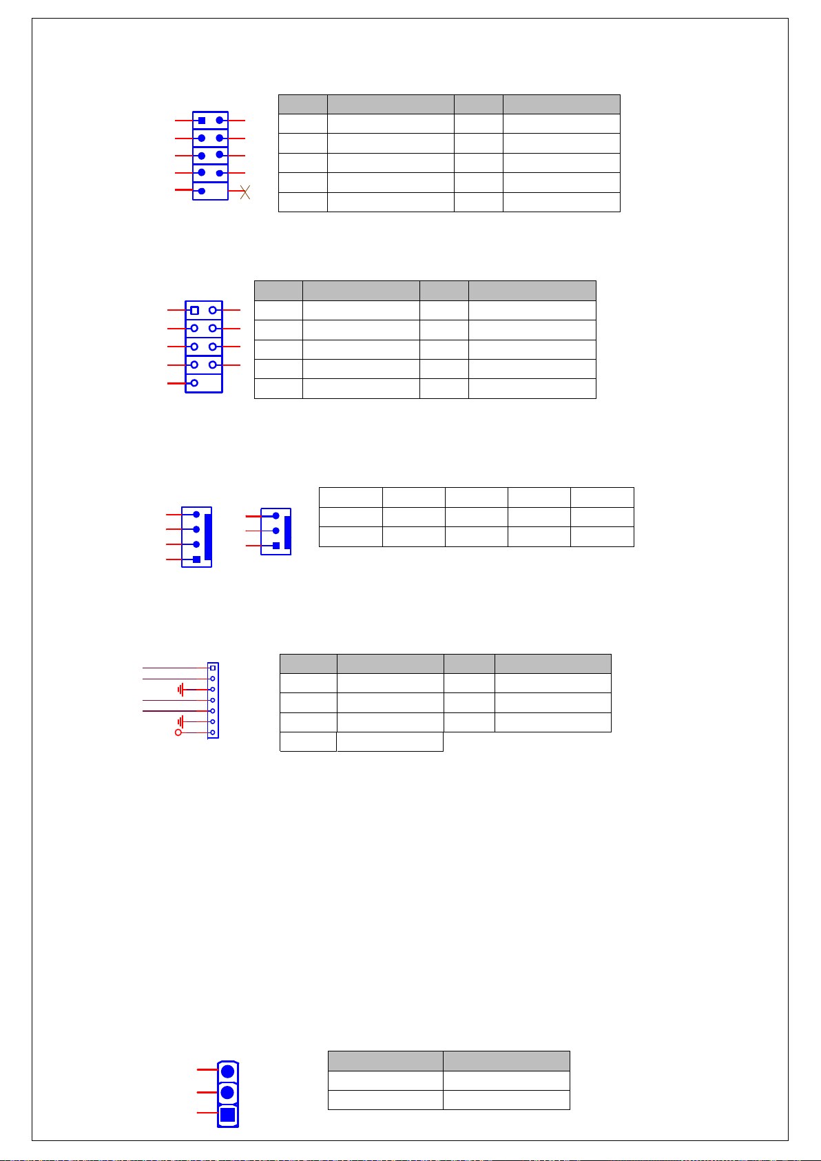
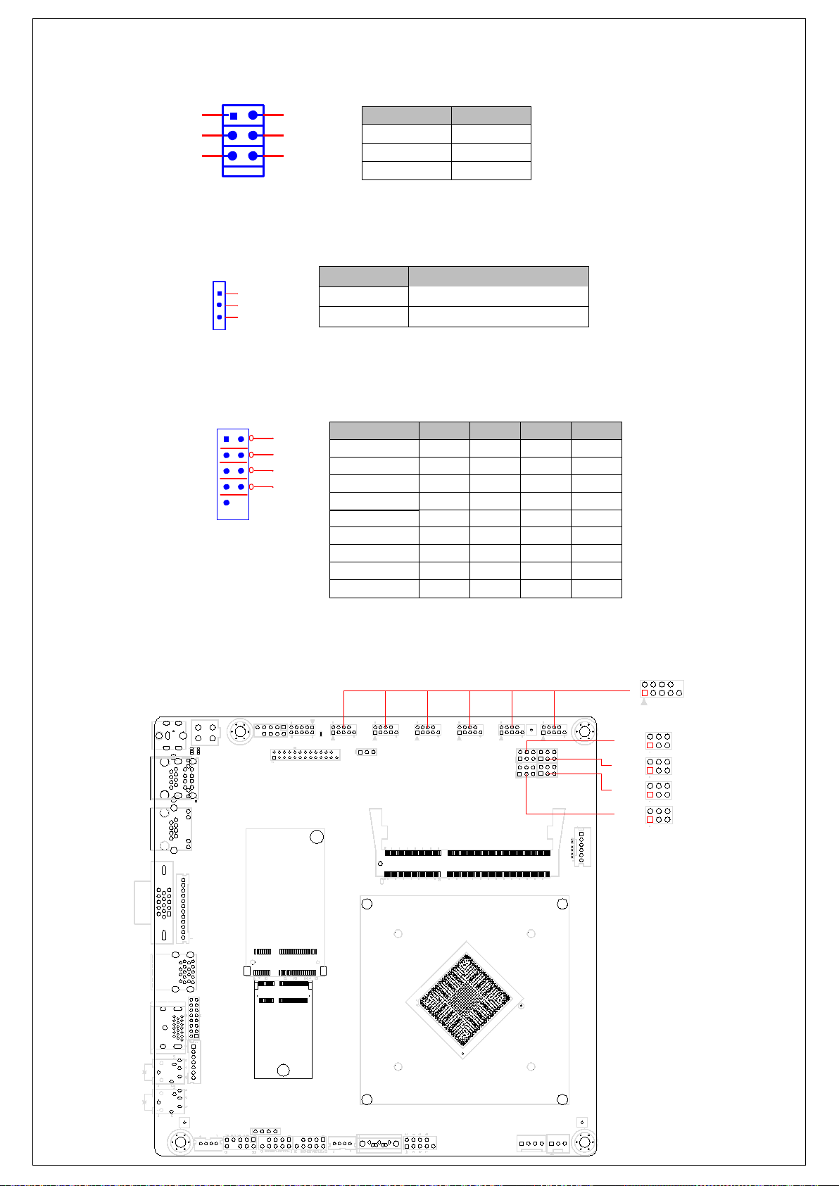
2)Jumper Function Settings
Please refer tofollowing instructions todojumper settings before installing the
motherboard.
2 pinsinterfaces:make jumper cap into pin1 and 2 shorted.
3 pinsinterfaces:make jumper cap into pin1 and 2 shorted.or pin2-3 shorted.
Remark: How to identify the 1st pin of all jumpers and interfaces,Please observe the
word mark on the side of the plug socket, which will be a "1" or bold line or triangular
Symbol -"▲"; And please look at the back of PCB, each with a square shape will be
the PIN 1; and all the jumpers'PIN1 have a white arrow on the side.

GND 2
12V2
GND 1
12V1
2
4
1
3
2.1 ATX12Power
Board provide 1*4Pin ATX power connector, support 12V input/output
ATX_12V
PWR_4P
2.2 Display Port (VGA_F1)
Board
provide
1*12 Pin VGA _F1 connector (Pitch:2.0mm), definition as follow:
2.3
Display Port(
LVDS_CON1)
Board provide 2*15Pin LVDS_CON1 Port(Pitch:2.0mm), definition as follow:
LVDS_CON1
H2X15_2MM
2.4 LVDS (backlight power supply connector)-INV_VOT
Board provide 1*6PIN INVERTPort,(Pitch:2.0mm), definition as follow:
2.5 SATA Power Supply
:
JPWR_SATA1
Board provide 1*4PinSATA Power Connector(Pitch:2.54mm),definition as follow
Pin
1
2
3
4
Signal Name +12V Ground Ground +5V
4
3
2
1
VCC
1
2
VCC
EDID_CLK3
4
EDID_DATA
6
GND
5
GND
8
RXO0--
7
RXO0+
10
RXO1--
9
RXO1+
12
RXO2-11
RXO2+
GND
13
14
GND
16
RXOC-
15
RXOC+
18
RXO3-
17
RXO3+
BDO0-19
20
BDO0+
BDO1-21
22
BDO1+
BDO2-23
24
BDO2+
26
GND
25
GND
28
BCLK-
27
BCLK+
30
BDO3-29
BDO3+
Pin
Signal Name
Pin
Signal Name
1 GND 2 VGA_VSYNC
3 VGA_HSYNC 4 GND
5 VGA_RED(ReD)
6
GND
7 VGA_GRN(Green)
8
GND
9 VGA_BLUE(Blue)10 GND
11 VGA_5VDDA 12 VGA_5VDDCLK
Pin
Signal Name
Pin
Signal Name
1
VCC
2
VCC
3
EDID_CLK
4
EDID_DATA
5
GND
6
GND
7
LVDS_A_DATA0-
8
LVDS_A_DATA0+
9
LVDS_A_DATA1-
10
LVDS_A_DATA1+
11
LVDS_A_DATA2-
12
LVDS_A_DATA2+
13
GND
14
GND
15
LVDS_A_CLK-
16
LVDS_A_CLK+
17
LVDS_A_DATA3-
18
LVDS_A_DATA3+
19
LVDS_B_DATA0-
20
LVDS_B_DATA0+
21
LVDS_B_DATA1-
22
LVDS_B_DATA1+
23
LVDS_B_DATA2-
24
LVDS_B_DATA2+
25
GND
26
GND
27
LVDS_B_CLK-
28
LVDS_B_CLK+
29
LVDS_B_DATA3-
30
LVDS_B_DATA3+
Pin Signal Name Pin Signal Name
1
+12V
2
+12V
3
LVDS_BKL_EN
4
BKLCTRL Backlightbrightness
5
GND
6
GND
VGA_F1
1
2
3
4
5
JP1x12 2.0MM
6
7
8
9
10
11
12
JP1x6
H1x6_2MM
INV_VOT
2
3
4
5
6
1

2.6 J H D definition: HDMI
Board provide 1*2x8pinHDMIport (Pitch2.0mm), definition as follow
JHD
2.7 Parallel port :J_LPT definition
Board provide 2*13Pinprint port (Pitch:2.00mm),definition as follow
J_LPT
2X13_2_2
2.8 Programmable input / output port
(
GPIO
)
Board provide 2*5pinGPIO port(Pitch2.0mm),definition as follow:
GPIO
1 2
3 4
5 6
7 8
9 10
1
2
3
4
5
6
7
8
9
10
11
12
13
14
15
16
17
18
19
20
21
22
23
24
25
1
2
3
4
5
6
7
8
9
10
11
12
13
14
16
15
Pin
Signal Name
Pin
Signal Name
1
HDMI_TXD2_P
2
HDMI_DDC_CLK_R
3
HDMI_TXD2_N
4
HDMI_DDC_DATA_R
5
HDMI_TXD1_P
6
NC
7
HDMI_TXD1_N
8
HPD_CONN
9
HDMI_TXD0_P
10
+5V_HDMI
11
HDMI_TXD0_N
12
GND
13
HDMI_TXC0P
14
GND
15
HDMI_TXC0N
16
GND
Pin
Signal Name
Pin
Signal Name
1
STB
2
AFD
3
PD0
4
LPT_ERR
5 PD1 6 INIT
7 PD2 8 SLIN
9 PD3 10 GND
11
PD4
12
GND
13
PD5
14
GND
15
PD6
16
GND
17
PD7
18
GND
19 LPT_ACK 20 GND
21 LPT_BUSY 22 GND
23 LPT_PE 24 GND
25
LPT_SLCT
26
none
Pin Signal Name Pin Signal Name
1 GPI_0 2 3.3V
3 GPI_1 4 GPO_6
5 GPI_2 6 GPO_7
7 GPI_3 8 GPO_8
9 GND 10 +GPO_9
2.9 Audio port
2.9.1 Speaker:SPKERS1
Board provide 1*4Pin SpeakerPort,definition as follow:
Pin Signal
1
2 AMP_OUT_L+
3 AMP_OUT_R-
4 AMP_OUT_R+
4
3
2
1
2.9.2:FP_AUDIO
Board provide 1* front panel audio port 2*5Pin(Pitch:2.54MM),definition as follow:
Pin Signal Name Pin Signal Name
1 FP_MIC_L 2 GND
3 FP_MIC_R 4 ACZ_DET#_R
5 FP_OUT_R 6 MIC_JD
7 GND
9 FP_OUT_L 10 Lin_JD
FP_AUDIO1
1
3
5
7
9
2
4
6
10
AMP_OUT_L-

2.10 USB Port:F_USB1、F_USB2
Board provide 2*standard USB2.0 Ports 2*5pin(Pitch:2.54mm).definition as follow
F_USB1/F_USB2
1 2
2X5NC9
3 4
5 6
7 7
9
Pin Signal Name Pin Signal Name
1 VCC+5V 2 VCC+5V
3 USB1Date- 4 USB2Date-
5 USB1Date+ 6 USB2Date+
7 GND 8 GND
9 10 OC
2.11 front panel port:F_PANEL
Board provide 1*2x 5PinFront Panel port (Pitch:2.54mm), definition as follow:
F_PANEL
2X5NC10
1 2
3 4
5 6
7 7
9
Pin Signal Name Pin Signal Name
1 HDDLED+ 2 PWRLED+
3 HDDLED- 4 PWRLED-
5 GND 6 POWER-SW
7 RESET-SW 8 GND
9 GND
2.12 fan connector:CPU_FAN2/CPU_FAN3
Board provide CPU_FAN/SYA_FANconnmetctor(Pitch:2.54mm)
Pin 1 2 3 4
CFAN1 Ground +12V Sense PWM
SFAN1 Ground +12V Sense
&38_FAN2&38_FAN3
2.14 Clear CMOSJumper:JCMOS
Board provide1*1x3PINJCMOS connctor,JCMOS:CMOS eraser/save (Pitch:2.54mm)
CMOS is powered by the onboard button cells.Clear CMOS may lead to permanent
elimination of previous system settings and make the system back to the original settings
(factorydefault ).
Steps:
(1) Shut down the computer and disconnect power supply.
(2) Make the jumper cap "JBAT1" Pin2 and 3 shorted for 5~6 seconds,and make it back to
default setting with Pin 1-2 connected ;
(3) Start up computer and press “Delete" to enter BIOS setup.
(4)Press“F9”----“Enter”then reload optimal defaults.
(5) ress “F10 “,Save and Exit.
Pin Signal Name
1-2 Default
2-3 ClearCMOS
JCMOS
2
1
3
pin Signal Name pin Signal Name
1
+5V
2
3
KCLK
4
GND
5
MDAT
6
MCLK
JPS1
KDAT
GND
7
2.13 PS/2 Connector: JPS1
Board provide 1*7Pin PS/2 Connector(Pitch=2.00mm)
MDAT
KDAT
MCLK
KCLK
+V5S
1
HDR1X7
2
3
4
5
6
7

2.16 Auto OnFuntion:AUTO_ON
Board provide1*1x3Pinconnector (Pitch:2.54mm),definition as follow:
AUTO_ON
1
2
3
Pin Signal Name
1-2(Default) Normal
2-3 Auto Power on
2.17 Jumper for LCDResolution:LCD_SEL
Board provide4*1x2Pinconnector (Pitch:2.54mm,definition as follow:
LCD_SEL
4
3
2
1
LCD_SEL 1234
1024X768X6 ON ON ON
1024X768X8 ON ON ON
1280x768x6 ON ON
1280x800x6 ON ON ON
1366x768x6 ON
1366x768x8 ON ON ON
1440x900x8 ON ON
1600x900x8 ON
1920x1080x8 ON
2.15 LVDSPower Jumper
:
LVDS_PWR
Board provide1*2x3pinLCD_SETconnector,(Pitch:2.54mm),definition as follow:
LVDS_PWR
2X3
1 2
3 4
5 6
Pin Signal Name
1-2 +3.3V
3-4 +5
5-6 +12V
COM6 COM5 COM4 COM3 COM2 COM1
COM1_SET COM2_SET1
COM2_SET2J485_422
LR_J1900T V1.13
COM 2 4
3
6
5
8
7 91
COM1_SET 2 4
3
6
5
1
COM2_SET12 4
3
6
5
1
COM2_SET2 2 4
3
6
5
1
J485_422 2 4
3
6
5
1
2.18 Serial ports: COM1、COM2、COM3、COM4、COM5、COM6

Board provide 6* RS232 serial ports, 2*5Pin(Pitch=2.0mm)
COM1
Pin Signal Name Pin Signal Name
1 DCD 2 RXD
3 TXD 4 DTR
5 GND 6 DSR
7 RTS 8 CTS
9 RI 10 NC
NDCD
1 2
NSIN
NSOU T
3 4
NDTR
GND
5 6
NDSR
NRTS
7
NCTS
8
NRI
9
2.18.1 COM Power Jumper:COM1_SET/COM2_SET1
Board provide1*2x3pinCOM_SET connector,adjust power supply by COM1/COM2
(Pitch:2.54mm),definition as follow:
COM_SET
2X3
1 2
3 4
5 6
Pin Signal Name
1-2 +12V
3-4 +DCD
5-6 +5V
2.18.2 RS232/RS422/RS485 Jumper:COM_SET2
Board provide 1*2x3pinCOM_SET2 connector,for adjust signal between RS232/
RS422/RS485 (Pitch:2.54mm),definition as follow:
COM_SET2
2X3
1 2
3 4
5 6
Pin Signal Name
1-2 RS232
3-4 RS422
5-6 RS485
2.18.3 RS422/RS485:J485_422
Board provide1*2x 3pinJ485_422,to connect RS422 or RS485 (Pitch:2.54mm),
definition asfollow:
J485_422
2X3
1 2
3 4
5 6
Pin RS485Signa RS422SignalPin RS485SignalRS422Signal
1 NC 422RX+ 2 NC 422RX-
3 485+ 422TX+ 4 485- 422TX-
5 GND GND 6 GND GND
Table of contents
Other Realan Motherboard manuals
Popular Motherboard manuals by other brands

Linear Technology
Linear Technology DC1780A-A Demo Manual

Linear Technology
Linear Technology DC1485A Demo Manual

Linear Technology
Linear Technology DC1763A Demo Manual

Linear
Linear Analog Devices LTC4040 Demo Manual

Linear Technology
Linear Technology LTC3880 Demo Manual

NS
NS LMX2306TM operating instructions