Realtek RTD2120K User manual

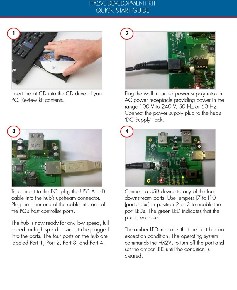
Realtek RTD2120-series
confidential1
RTD2120-series
8051 Embedded Micro-Controller for Monitor
FullyTechnology
Revision
Version 1.06
Last updated: 2007/4/3

Realtek RTD2120-series
confidential2
Revision History
Rev. Description Date
1.02 1. CLKO2( XFR FF01[1] )defaultvalue1 à0
2. PLL_TEST(XFR FF10[7] ) àPLL_STA
3. revise the Reset table”
2006/2/9
1.03 1. revisethe SFR table àdelete address 93, B3
2. addPWM description
3. addpowersupplycurrent
4. add description
AllNC pin must beleft unconnectedorbe connected
to GND.”
2006/8/1
1.04 1. addedRTD2120K,QFP44pinconfig.
2. addedRTD2120K,QFP44pindescription.
2007/1/16
1.05 1. added reset pulse minimum length is 16 MCU clk cycle (page-10) 2007/2/9
1.06 1. modifiedWDT blockdiagram 2007/4/3

Realtek RTD2120-series
confidential3
Overview
This chip isthe micro-processorof LCD monitor. It usestheDesignware DW8051 ofSynopsys
asthe 8051core ofthis chipandis compatible with otherindustry8051series. Also,96Kbyte
FLASHwith 8bitbus is embedded in this chip which is licensedfromTSMC 0.18ume-FLASH
process.Here we use thepackageofPLCC44/LQFP48/QFP44ifwewouldliketohaveadiscrete
MCU controlleror wemake amulti-chippackagewithourLCD monitorcontrollertoformone
chippackage tosave the cost ofpackage andPCB material.
Features
lOperatingvoltage range:3.0Vto3.6V
l8051 core, CPU operating frequencyupto50MHz
l4 clockspermachine cycle
l256-byteinternal RAM
l512-byteexternal dataRAM, including 256-byte DDC RAM(128-byte x 2) and256-byte
generalpurpose RAM
l96K-byte flashmemory, 64k for programand32kfor savingparameter
lTwo DDC portscompliantwithVESADDC1/2B/2Bi/CI
lThree channels ofPWMDAC withprogrammable frequencyfrom 100Kto100Hz
lWatchdogtimerwithprogrammable interval
lThree 16-bitcounters/timers (T0,T1, and T2)
lOne PLLto provide programmable operatingfrequencyandclockoutput, 2 clockoutput
ports
lOne full-duplexserialport
lSix interrupt sourceswith2externalinterrupts
lFour channels of 6-bit ADC
lHardware In System Programming(ISP) capability,nobootcode required
lBuilt-inLow voltageresetcircuit
lEmbedded1.8Vregulator
lCode protection
lAvailable in 44-pinPLCC, 44-pinQFP or 48-pinLQFP package

Realtek RTD2120-series
confidential4
Pin Configurations
P5.5/PWM5
DSCL/P5.6
DSDA/P5.7
RST
ASCL/P3.0/RXD
ASDA/P3.1/TXD
P3.2/INT0
P3.3/INT1
P3.4/T0
P3.5/T1
P6.4
P1.4
P1.5
P1.6
P1.7
NC
NC
NC
VSYNC
P6.7
P6.6/CLKO1
P6.5
P6.3/ADC3
P6.2/ADC2
P6.1/ADC1
P6.0/ADC0
NC
VSS
XI
XO
P7.7
P7.6/CLKO2
P1.3
P1.2
P1.0/T2
VCC
NC
P5.0/PWM0
P5.1/PWM1
P5.2/PWM2
P5.3/PWM3
P5.4/PWM4
P1.1
NC
28
27
26
25
24
23
22
21
20
19
18
40
41
42
43
44
1
2
3
4
5
6
8
7
10
9
12
11
14
13
16
15
17
38
39
36
37
34
35
32
33
30
31
29
RTD2120S
44-PIN
PLCC
23
22
21
20
19
18
17
16
15
14
13
38
39
40
41
43
44
45
46
47
48
2
1
4
3
6
5
8
7
10
9
11
35
36
33
34
31
32
29
30
27
28
26
RTD2120L
48-PIN
LQFP
42
37
12
24
25
P5.5/PWM5
DSCL/P5.6
DSDA/P5.7
RST
ASCL/P3.0/RXD
ASDA/P3.1/TXD
P3.2/INT0
P3.3/INT1
P3.4/T0
P3.5/T1
P6.4
P1.4
P1.5
P1.6
P1.7
NC
NC
NC
VSYNC
P6.7
P6.6/CLKO1
P6.5
P6.3/ADC3
P6.2/ADC2
P6.1/ADC1
P6.0/ADC0
NC
VSS
XI
XO
P7.7
P7.6/CLKO2
P1.3
P1.2
P1.0/T2
VCC
NC
P5.0/PWM0
P5.1/PWM1
P5.2/PWM2
P5.3/PWM3
P5.4/PWM4
P1.1
NC
NC
NCNC
NC

Realtek RTD2120-series
confidential5
P5.5/PWM5
DSCL/P5.6
DSDA/P5.7
RST
ASCL/P3.0/RXD
ASDA/P3.1/TXD
P3.2/INT0
P3.3/INT1
P3.4/T0
P3.5/T1
P6.4
P1.4
P1.5
P1.6
P1.7
NC
NC
NC
VSYNC
P6.7
P6.6/CLKO1
P6.5
P6.3/ADC3
P6.2/ADC2
P6.1/ADC1
P6.0/ADC0
NC
VSS
XI
XO
P7.7
P7.6/CLKO2
P1.3
P1.2
P1.0/T2
VCC
NC
P5.0/PWM0
P5.1/PWM1
P5.2/PWM2
P5.3/PWM3
P5.4/PWM4
P1.1
NC
22
21
20
19
18
17
16
15
14
13
12
2
1
4
3
6
5
8
7
10
9
11
32
33
30
31
28
29
26
27
24
25
23
RTD2120K
44-PIN
QFP
34
35
36
37
38
39
40
41
42
43
44

Realtek RTD2120-series
confidential6
Block Diagram
I2C slave 1
I2C slave 2
6bitADC
6bit ADC
6 bit ADC
6 bitADC
PWM
generator
PWM
generator
PWM
generator
XFR
register
FF00
-FFFF
TSMC FLASH
96Kbyte
MEM_bus
Internal RAM
256 byt`e
IRAM_bus
DW8051_core
DDC_RAM1
128 byte DDC_RAM2
128byte
Routing
Box
FLASH/ISP
interface
Watchdog
timer
Interrupt
Controller
PLL
(clockgen.)
Timer2
Timer0
Timer1
Serial
port0
XTAL
External RAM
Interface
External RAM
256 byte
F900-F97FF980-F9FF
F800-F8FF
00-FF
GPIO

Realtek RTD2120-series
confidential7
Pin Description
Pin No.
PLCC
44 LQFP
48 QFP
44
NameI/OInternal
Pull
Up/Down
Default
output
value
Pin Type
Description
244 40
P5.0/PWM0 I/O-- 1(P5.0)
Open
Drain
Generalpurpose I/O/
PWM0 output
345 41
P5.1/PWM1 I/O-- 1(P5.1)
Open
Drain
Generalpurpose I/O/
PWM1 output
446 42
P5.2/PWM2 I/O-- 1(P5.2)
Open
Drain
Generalpurpose I/O/
PWM2 output
547 43
P5.3/PWM3 I/O-- 1(P5.3)
Open
Drain
Generalpurpose I/O/
PWM3 output
648 44
P5.4/PWM4 I/O-- 1(P5.4)
Open
Drain
Generalpurpose I/O/
PWM4 output
711P5.5/PWM5 I/O-- 1(P5.5)
Open
Drain
Generalpurpose I/O/
PWM5 output
822P5.6/DSCLI/O-- 1(P5.6)
Open
Drain
Generalpurpose I/O/
DVIDDC SCL
933P5.7/DSDA I/O-- 1(P5.7)
Open
Drain Generalpurpose I
/O/
DVI DDC SDA
10 44RST IDown 0Input
High active RESET
11 55ASCL/P3.0/RXD
I/O-- 1(ASCL)
Open
Drain ADC DDC SCL/
Generalpurpose I/O/
RXD
13 87ASDA/P3.1/TXD
I/O-- 1(ASDA)
Open
Drain ADCDDC SDA /
Generalpurpose I/O/
TXD
14 98P3.2/INT0 I/O-- 1(P3.2)
Standard
8051
Generalpurpose I/O/
Externalinterrupt0
15 10 9P3.3/INT1 I/O-- 1(P3.3)
Standard
8051
Generalpurpose I/O/
Externalinterrupt1
16 11 10
P3.4/T0 I/O-- 1(P3.4)
Standard
8051
Generalpurpose I/O/
Timer0
17 12 11
P3.5/T1 I/O-- 1(P3.5)
Standard
8051
Generalpurpose I/O/
Timer1
18 13 12
P7.6/CLKO2 I/OUp1Push-Pull
Generalpurpose I/O/
Clockout 2
19 14 13
P7.7I/OUp1Push-Pull
General purpose I/O
20 15 14
XO
O-- -- -- Crystal out
21 16 15
XI
I-- -- -- Crystalin
22 17 16
VSS
-- -- -- -- Ground

Realtek RTD2120-series
confidential8
Pin No.
PLCC
LQFP
QFP
NameI/OInternal
Pull
Up/Down
Default
output
value
Pin Type
Description
24 20 18
P6.0/ADC0 I/OUp1(P6.0)
Push-Pull
Generalpurpose I/O/
ADC 0 input
25 21 19
P6.1/ADC1 I/OUp1(P6.1)
Push-Pull
Generalpurpose I/O/
ADC 1 input
26 22 20
P6.2/ADC2 I/OUp1(P6.2)
Push-Pull
Generalpurpose I/O/
ADC 2 input
27 23 21
P6.3/ADC3 I/OUp1(P6.3)
Push-Pull
Generalpurpose I/O/
ADC 3 input
28 24 22
P6.4I/OUp1Push-Pull
General purpose I/O
29 25 23
P6.5I/OUp1Push-Pull
General purpose I/O
30 26 24
P6.6/CLKO1 I/OUp1(P6.6)
Push-Pull
Generalpurpose I/O/
Clockout 1
31 27 25
P6.7I/OUp1Push-Pull
General purpose I/O
32 28 26
VSYNC
IDown 0InputVSYNC input
36 33 30
P1.7I/O-- 1Standard
8051/
Push-Pull
General purpose I/O
37 34 31
P1.6I/O-- 1Standard
8051/
Push-Pull
General purpose I/O
38 35 32
P1.5I/O-- 1Standard
8051/
Push-Pull
General purpose I/O
39 36 33
P1.4I/O-- 1Standard
8051/
Push-Pull
General purpose I/O
40 37 34
P1.3I/O-- 1Standard
8051/
Push-Pull
General purpose I/O
41 38 35
P1.2I/O-- 1Standard
8051/
Push-Pull
General purpose I/O
42 39 36
P1.1I/O-- 1Standard
8051/
Push-Pull
General purpose I/O
43 40 37
P1.0/ET2 I/O-- 1(P1.0)
Standard
8051/
Push-Pull
Generalpurpose I/O/
ExternalTimer2
44 41 38
VCC
-- -- -- -- Power
Note: All NC pin mustbeleft unconnectedorbe connectedtoGND.

Realtek RTD2120-series
confidential9
DW8051 micro-processor
The DW8051containedinRTD2120is compatible withindustrystandard 803x/805x and
providesthe followingdesign features andenhancementstothe standard8051 microcontroller:
1. High speedarchitecture
Comparedtostandard8051, theDW8051processor coreprovidesincreased performance by
executinginstructionsina 4-clockbus cycle, asopposedtothe 12-clockbus cycle inthe standard
8051. The shortenedbus timingimproves the instructionexecutionrate formostinstructions bya
factorof three over thestandard8051architectures. Theaveragespeedimprovement fortheentire
instructionsetis approximately 2.5X.
2. StretchMemoryCycles
The stretchmemorycycle feature enables application software toadjust the speedofdata
memoryaccess. The DW8051 can execute the MOVXinstructioninas little as2instruction cycles.
However,it is sometimes desirable tostretchthis value;forexample, toaccess slowmemoryorslow
memory-mappedperipherals suchas UARTs orLCDs.
The three LSBs of the ClockControlRegister(atSFR location8Eh)control the stretchvalue.
You canuse stretchvalues betweenzero andseven. Astretch valueof zero addszeroinstruction
cycles, resultinginMOVX instructions executingin twoinstructioncycles. Astretchvalueof seven
adds seveninstructioncycles, resultinginMOVXinstructions executinginnine instructioncycles.
The stretchvalue canbe changeddynamicallyunder programcontrol.
Bydefault,the stretchvalue resetstoone (three cycle MOVX). For full-speeddatamemory
access, the software mustsetthestretchvaluetozero. The stretchvalue affectsonlydata memory
access. The onlywayto reduce thespeedof program memory(ROM) access is touse a slower clock.
3. Dual DataPointers
The DW8051employsdual data pointers toaccelerate datamemoryblockmoves. The standard
8051 data pointer(DPTR) is a 16-bit value usedto address externaldata RAM orperipherals. The
DW8051 maintainsthe standarddatapointeras DPTR0 atSFR locations 82h and83h.It is not
necessarytomodifycode touse DPTR0.
The DW8051adds a second data pointer(DPTR1) at SFR locations 84h and 85h. The SEL bit in
the DPTR Select register, DPS(SFR 86h), selects the active pointer. WhenSEL= 0,instructions that
use theDPTR willuse DPL0andDPH0. WhenSEL=1, instructions thatuse the DPTR willuse
DPL1 and DPH1. SELis the bit0ofSFR location86h.No other bitsof SFR location86hare used.
All DPTR-relatedinstructions use the currentlyselecteddata pointer. Toswitchthe active
pointer, toggle theSELbit. The fastestwaytodoso is touse theincrement instruction(INC DPS).
Thisrequires onlyoneinstructiontoswitchfrom a source address toa destination address, saving
applicationcode from havingto savesource anddestinationaddresses when doinga blockmove.
Usingdual data pointers providessignificantlyincreasedefficiencywhenmovinglargeblocks of
data.
4. TimerRate Control
One important difference exists betweenthe RTD2120 and80C32regarding timers. Theoriginal
80C32 used a 12clockper cycle scheme fortimers andconsequentlyfor some serialbaud
rates(dependingonthe mode). TheRTD2120architecture normallyruns using4 clocks percycle.
However,inthe area of timers, it will default to a 12 clockpercycle scheme ona reset. Thisallows
existingcodewithreal–time dependencies such as baudrates tooperate properly.If anapplication
needshigher speedtimers orserial baudrates, the timers canbesettorunat the 4clockrate.
Realtek RTD2120-series
confidential10
The ClockControlregister (CKCON –8Eh)determines these timerspeeds. Whenthe relevant
CKCONbit is a logic 1, the device uses 4clocks per cycle togenerate timerspeeds. Whenthe control
bitis settoa zero, the device uses 12clocksfortimerspeeds. The resetconditionisa 0.CKCON.5
selects the speedof Timer 2.CKCON.4selects Timer1andCKCON.3selects Timerzero. Note that
unless a userdesires veryfasttiming, itis unnecessarytoalterthese bits. Notethat the timercontrols
are independent.
Memory Organization
InternalData memory
l256 bytes ofinternal RAM
l128 bytes ofSpecialFunctionRegister(SFR)
External Data memory
l128 bytes ofExternal SpecialFunction Register (XFR)
l256 bytes ofDDCRAM(128-bytex2)
l256 bytes ofgeneralpurpose RAM
l32k bytes offlashforEDID data andotherparameters
External Programmemory
l64k bytes offlashforprogram memory
lThe program content cannot be readout unless user mass erase theflashfirst.
flash0~64K
InternalRAM
Direct/Indirect
addressing
flash 64~96K
Unused
General PurposeRAM
DDC_RAM1&2
Unused
XFR
0000
7FFF
F800
F8FF
F900
F9FF
FF00
FFFF
InternalRAM
Indirect addressing SFR
Direct addressing
Internal DataMemory External DataMemory
0000
FFFF
ExternalProgram Memory
00
7F
80
FF
Reset
There arefivereset sources inRTD2120, asdescribedbelow:
lRST pin
The external resetis high activeandits pulse width must be larger than16mcuclockcycles. The
RST pincanresetthewhole chipof RTD2120.
lLow voltage reset(LVR) andpoweronreset(POR)
The LVRandPOR monitor the powerstatus ofRTD2120. The same as externalreset, the LVR
andPORwillreset the whole chipof RTD2120 whentriggered.
lSoftware reset

Realtek RTD2120-series
confidential11
To activate softwarereset, set FF39[1](SOF_RST). Whensoftware resetis triggered, itwillreset
allmodules exceptdebugmode.
lWatchdogtimer(WDT)
The watchdogtimergenerates reset whenitis overflowed. The watchdogtimerresets almostthe
same modules assoftware resetexceptitself(watchdogtimermodule).
lIn System Programing(ISP)reset
ISPreset will generate whenenteringISPmode. ComparedtoWatchdogtimerreset,ISPmode
resetsalmostthe same modulesas Watchdogtimer exceptitself(ISPmodule).
Debugmode
module Watchdogtimer
module CPUISPmodule and
othermodules
RST pinOOOO
LVR & POR OOOO
Software reset xOOO
WDT resetxxOx
ISPreset xxOx
Note: O= Reset, x=No effect
Interrupt
Six interrupts are provided inRTD2120. Four ofthese are generatedautomaticallybyinternal
operation: timer 0, timer 1, timer2and the serialport interrupt.The othertwointerrupts are triggered
byexternalpins:INT0 and INT1. Moreover, the DDC andIIC interrupts areconnectedtoDW8051
1
INT
source asthe followingfigure.
A_WR_I AWRI_EN
D_WR_I DWRI_EN
128VS_I VSI_EN
STOP_I STOPI_EN
D_OUT_I DOLI_EN
D_IN_I DILI_EN
SUB_I SUBI_EN
SLV_I SLVI_EN
PIN_INT1_EN
pin INT1
toDW8051
1
INT
Timer/Counter
RTD2120 has three timers/counters:T0,T1andT2. T0andT1 are fully compatibleto
timer/counter in standard8051’s. Like timer2 in8052, T2of RTD2120has three operatingmodes:16-
bittimer/counterwithcapture, 16-bitauto-reloadtimer/counter andBaudrate generator. However, T2
of RTD2120 does notsupport Timer2output enable(T2OE)”and downcount enable(DCEN)”. The
SFRs associatedwithTimer2 are listedbelow.
Register Bit7 Bit6Bit5Bit 4 Bit3 Bit2Bit1Bit 0 Addr
T2CONTF2EXF2RCLKTCLKEXEN2TR2 C/T2 CP/RL2
C8h
RCAP2L
CAh

Realtek RTD2120-series
confidential12
RCAP2H
CBh
TL2CCh
TH2CDh
1. 16-bit timer/counter withcapture
The Timer 2capture modeis the same asthe 16-bittimer/counter withthe additionof the capture
registers and controlsignals. If EXEN2 = 0, Timer2is a 16-bit timer/counter . The C/T2bit determines
whetherthe 16-bitcounter countsosc cycles(dividedby4or 12),orhigh-to-low transitions onthe
P1.0 pin.TheTR2bitenables the counter. Whenthe countincrementsfromFFFFh, the TF2flagis set.
The CP/RL2 bit in the T2CON SFR enables thecapture feature. WhenCP/RL2 = 1, a high-to-low
transitiononP1.1 whenEXEN2 = 1causes theTimer2 value tobe loadedinto the capture registers
(RCAP2L and RCAP2H).
2. 16-bit timer/counter withauto-reload
WhenCP/RL2 =0, Timer 2isconfiguredforthe auto-reloadmode. Controlofcounterinput isthe
same as forthe other16-bit countermodes. Whenthecount increments fromFFFFh, Timer 2sets the
TF2 flagandthe startingvalue is reloaded intoTL2 andTH2. The software mustpreloadthe starting
value intotheRCAP2L and RCAP2H registers. WhenTimer 2is inauto-reloadmode, a reloadcanbe
forcedbya high-to-lowtransitionon the P1.1pin, if enabledbyEXEN2=1.
3. Baudrategenerator
SettingeitherRCLKor TCLK to 1configuresTimer2togenerate baudrates forSerial Port0in
serialmode 1or3.Inbaud rate generatormode, Timer2functions inauto-reloadmode. However,
insteadof settingtheTF2 flag,the counter overflow generates a shiftclockfor the serialportfunction.
As innormal auto-reloadmode, the overflowalsocauses thepreloadedstartvalue inthe RCAP2Land
RCAP2H registers tobe reloadedintotheTL2and TH2registers. WheneitherTCLK=1orRCLK =
1, Timer2isforcedintoauto-reloadoperation,regardless of thestate of theCP/RL2 bit. When
operatingas a baud rate generator, Timer2doesnot settheTF2 bit. In this mode, a Timer2interrupt
canonly begenerated bya high-to-low transitionon the P1.1pinsettingthe EXF2 bit, andonlyif
enabledbyEXEN2=1.
The countertime base inbaud rate generatormode is osc/2. Touse anexternalclocksource,
setC/T2 to1andapplythe desiredclocksource tothe P1.0pin.
Special Function Registers(SFR)
Register
Bit7
Bit6
Bit 5
Bit 4
Bit 3
Bit 2
Bit1
Bit0 Reset
Value
(Hex)
Addr
(Hex)
SP 07 81
DPL000 82
DPH000 83
DPL100 84
DPH100 85
DPS0000000SEL00 86
PCONSMOD0
11GF1GF0 STOPIDLE 30 87
TCONTF1 TR1 TF0 TR0 IE1 IT1 IE0 IT0 00 88
TMOD GATE C/TM1 M0 GATE C/T M1 M0 00 89
TL000 8A

Realtek RTD2120-series
confidential13
Register
Bit7
Bit6
Bit 5
Bit 4
Bit 3
Bit 2
Bit1
Bit0 Reset
Value
(Hex)
Addr
(Hex)
TL100 8B
TH000 8C
TH100 8D
CKCONT2M T1M T0M MD2 MD1 MD0 01 8E
SPC_FNC
0000000WRS 00 8F
P1 P1.7P1.6 P1.5P1.4P1.3 P1.2P1.1 P1.0FF 90
MPAGE 00 92
P1_R P1.7 P1.6 P1.5 P1.4 P1.3 P1.2 P1.1 P1.0 FF 93
SCON0SM0 SM1 SM2 REN TB8 RB8 TI RI 00 98
SBUF000 99
P2 P2.7P2.6 P2.5P2.4P2.3 P2.2P2.1 P2.0 00 A0
IE EA 0ET2 ES0 ET1 EX1 ET0 EX0 00 A8
P3 P3.7P3.6 P3.5P3.4P3.3 P3.2P3.1 P3.0FF B0
P3_R P3.7 P3.6 P3.5 P3.4 P3.3 P3.2 P3.1 P3.0 FF B3
IP 10PT2 PS0 PT1 PX1 PT0 PX0 80 B8
T2CONTF2 EXF2 RCLKTCLKEXEN2
TR2 C/T2 CP/RL2
00 C8
RCAP2L00 CA
RCAP2H00 CB
TL200 CC
TH200 CD
PSW CYAC F0RS1RS0 OV F1 P00 D0
ACC 00 E0
B00 F0
External Special Function Registers(XFR)
Pin Share
Register::Pin_share00xFF00
NameBits Read/Write Reset State
Comments
Reserved 7-- 0Reserved
IIC2E6R/W 10: Pin P5.6/DSCL is P5.6, Pin
P5.7/DSDA is P5.7
1: Pin P5.6/DSCL is DSCL,Pin
P5.7/DSDA is DSDA
PWM5E 5R/W 00: Pin P5.5/PWM5 is P5.5
1: Pin P5.5/PWM5 is PWM5
PWM4E 4R/W 00: Pin P5.4/PWM4 is P5.4
1: Pin P5.4/PWM4 is PWM4
PWM3E 3R/W 00: Pin P5.3/PWM3 is P5.3
1: Pin P5.3/PWM3 is PWM3
PWM2E 2R/W 00: Pin P5.2/PWM2 is P5.2
1: Pin P5.2/PWM2 is PWM2

Realtek RTD2120-series
confidential14
PWM1E 1R/W 00: Pin P5.1/PWM1 is P5.1
1: Pin P5.1/PWM1 is PWM1
PWM0E 0R/W 00: Pin P5.0/PWM0 is P5.0
1: Pin P5.0/PWM0 is PWM0
Register::Pin_share10xFF01
NameBits Read/Write Reset State
Comments
A_DDC_PIN_
SEL 7R/W 00: ADC DDC ports areconnectedto
ASDA/ASCL
1: ADC DDC ports areconnectedto
DSDA/DSCL
D_DDC_PIN_
SEL 6R/W 10: DVIDDC ports areconnected to
ASDA/ASCL
1: DVIDDC ports areconnected to
DSDA/DSCL
Reserved 5:3-- 0Reserved
PIN_INT1_E
N 2R/W 1Pin P3.3/INT1”connect to8051INT1
enable
0: disable
1: enable
whenPin P3.3/INT1”is usedas GPIO, this
bit must be0.
CLKO2E1R/W 00: Pin P7.6/CLKO2 is P7.6
1: Pin P7.6/CLKO2 is CLKO2
IIC1E0R/W 10: Pin ASCL/P3.0/Rxd is P3.0/RXD, Pin
ASDA/P3.1/Txd is P3.1/TXD
1: Pin ASCL/P3.0/Rxd is ASCL, Pin
ASDA/P3.1/Txd is ASDA
Register::Pin_share20xFF02
NameBits Read/Write Reset State
Comments
Reserved 7:5-- 0Reserved
CLKO1E4R/W 00: Pin P6.6/CLKO1 is P6.6
1: Pin P6.6/CLKO1 is CLKO1
ADC3E3R/W 00: Pin P6.3/ADC3 is P6.3
1: Pin P6.3/ADC3 is ADC3
ADC2E2R/W 00: Pin P6.2/ADC2 is P6.2
1: Pin P6.2/ADC2 is ADC2
ADC1E1R/W 00: Pin P6.1/ADC1 is P6.1
1: Pin P6.1/ADC1 is ADC1
ADC0E0R/W 00: Pin P6.0/ADC0 is P6.0
1: Pin P6.0/ADC0 is ADC0
I/O port
lEachI/O pinofRTD2120 candrive/sink 4mAandthe internal pull up/down circuit can
drive/sink 10uA.

Realtek RTD2120-series
confidential15
lAll pins have 5V tolerance except fourADC pins: P6.0/ADC0”, P6.1/ADC1”, P6.2/ADC2”
and ”P6.3/ADC3”.
Register::Port5_output_enable 0xFF03
NameBits Read/Write Reset State
Comments
P57OE 7R/W 00: P5.7is input pin
1: P5.7is output pin
P56OE 6R/W 00: P5.6is input pin
1: P5.6is output pin
P55OE 5R/W 00: P5.5is input pin
1: P5.5is output pin
P54OE 4R/W 00: P5.4is input pin
1: P5.4is output pin
P53OE 3R/W 00: P5.3is input pin
1: P5.3is output pin
P52OE 2R/W 00: P5.2is input pin
1: P5.2is output pin
P51OE 1R/W 00: P5.1is input pin
1: P5.1is output pin
P50OE 0R/W 00: P5.0is input pin
1: P5.0is output pin
Register::Port6_output_enable 0xFF04
NameBits Read/Write Reset State
Comments
P67OE 7R/W 00: P6.7is input pin
1: P6.7is output pin
P66OE 6R/W 00: P6.6is input pin
1: P6.6is output pin
P65OE 5R/W 00: P6.5is input pin
1: P6.5is output pin
P64OE 4R/W 00: P6.4is input pin
1: P6.4is output pin
P63OE 3R/W 00: P6.3is input pin
1: P6.3is output pin
P62OE 2R/W 00: P6.2is input pin
1: P6.2is output pin
P61OE 1R/W 00: P6.1is input pin
1: P6.1is output pin
P60OE 0R/W 00: P6.0is input pin
1: P6.0is output pin
Register::Port7_output_enable 0xFF05
NameBits Read/Write Reset State
Comments
P77OE 7R/W 00: P7.7is input pin
1: P7.7is output pin

Realtek RTD2120-series
confidential16
P76OE 6R/W 00: P7.6is input pin
1: P7.6is output pin
Reserved 5:0-- 0Reserved
Register::Port1_pad_type 0xFF09
NameBits Read/Write Reset State
Comments
P17_PPO7R/W 00:P1.7 is standar 8051 I/O
1:P1.7 is Push-Pull output
P16_PPO6R/W 00:P1.6 is standar 8051 I/O
1:P1.6 is Push-Pull output
P15_PPO5R/W 00:P1.5 is standar 8051 I/O
1:P1.5 is Push-Pull output
P14_PPO4R/W 00:P1.4 is standar 8051 I/O
1:P1.4 is Push-Pull output
P13_PPO3R/W 00:P1.3 is standar 8051 I/O
1:P1.3 is Push-Pull output
P12_PPO2R/W 00:P1.2 is standar 8051 I/O
1:P1.2 is Push-Pull output
P11_PPO1R/W 00:P1.1 is standar 8051 I/O
1:P1.1 is Push-Pull output
P10_PPO0R/W 00:P1.0 is standar 8051 I/O
1:P1.0 is Push-Pull output
Register::Port50_pin_reg0xFF50
NameBits Read/Write Reset State
Comments
Reserved 7:1-- 0Reserved
P500R/W 1Input/output value of P5.0
Register::Port51_pin_reg0xFF51
NameBits Read/Write Reset State
Comments
Reserved 7:1-- 0Reserved
P510R/W 1Input/output value of P5.1
Register::Port52_pin_reg0xFF52
NameBits Read/Write Reset State
Comments
Reserved 7:1-- 0Reserved
P520R/W 1Input/output value of P5.2

Realtek RTD2120-series
confidential17
Register::Port53_pin_reg0xFF53
NameBits Read/Write Reset State
Comments
Reserved 7:1-- 0Reserved
P530R/W 1Input/output value of P5.3
Register::Port54_pin_reg0xFF54
NameBits Read/Write Reset State
Comments
Reserved 7:1-- 0Reserved
P540R/W 1Input/output value of P5.4
Register::Port55_pin_reg0xFF55
NameBits Read/Write Reset State
Comments
Reserved 7:1-- 0Reserved
P550R/W 1Input/output value of P5.5
Register::Port56_pin_reg0xFF56
NameBits Read/Write Reset State
Comments
Reserved 7:1-- 0Reserved
P560R/W 1Input/output value of P5.6
Register::Port57_pin_reg0xFF57
NameBits Read/Write Reset State
Comments
Reserved 7:1-- 0Reserved
P570R/W 1Input/output value of P5.7
Register::Port60_pin_reg0xFF58
NameBits Read/Write Reset State
Comments
Reserved 7:1-- 0Reserved
P600R/W 1Input/output value of P6.0

Realtek RTD2120-series
confidential18
Register::Port61_pin_reg0xFF59
NameBits Read/Write Reset State
Comments
Reserved 7:1-- 0Reserved
P610R/W 1Input/output value of P6.1
Register::Port62_pin_reg0xFF5A
NameBits Read/Write Reset State
Comments
Reserved 7:1-- 0Reserved
P620R/W 1Input/output value of P6.2
Register::Port63_pin_reg0xFF5B
NameBits Read/Write Reset State
Comments
Reserved 7:1-- 0Reserved
P630R/W 1Input/output value of P6.3
Register::Port64_pin_reg0xFF5C
NameBits Read/Write Reset State
Comments
Reserved 7:1-- 0Reserved
P640R/W 1Input/output value of P6.4
Register::Port65_pin_reg0xFF5D
NameBits Read/Write Reset State
Comments
Reserved 7:1-- 0Reserved
P650R/W 1Input/output value of P6.5
Register::Port66_pin_reg0xFF5E
NameBits Read/Write Reset State
Comments
Reserved 7:1-- 0Reserved
P660R/W 1Input/output value of P6.6

Realtek RTD2120-series
confidential19
Register::Port67_pin_reg0xFF5F
NameBits Read/Write Reset State
Comments
Reserved 7:1-- 0Reserved
P670R/W 1Input/output value of P6.7
Register::Port76_pin_reg0xFF60
NameBits Read/Write Reset State
Comments
Reserved 7:1-- 0Reserved
P760R/W 1Input/output value of P7.6
Register::Port77_pin_reg0xFF61
NameBits Read/Write Reset State
Comments
Reserved 7:1-- 0Reserved
P770R/W 1Input/output value of P7.7
LowVoltage Reset & Power on Reset
Whenthe voltage level of power supplyis belowVLT, the lowvoltage reset(LVR) generates a chip
reset signal. After the power supplyis above VUT(2.6V), LVR remaininreset statefor65536X’tal
cycle(tPOR)toguarantee the chipexit resetcondition.
VUT
VLT
tPOR
VCC
VSS
INTERNAL RESET
Register::LVR_control 0xFF0A
NameBits Read/Write Reset State
Comments

Realtek RTD2120-series
confidential20
VLT 7:6R/W 0low_threshold_voltage
00:1.8V
01:2.0V
10:2.2V
11:2.4V
reserved5:0-- 00reserved
A/D Converter
RTD2120 has embedded4 channelsof analog-to-digital converter. The ADCs convert analog
inputvoltage onthe four A/D inputpins to four6-bit digital data storedinXFRs(FF0C~FF0F)
sequentially.
The ADC conversionrange isfrom GNDto VDD andthe conversionis linear andmonotonic withno
missingcodes. To start A/D conversion, setSTRT_ADC(FF0B[7])= 1 andthe conversionwillbe
complete inlessthan 12us for 4channels.
Register::ADC_control 0xFF0B
NameBits Read/Write Reset State
Comments
STRT_ADC 7R/W 0Write 1tostart the A/D conversion. Auto
clearwhen A/D Conversionhas been
completed.
0:A/D Conversion has beencompleted
1:A/D Conversion is not completedyet
ADC_TEST 6R/W 00: Normal operation
1: ADC test mode
reserved5:3R/W 0Reserved
BIAS_ADJ 2:1R/W 1ADC bias current adjust
00:15u
01:20u
10:25u
11:30u
CK_SEL0R/W 0Inverse ADC input clockpos/neg
0: pos
1: neg
Register::ADC0_convert_result0xFF0C
NameBits Read/Write Reset State
Comments
ADC0_CONV
_DATA 7:2R3F Converted data ofADC0
reserved1:0-- 00
Register::ADC1_convert_result0xFF0D
This manual suits for next models
4
Table of contents