ScioSense GPX2-EVA-KIT User manual

GPX2-
EVA-KIT
TDC-GPX2 Evaluation Kit
SC-001264-UG User Guide
GPX2-EVA-Kit User Guide
Revision: 5
Release Date: 2021-01-25

PUBLIC INFORMATION
2
GPX2-EVA-Kit User Guide SC-001264-UG-5 / 2021-01-25 / Product
Content Guide
Content Guide ..................................... 2
1Introduction.............................. 3
1.1 Ordering Information .................... 3
2Quick Start Guide ........................ 4
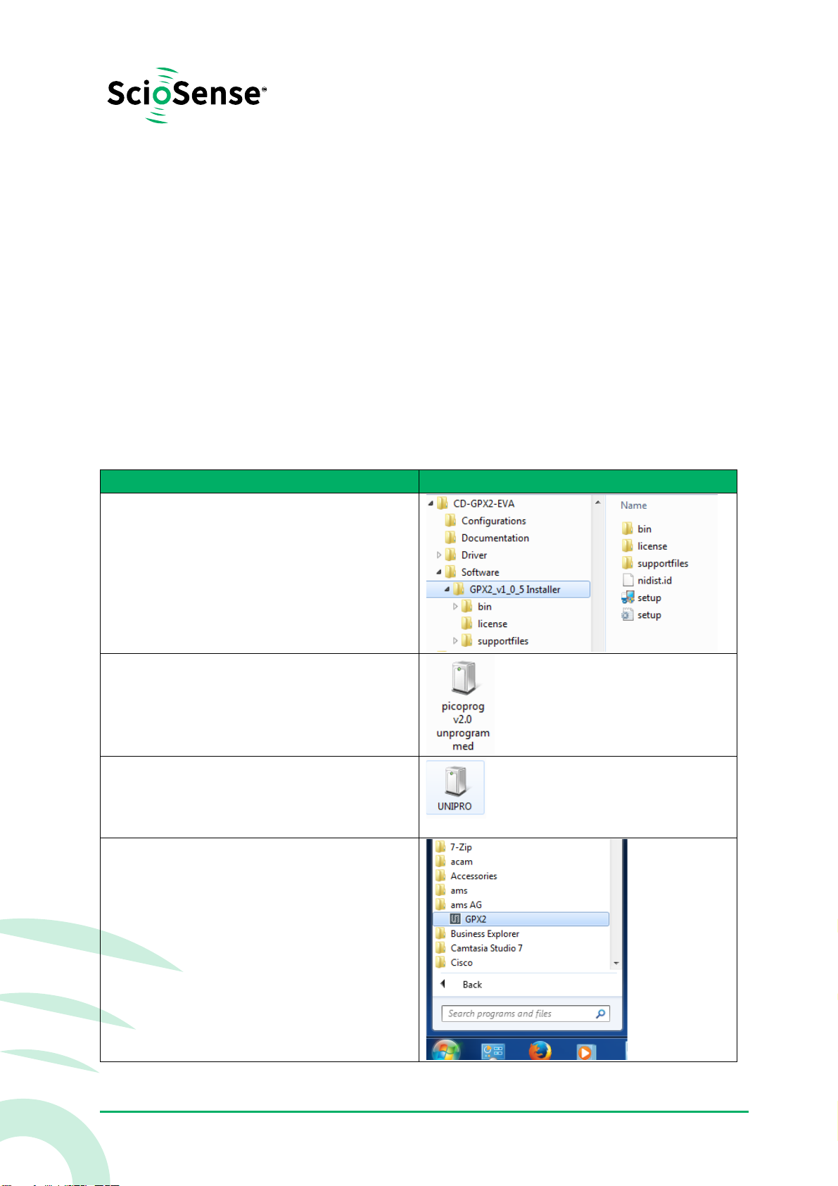
2.1 Install the Software ...................... 4
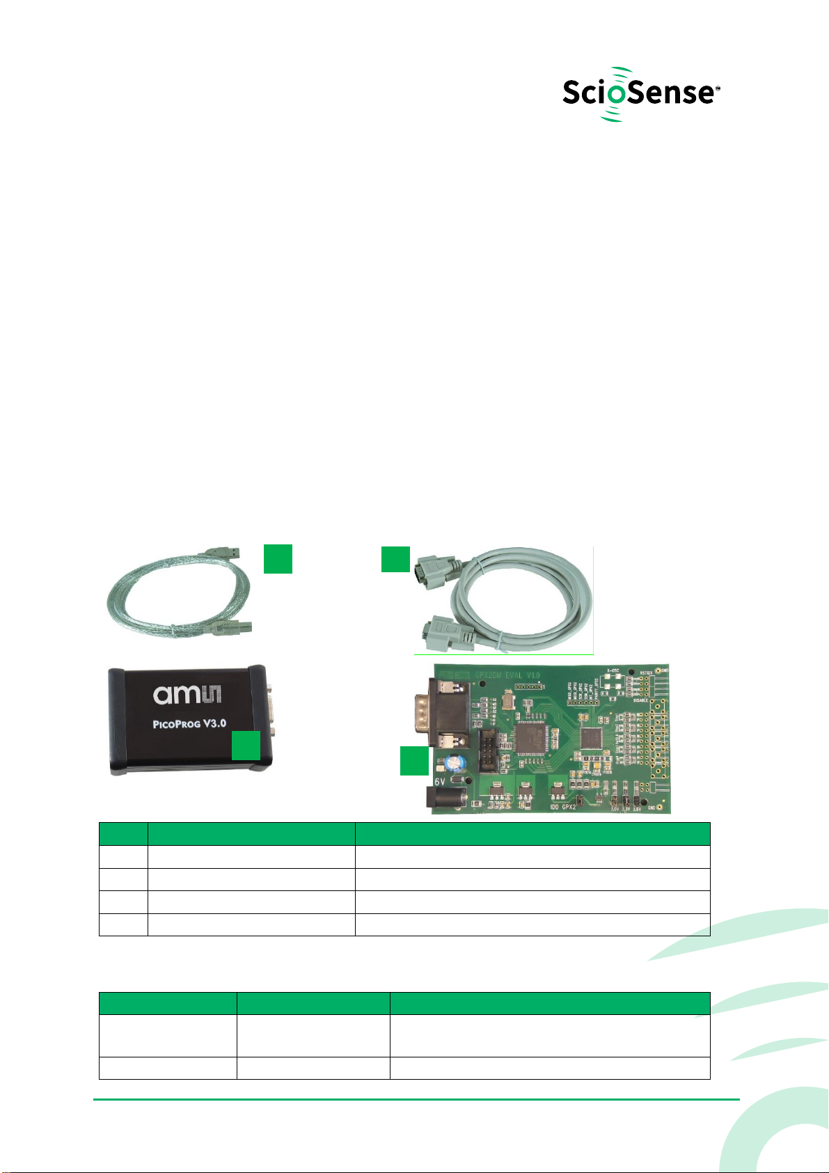
2.2 Install the Hardware: .................... 5
2.3 Software.................................. 5
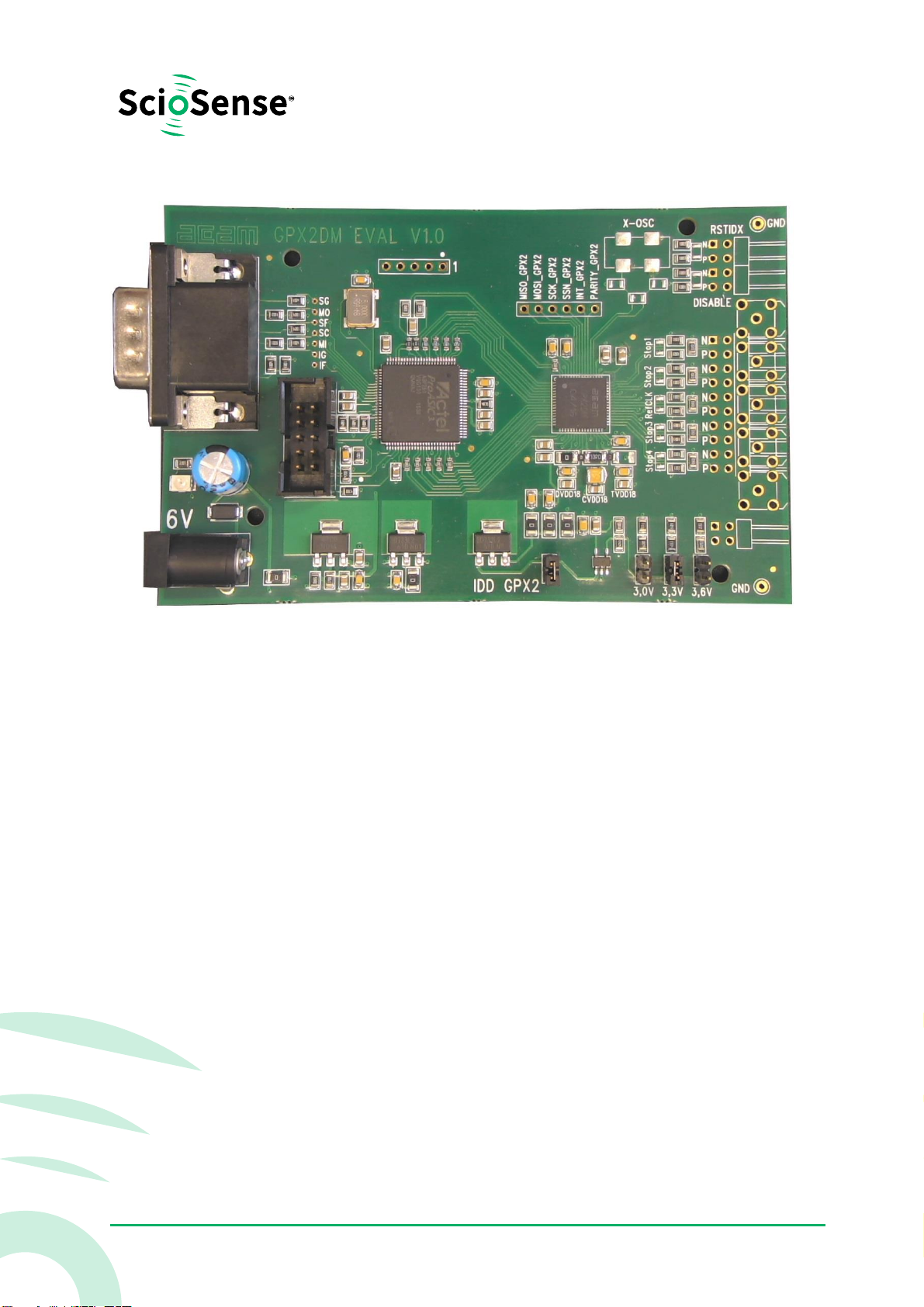
3Hardware Description ................... 5
3.1 Introduction.............................. 5
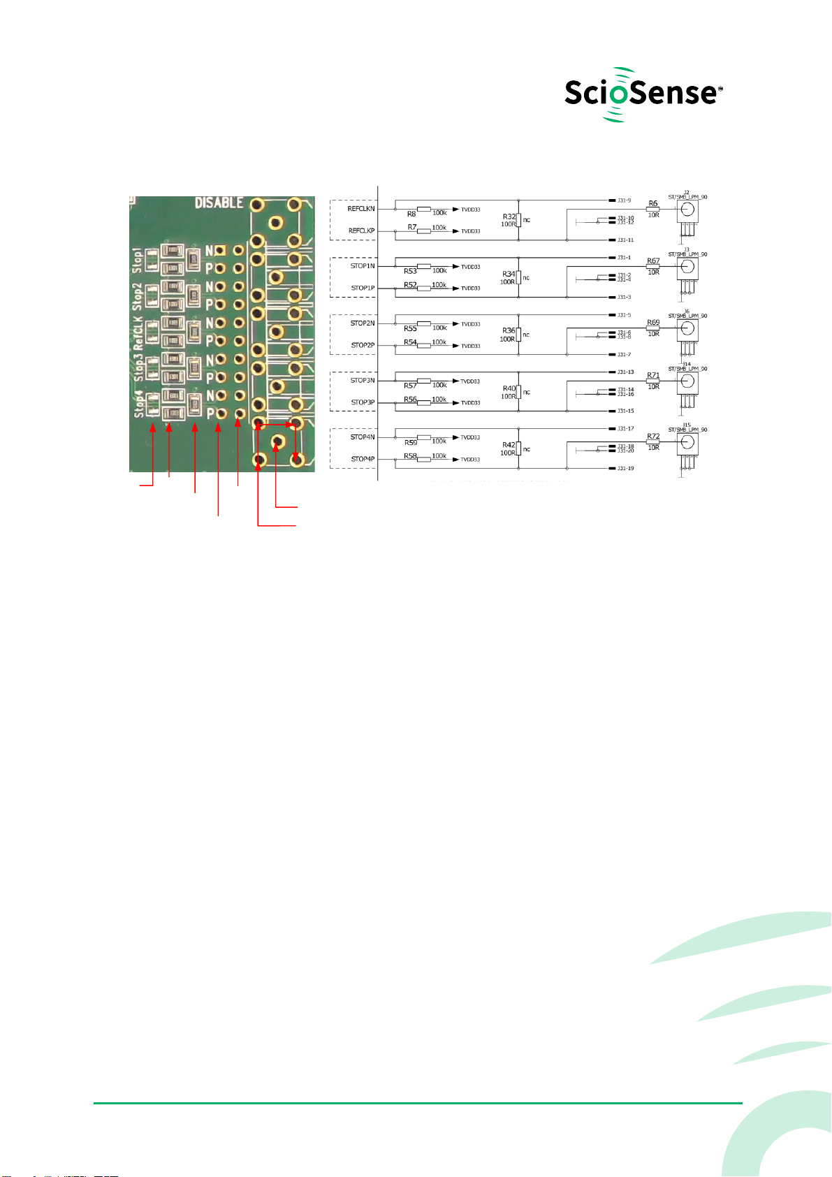
3.2 Input Signals lines ....................... 6
3.2.1 CMOS Inputs............................................ 7
3.2.2 LVDS Inputs ............................................. 7
4Software Description..................... 7
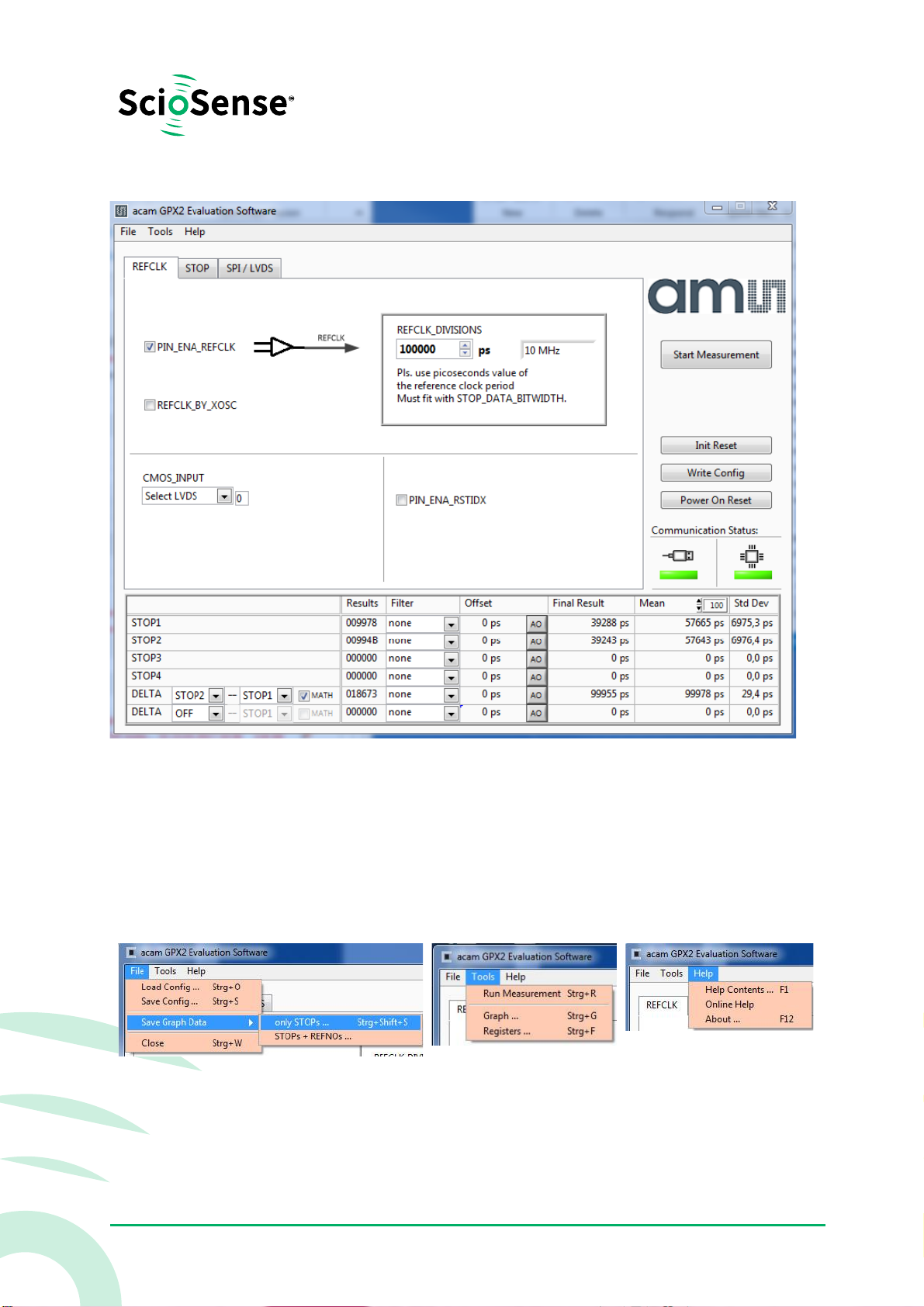
4.1 Main Window, REFCLK Page ............. 7
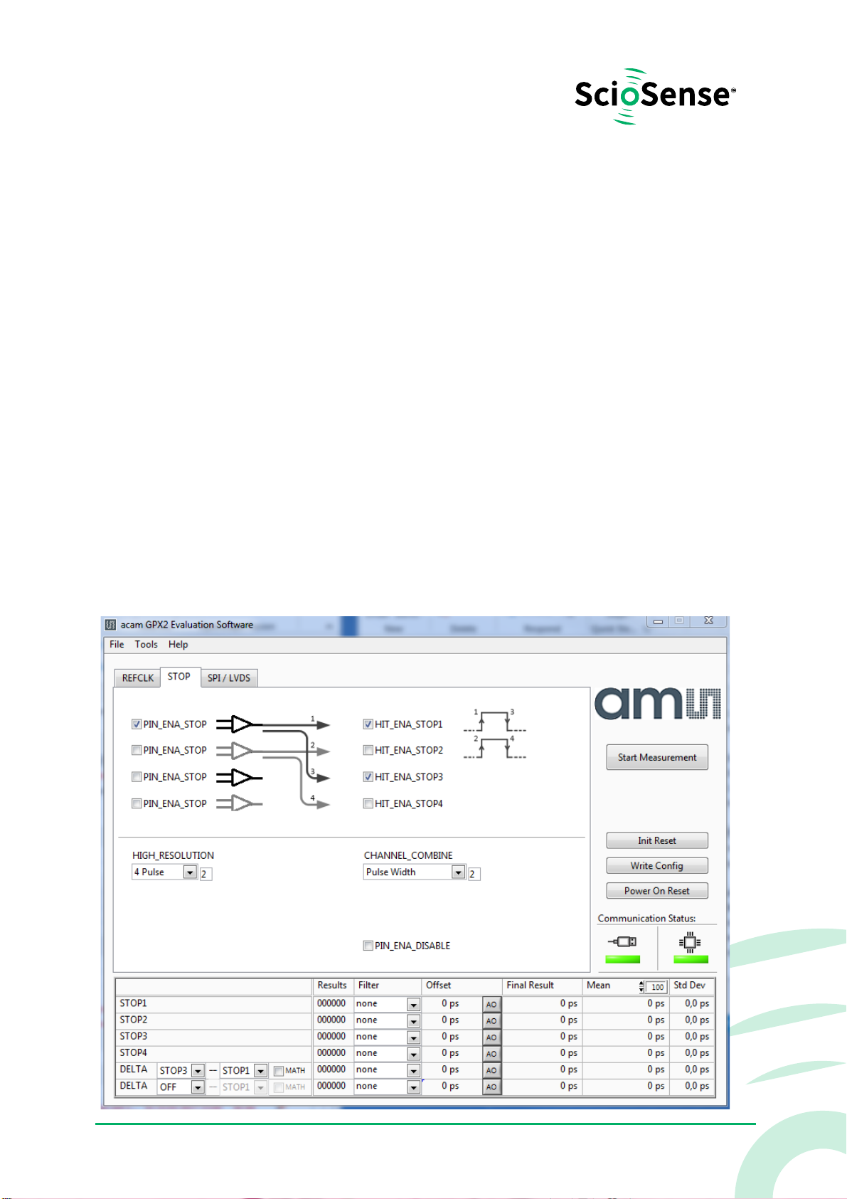
4.2 STOP Page ................................ 9
4.3 Interface Page ...........................10
4.4 Avoiding Configuration Conflicts .......10
4.5 Register Content ........................12
4.6 Graph Window...........................13
4.7 Known Errors ............................14
5Schematics, Layers and BOM ...........15
6Copyrights & Disclaimer ................22
7Document Status........................23
8Revision Information....................23

PUBLIC INFORMATION
GPX2-EVA-Kit User Guide SC-001264-UG-5 / 2021-01-25 / Product
3
1Introduction
The GPX2-EVA-KIT evaluation system is designed as a platform for a quick and easy start of
evaluation of the TDC-GPX2 time-to-digital converter. The kit offers a graphical user interface for
user-friendly configuration and extensive testing of the TDC-GPX2. For a proper use of the
evaluation system, we strongly recommended to refer to the latest TDC-GPX2 datasheet.
Features are:
•PC supported system with USB communication interface
•Easy to use evaluation and measurement software
•Different power options, selectable by jumpers
•Three reference clock sources for alternate clock options
•Data collection to ASCII text files
•Visualization of measurement results
Figure 1: Kit Content
Pos.
Item
Comment
1
PICOPROG V3.0
Programmer and interface
2
GPX2-EVA BOARD
Based on TDC-GPX2, V1.0
3
High density DSUB15 cable
Connecting Evaluation board to programmer
4
USB cable
Connects PicoProg V3.0 to PC
1.1 Ordering Information
Ordering Code
Part Number
Description
GPX2-EVA-KIT
220310001
TDC-GPX2 Eval Kit for QFN40 version including
PICOPROG and cables
GPX2-EVA-BOARD
220310003
TDC-GPX2 evaluation board for QFN64
1
2
3
4

PUBLIC INFORMATION
4
GPX2-EVA-Kit User Guide SC-001264-UG-5 / 2021-01-25 / Product
2Quick Start Guide
This section describes how to set up the GPX2-EVA-KIT, establish basic operation and make
measurements quickly.
2.1 Install the Software
Please download the latest software for the kit from:
Link: https://downloads.sciosense.com/tdc-gpx2/
It is crucial to install the software before connecting the evaluation kit to your computer. A default
driver loading of your OS may interfere with correct installation.
Figure 2: Installation steps
Step
Screen
Download the latest software installation
package to the desired directory.
Unzip the package to the desired directory.
Open “setup.exe” from the unzipped directory.
Follow the instructions on the screen.
When connecting the PicoProg to the USB port
it will be listed first as “picoprog v2.0 un-
programmed” device.
This is true also for PicoProg V3.0.
Starting the software will download a special
firmware into the PICOPROG,
picoprog_gpx2_v005.hex or higher, and the
device will now be listed as “UNIPRO”:
St Open the START Menu and open the
software from
C:\Program files\…\GPX2\GPX2 Frontpanel

PUBLIC INFORMATION
GPX2-EVA-Kit User Guide SC-001264-UG-5 / 2021-01-25 / Product
5
2.2 Install the Hardware:
•Make sure software is installed correctly before proceeding with this step!
•Connect your computer with the PicoProg V3.0 using USB cable.
•Connect PicoProg V3.0 and the evaluation kit motherboard using the DB15
interfaces or directly.
•Connect the power supply. Make sure it is set to 6 V supply voltage.
•The green LED on the evaluation kit should be on.
•Connect your signal source.
2.3 Software
•Execute the GPX2 Frontpanel Software. The communication status should be green
•The software starts with an initial configuration, that can be opened the default
configuration file config_default.cfg.
•Press “Power On Reset! – “Write Config” – “Init Reset”
•Press “Start Measurement”
The measurement should run and results should be displayed now.
3Hardware Description
3.1 Introduction
An on-board FPGA [1] manages the communication to the TDC-GPX [2]. It writes the configuration
into the chip via the SPI interface and can use the same to read data. In addition, the FPGA
manages the readout from the serial LVDS outputs of the TDC-GPX2. The SPI signals are available
via additional pads [3]. A jumper selects the supply voltage as 3.0 V, 3.3 V or 3.6 V [4]. A separate
jumper allows measuring the current into the TDC-GPX2 [5].

PUBLIC INFORMATION
6
GPX2-EVA-Kit User Guide SC-001264-UG-5 / 2021-01-25 / Product
Figure 3: GPX2-EVA-BOARD
Solder pads are prepared to apply an external oscillator. This may be used as a reference instead of
the RefClk input. [6]
Further, solder pads are available to connect the signal lines. Here the user may solder cables
directly, apply pin connectors, or in case of CMOS signals pads for SMB connectors are prepared.
Note: The FPGA manages the SPI communication and blocks the lines. Therefore, if you want to
communicate directly with TDC-GPX2 via SPI [3] then remove 0Ohm resistors R75, R76 and R77 first
[7].
3.2 Input Signals lines
The board is prepared to connect directly CMOS input signals or LVDS signals.

PUBLIC INFORMATION
GPX2-EVA-Kit User Guide SC-001264-UG-5 / 2021-01-25 / Product
7
Figure 4: Input section
CMOS In
CMOS GND
LVDS
P/N In
LVDS
GND
10R
CMOS
100k
LVDS
100R
N.c.
LVDS
3.2.1 CMOS Inputs
On the board there is a 10 Ohm series resistor.
3.2.2 LVDS Inputs
On the board there are 100kOhm pull-up resistors to TVDD33. The resistors interconnecting P and
N inputs are not assembled.
4Software Description
4.1 Main Window, REFCLK Page
The software will start with the following main window:

PUBLIC INFORMATION
8
GPX2-EVA-Kit User Guide SC-001264-UG-5 / 2021-01-25 / Product
Figure 5: GPX2 evaluation software main window
The main menu offers the typical functions to load and save configurations, to run a measurement,
to open the graph and register windows as well as a help.
The two figures on the right indicate the communication status. Both bar indicators should be
green.
Figure 6: Menu selections
As a first step we recommend to load the standard configuration config_default.cfg, then press
“Power On Reset”, “Write Config” and “Init Reset”.
The first page, “REFCLK”, allows the user to select the reference input as well as the definition of
the LSB. REFCLK_DIVISIONS defines the LSB at the output interface as fraction of the reference

PUBLIC INFORMATION
GPX2-EVA-Kit User Guide SC-001264-UG-5 / 2021-01-25 / Product
9
clock period. The most convenient way is applying an LSB of 1ps by configuring REFCLK_DIVISIONS
to the picosecond value of the reference clock period.
In the middle section the user selects between CMOS and LVDS.
At the bottom, visible on all tabulators, is the numerical display of the measurement results STOP1
to STOP2. In addition, the software allows to calculate the difference between two stop results.
The select box “Math” defines the formula:
Calculation Formula:
•On: [STOP1 - STOP2]
•Off: [REFNO1 - REFNO2] * REFCLK_DIVISIONS + [STOP1 - STOP2]
Various software filters, sinc or median, can be applied.
4.2 STOP Page
This page is for the PIN and HIT enable selection as well as the high resolution and combined
channel settings.
Figure 7: STOP page

PUBLIC INFORMATION
10
GPX2-EVA-Kit User Guide SC-001264-UG-5 / 2021-01-25 / Product
4.3 Interface Page
On this page the communication as well as the output data format is defined. In any case, on the
evaluation kit all communication is done via the on-board FPGA.
Figure 8: Interface page
Note: The read out speed of the evaluation software is much less than the TDC sample rate.
Therefore, in most cases BLOCKWISE_FIFO_READ will give more reasonable display. In addition,
often the difference between channels is of interest only and DELTA should be used for display. To
have this calculated correctly, Math should be enabled.
COMMOM_FIFO_READ helps if the same number of data from several channels is expected.
4.4 Avoiding Configuration Conflicts
Some combinations of parameter settings can prohibit operation or cause erroneous results. Some
of these combinations are indicated with a red bar. User should avoid such configurations since
the results may be difficult to interpret or faulty at all.
Some examples of configuration conflicts:

PUBLIC INFORMATION
GPX2-EVA-Kit User Guide SC-001264-UG-5 / 2021-01-25 / Product
11
Figure 9: Avoiding conflicts
A
Bad
Good
B
Bad
Good
C
Bad
Good
D
Bad
Good
E
The LVDS readout frequency is recommended
up to 360MHz in SDR mode only. Nevertheless
400 MHz is possible to configure and operate

PUBLIC INFORMATION
12
GPX2-EVA-Kit User Guide SC-001264-UG-5 / 2021-01-25 / Product
4.5 Register Content
A separate window shows the register content in the GUI and the TDC-GPX2. Separate pages
display configuration data and result data. Changing the hexadecimal values will change the
configuration in the GUI accordingly. With “Write Config” the updated configuration is downloaded
into the chip.
Figure 10: Registers Window: Configuration
Figure 11: Registers Window: Results

PUBLIC INFORMATION
GPX2-EVA-Kit User Guide SC-001264-UG-5 / 2021-01-25 / Product
13
4.6 Graph Window
The graphical display allows to select which data shall be displayed. The shape of the individual
curves can be modified individually. Move the mouse over the line symbol and press the right mouse
button. A menu with many options will pop up.
There are dedicated buttons for zoom to all or zoom in X or Y only. In addition, the standard Labview
zoom functions are available (see the icons on the top right).
Figure 12: Graph Window
The displayed data can be exported into a text file. The maximum is 128,000 data sets.
Figure 13: Save data menu
The text file can then be analyzed with a table calculation program.

PUBLIC INFORMATION
14
GPX2-EVA-Kit User Guide SC-001264-UG-5 / 2021-01-25 / Product
Figure 14: Exported data format
4.7 Known Errors
•Software Hang-up
oOccasionally, typically during tests in the temperature chamber, it may
happen that the software hangs up. This is most likely to erroneous
reading from the FIFO and related in the FPGA. The error will be
removed in the next revision of the FPGA.

PUBLIC INFORMATION
GPX2-EVA-Kit User Guide SC-001264-UG-5 / 2021-01-25 / Product
15
5Schematics, Layers and BOM
Figure 15: GPX2-EVA BOARD Schematics 1

PUBLIC INFORMATION
16
GPX2-EVA-Kit User Guide SC-001264-UG-5 / 2021-01-25 / Product
Figure 16: GPX2-EVA BOARD Schematics 2

PUBLIC INFORMATION
GPX2-EVA-Kit User Guide SC-001264-UG-5 / 2021-01-25 / Product
17
Figure 17: GPX2-EVA BOARD Schematics 3

PUBLIC INFORMATION
18
GPX2-EVA-Kit User Guide SC-001264-UG-5 / 2021-01-25 / Product
Figure 18: GPX2-EVA BOARD Layout: Top layer
Figure 19: GPX2-EVA BOARD Layout: GND Layer

PUBLIC INFORMATION
GPX2-EVA-Kit User Guide SC-001264-UG-5 / 2021-01-25 / Product
19
Figure 20: GPX2-EVA BOARD Layout: VDD Layer
Figure 21: GPX2-EVA BOARD Layout: Bottom layer

PUBLIC INFORMATION
20
GPX2-EVA-Kit User Guide SC-001264-UG-5 / 2021-01-25 / Product
Figure 22: GPX2-EVA BOARD Layout: Assembly layer
Figure 23: Bill of Materials for GPX2-EVA BOARD
QTY
DESIGNATOR
VALUE
PART DESC
TYPE
1
C5
10n
CHIP-CAPACITOR 0805
17
C2 C6 C7 C11 C14 C16
C17 C18 C20 C21 C22
C30 C33 C45 C46 C56
C57
100n
CHIP-CAPACITOR 0805
11
C3 C8 C12 C15 C19 C23
C29 C31 C43 C49 C60
33u
TANTAL
F950J336MPAAQ2
2
C9 C13
100u
TANTAL
F950J107MPAAQ2
1
C32
220u
TANTAL
F950J227MBAAM1Q2
1
C1
330u/25V
ELECTROLYTIC
CAPASITOR
Radial 8mm Raster
2,5mm
10
R2 R16 R22 R23 R24
R25 R26 R27 R33 R35
100R
CHIP-RESISTOR 0603
2
R30 R31
165R
CHIP-RESISTOR 0603
3
R75 R76 R77
0R
CHIP-RESISTOR 0805
1
R49
4R7
CHIP-RESISTOR 0805
5
R6 R67 R69 R71 R72
10R
CHIP-RESISTOR 0805
1
R45
56R
CHIP-RESISTOR 0805
2
R17 R28
68R
CHIP-RESISTOR 0805
2
R10 R51
100R
CHIP-RESISTOR 0805
This manual suits for next models
1
Table of contents