Seiko Epson S5U13L02P00C100 User manual

Rev. 1.1
S1D13L02 LCD controller
S5U13L02P00C100 Evaluation
Board User Manual
Document Number: XB0A-G-001-01.1

NOTICE
No part of this material may be reproduced or duplicated in any form or by any means without the written permission
of Seiko Epson. Seiko Epson reserves the right to make changes to this material without notice. Seiko Epson does
not assume any liability of any kind arising out of any inaccuracies contained in this material or due to its application
or use in any product or circuit and, further, there is no representation that this material is applicable to products
requiring high level reliability, such as, medical products. Moreover, no license to any intellectual property rights
is granted by implication or otherwise, and there is no representation or warranty that anything made in accordance
with this material will be free from any patent or copyright infringement of a third party. When exporting the
products or technology described in this material, you should comply with the applicable export control laws and
regulations and follow the procedures required by such laws and regulations. You are requested not to use, to resell,
to export and/or to otherwise dispose of the products (and any technical information furnished, if any) for the devel-
opment and/or manufacture of weapon of mass destruction or for other military purposes.
All brands or product names mentioned herein are trademarks and/or registered trademarks of their respective
companies.
©SEIKO EPSON CORPORATION 2014-2018. All rights reserved.
Evaluation Board/Kit and Development Tool Important Notice
1. This evaluation board/kit or development tool is designed for use for engineering evaluation, demonstration, or develop-
ment purposes only. Do not use it for other purposes. It is not intended to meet the requirements of design for finished
products.
2. This evaluation board/kit or development tool is intended for use by an electronics engineer and is not a consumer product.
The user should use it properly and in a safe manner. Seiko Epson does not assume any responsibility or liability of any
kind of damage and/or fire caused by the use of it. The user should cease to use it when any abnormal issue occurs even
during proper and safe use.
3. The part used for this evaluation board/kit or development tool may be changed without any notice.
2Seiko Epson Corporation S5U13L02P00C100 Evaluation Board
Rev. 1.1

S5U13L02P00C100 Evaluation Board Seiko Epson Corporation 3
Rev. 1.1
Table of Contents
Chapter 1 Introduction . . . . . . . . . . . . . . . . . . . . . . . . . . . . . . . . . . . . 5
Chapter 2 Features . . . . . . . . . . . . . . . . . . . . . . . . . . . . . . . . . . . . . . 6
Chapter 3 Installation and Configuration . . . . . . . . . . . . . . . . . . . . . . . . . . 7
3.1 Configuration DIP Switch . . . . . . . . . . . . . . . . . . . . . . . . . . . 7
3.2 Configuration Jumpers . . . . . . . . . . . . . . . . . . . . . . . . . . . . 8
Chapter 4 Technical Description . . . . . . . . . . . . . . . . . . . . . . . . . . . . . 12
4.1 Power . . . . . . . . . . . . . . . . . . . . . . . . . . . . . . . . . 12
4.1.1 Power Requirements . . . . . . . . . . . . . . . . . . . . . . . . . . . . . . . . . 12
4.1.2 Voltage Regulators . . . . . . . . . . . . . . . . . . . . . . . . . . . . . . . . . . 12
4.1.3 S1D13L02 Power . . . . . . . . . . . . . . . . . . . . . . . . . . . . . . . . . . . 12
4.2 Clocks . . . . . . . . . . . . . . . . . . . . . . . . . . . . . . . . . 13
4.3 Reset . . . . . . . . . . . . . . . . . . . . . . . . . . . . . . . . . . 13
4.4 Host Interface . . . . . . . . . . . . . . . . . . . . . . . . . . . . . . 14
4.4.1 Direct Host Bus Interface Support . . . . . . . . . . . . . . . . . . . . . . . . . . 14
4.4.2 Connecting to the Epson S5U13U00P00C100 USB Adapter Board . . . . . . . . . 15
4.5 LCD Panel Interface . . . . . . . . . . . . . . . . . . . . . . . . . . . . 16
4.6 GPIO Connections . . . . . . . . . . . . . . . . . . . . . . . . . . . . 17
Chapter 5 Parts List . . . . . . . . . . . . . . . . . . . . . . . . . . . . . . . . . . . . 18
Chapter 6 Schematic Diagrams . . . . . . . . . . . . . . . . . . . . . . . . . . . . . . 20
Chapter 7 Board Layout . . . . . . . . . . . . . . . . . . . . . . . . . . . . . . . . . . 23
Chapter 8 Change Record . . . . . . . . . . . . . . . . . . . . . . . . . . . . . . . . . 25
Chapter 9 Sales and Technical Support . . . . . . . . . . . . . . . . . . . . . . . . . 26

4Seiko Epson Corporation S5U13L02P00C100 Evaluation Board
Rev. 1.1

Introduction
S5U13L02P00C100 Evaluation Board Seiko Epson Corporation 5
Rev. 1.1
Chapter 1 Introduction
This manual describes the setup and operation of the S5U13L02P00C100 Evaluation Board. The evaluation board
is designed as an evaluation platform for the S1D13L02 LCD controller.
The S5U13L02P00C100 Evaluation Board can also connect to the S5U13U00P00C100 USB Adapter board so that
it can be used with a laptop or desktop computer, via USB 2.0. The S5U13L02P00C100 Evaluation Board can be
used with many native platforms via the host connector which provides the appropriate signals to support a variety
of CPUs. However, if you do not use the S5U13U00P00C100 USB Adapter board, there are no headers mounted
for the other host interfaces. (there are unpopulated spaces allocated for headers.) Please use the allocated space to
mount the headers to use other host interfaces.
This document is updated as appropriate. Please check for the latest revision of this document before beginning any
development. The latest revision can be downloaded at vdc.epson.com.
We appreciate your comments on our documentation. Please contact us via email at
vdc-document[email protected].com.

Features
6Seiko Epson Corporation S5U13L02P00C100 Evaluation Board
Rev. 1.1
Chapter 2 Features
The S5U13L02P00C100 Evaluation Board includes the following features:
• 208-pin QFP22 S1D13L02 LCD controller
• Headers for connection to the S5U13U00P00C100 USB Adapter board
• Header with all S1D13L02 Host Bus Interface signals (optional)
Note
These headers are not mounted. There are allocated spaces for the headers.
• Headers for connecting to LCD panels
• Header for S1D13L02 GPIO pins (optional)
Note
These headers are not mounted. There are allocated spaces for the headers.
• On-board 4MHz oscillator
• 3.3V input power
• On-board voltage regulator with 1.5V output
• On-board voltage regulator with adjustable 38V/60mA max, to provide power for LED back-light of LDC
panels.
Installation and Configuration
S5U13L02P00C100 Evaluation Board Seiko Epson Corporation 7
Rev. 1.1
Chapter 3 Installation and Configuration
The S5U13L02P00C100 Evaluation Board incorporates a DIP switch, jumpers, and 0 ohm resistors which allow it
to be used with a variety of different configurations.
3.1 Configuration DIP Switch
The S1D13L02 has 2 configuration inputs (CNF[2:1]). A DIP switch (SW1) is used to configure CNF[2:1] as
described below.
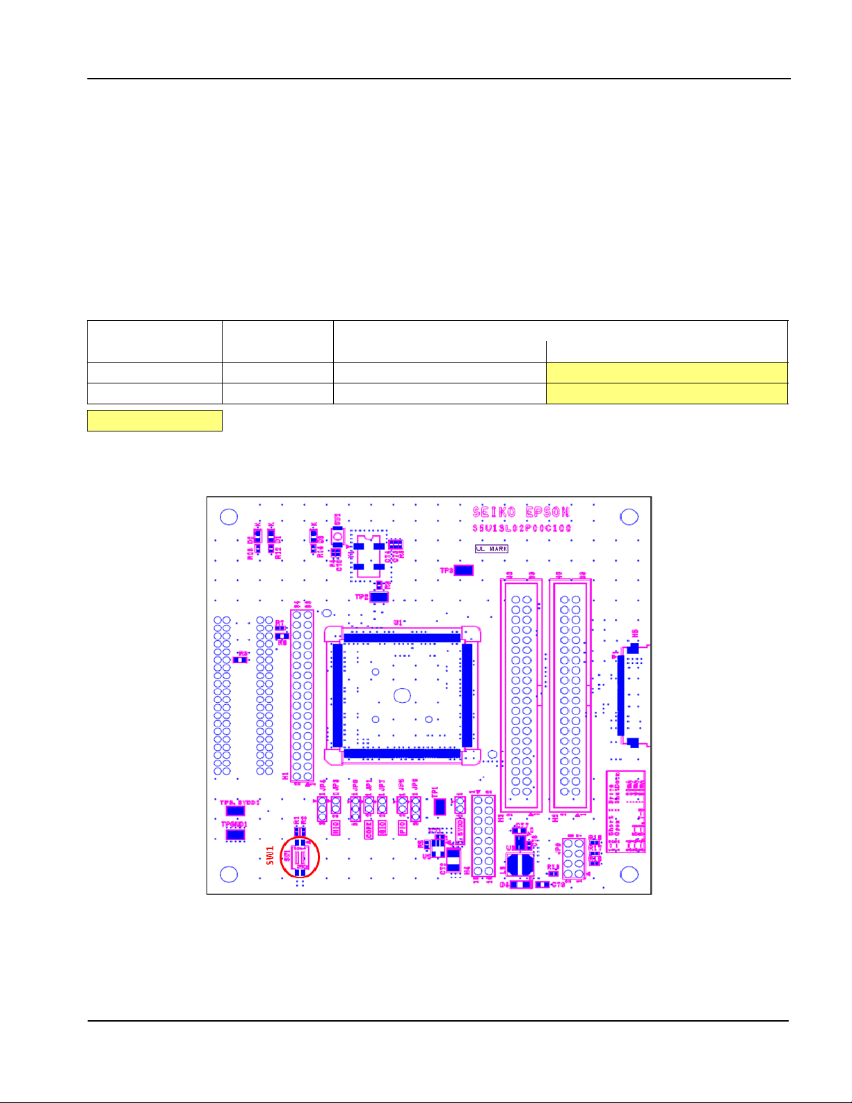
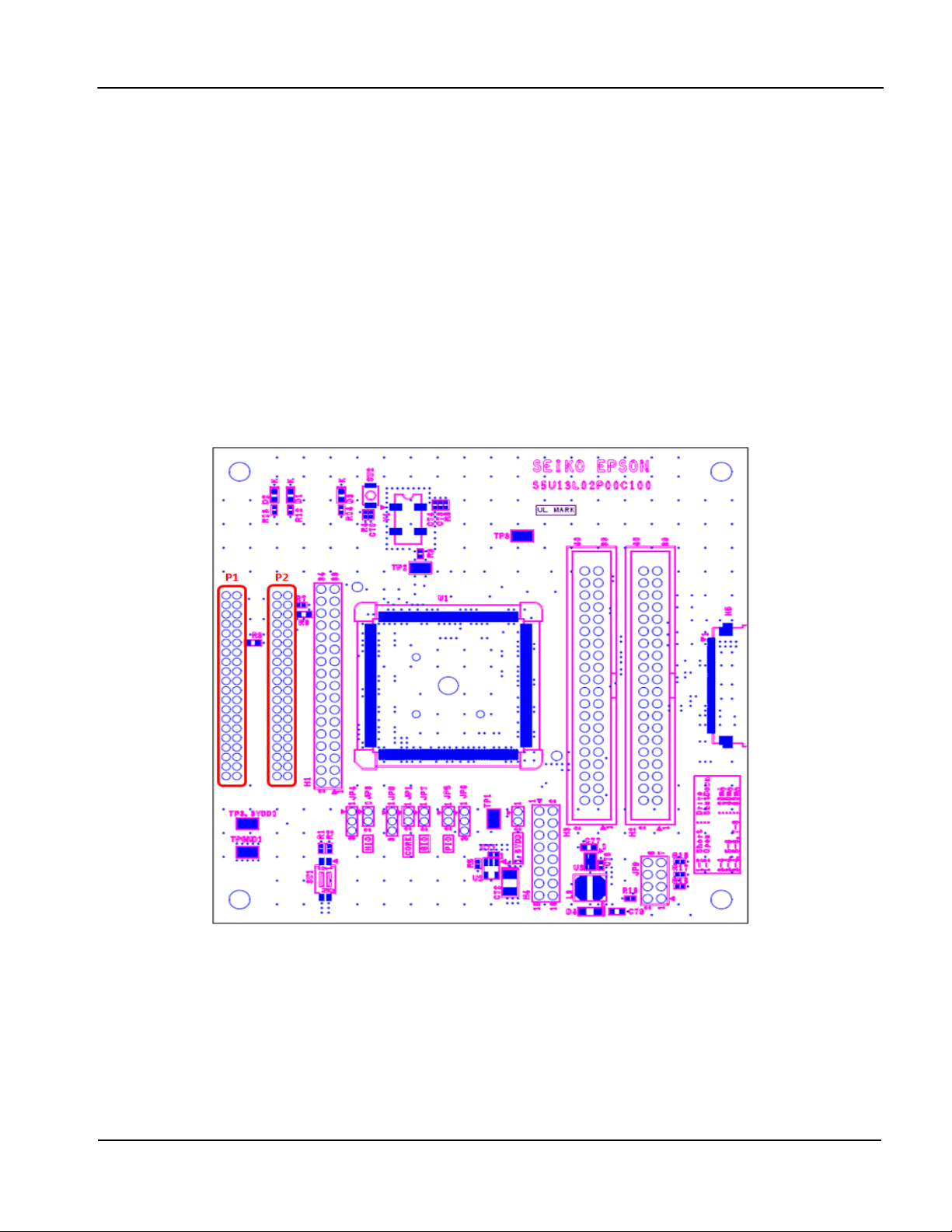
The following figure shows the location of DIP switch SW1 on the S5U13L02P00C100 Evaluation Board.
Figure 3-1: Configuration DIP Switch (SW1) Location
Table 3-1: Configuration DIP Switch Settings
S5U13L02P00C100
SW1-[2:1] Config
S1D13L02
CNF[2:1] Config
Power-On/Reset State
1 (ON) 0 (OFF)
SW1-[2] CNF2 Big Endian Little Endian
SW1-[1] CNF1 Indirect 68 Indirect 80
= Required settings when using S5U13U00P00C100 USB Adapter board

Installation and Configuration
8Seiko Epson Corporation S5U13L02P00C100 Evaluation Board
Rev. 1.1
3.2 Configuration Jumpers
The S5U13L02P00C100 Evaluation Board has 2-pin jumpers (x 8) which configure various board settings. And this
board has 8-pin jumper for setting backlight of the LCD panel. The jumper positions for each function are shown
below.
Table 3-3: 8-PinJumper Setting
Table 3-2: Configuration Jumper Settings
Jumper Function Position 1-2 Position 2-3 No Jumper
JP1 COREVDD Normal —COREVDD current
measurement
JP2 PLLVDD Normal —PLLVDD current
measurement
JP3 HIOVDD Normal —HIOVDD current
measurement
JP4 HIOVDD Source H1 connector, pin 32 3.3VDD —
JP5 PIOVDD Normal —PIOVDD current
measurement
JP6 PIOVDD Source H4 connector, pin 2 3.3VDD —
JP7 GIOVDD Normal —GIOVDD current
measurement
JP8 GIOVDD Source H4 connector, pin 6 3.3VDD —
= Required settings when using S5U13U00P00C100 USB Adapter board
Jumper Position Function
JP9
Position 1-2 No Jumper In connect case, TPS61161A is Enable
Position 3-4 No Jumper In connect case, Vout = 20mA
Position 5-6 No Jumper In connect case, Vout = 40mA (add connect Position 3-4)
Position 7-8 No Jumper In connect case, Vout = 60mA (add connect Position3-4 and
Position5-6)
= suggested settings
Installation and Configuration
S5U13L02P00C100 Evaluation Board Seiko Epson Corporation 9
Rev. 1.1
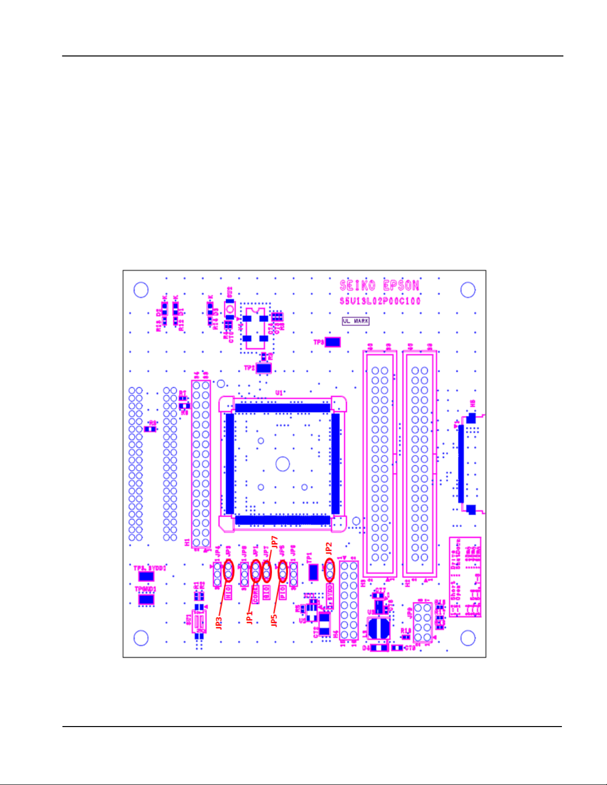
JP1, JP2, JP3, JP5, JP7 - Power Supplies for the S1D13L02
JP1, JP2, JP3, JP5, and JP7 can be used to measure the current consumption of each S1D13L02 power supply.
When the jumper is at position 1-2, normal operation is selected.
When no jumper is installed, the current consumption for each power supply can be measured by connecting an
ammeter to pin 1 and 2 of the jumper.
The jumper associated with each power supply is as follows:
JP1 for COREVDD
JP2 for PLLVDD
JP3 for HIOVDD
JP5 for PIOVDD
JP7 for GIOVDD
Figure 3-2: Configuration Jumper Locations (JP1, JP2, JP3, JP5, JP7)

Installation and Configuration
10 Seiko Epson Corporation S5U13L02P00C100 Evaluation Board
Rev. 1.1
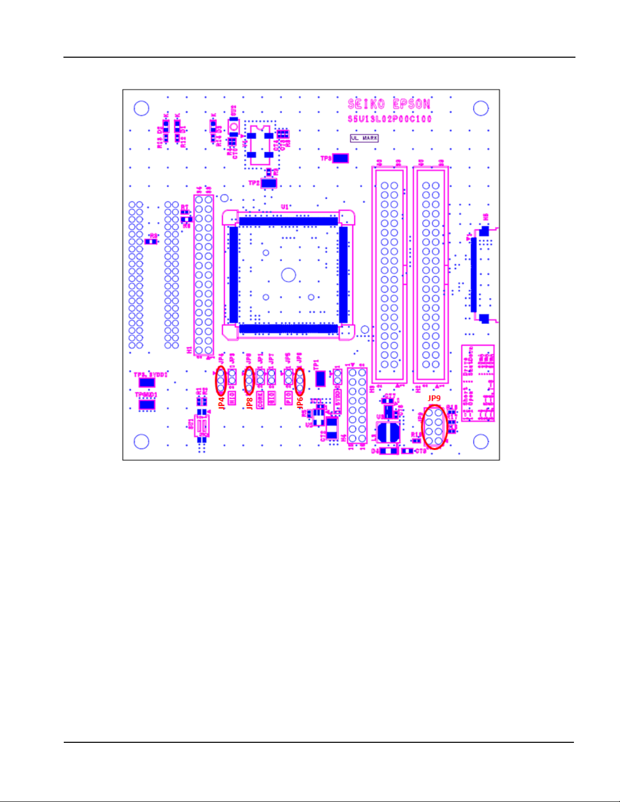
JP4 - HIOVDD Source
JP4 is used to select the source for the HIOVDD supply voltage.
When the jumper is at position 1-2, the HIOVDD voltage must be provided to pin 32 on the H1 connector.
When the jumper is at position 2-3, the HIOVDD voltage is provided by the 3.3V power supply of the board.
Note
HI connector is not mounted. There is allocated space for the connector.
JP6 - PIOVDD Source
JP6 is used to select the source for the PIOVDD supply voltage.
When the jumper is at position 1-2, the PIOVDD voltage must be provided to pin 2 on the H4 connector.
When the jumper is at position 2-3, the PIOVDD voltage is provided by the 3.3V power supply of the board.
Note
H4 connector is not mounted. There is allocated space for the connector.
JP8 - GIOVDD Source
JP8 is used to select the source for the GIOVDD supply voltage.
When the jumper is at position 1-2, the GIOVDD voltage must be provided to pin 6 on the H4 connector.
When the jumper is at position 2-3, the GIOVDD voltage is provided by the 3.3V power supply of the board.
Note
H4 connector is not mounted. There is allocated space for the connector.
JP9 - Backlight Power Supply for LCD Panel
The S5U13L02P00C100 Evaluation Board is designed to generate backlight power supply for LCD panel from 3.3V
via the S5U13U00P00C100 USB adapter board or connector H1. The 3.3V must be supplied from the
S5U13U00P00C100 or H1. The S5U13L02P00C100 has incorporated the White LED Driver Controller
(TPS61161A) for the panel backlight. The White LED Driver Controller drives the panel at a constant current. The
S5U13L02P00C100 is capable of changing the output current (20mA, 40mA, 60mA/Max38V).The current is
adjusted by connection of JP9.See Table 3.3: 8-pin jumper setting”“
Note
H1 connector is not mounted. There is allocated space for the connector.
Installation and Configuration
S5U13L02P00C100 Evaluation Board Seiko Epson Corporation 11
Rev. 1.1
Figure 3-3: Configuration Jumper Location (JP4, JP6, JP8, JP9)

Technical Description
12 Seiko Epson Corporation S5U13L02P00C100 Evaluation Board
Rev. 1.1
Chapter 4 Technical Description
4.1 Power
4.1.1 Power Requirements
The S5U13L02P00C100 Evaluation Board requires an external regulated power supply (3.3V / 1A). The power is
supplied to the evaluation board through pin 34 of the H1 header, or pin 5 of the P2 header.
The green LED “3.3V Power” is turned on when 3.3V power is applied to the board.
Note
H1 connector is not mounted. There is allocated space for the connector.
4.1.2 Voltage Regulators
The S5U13L02P00C100 Evaluation Board has an on-board linear regulator to provide the 1.5V power required by
the S1D13L02 LCD controller. It also has a step-up switching voltage regulator to generate adjustable 12~38V,
which can be used to power the LED backlight on some LCD panels.
4.1.3 S1D13L02 Power
The S1D13L02 LCD controllerrequires 1.5V and 1.65~3.6V power supplies.
1.5V power for COREVDD and PLLVDD is provided by an on-board linear voltage regulator.
HIOVDD range of S1D13L02 isfrom 1.65V to 3.6V. However, HIOVDD of the S5U13L02P00C100 Evaluation
Board can range from 3.0V to 3.6V. When JP4 is set to the 2-3 position, HIOVDD is connected to 3.3V. If a different
voltage is required for HIOVDD, set JP4 to the 1-2 position and connect the external power supply to pin 32 of
connector H1.
Note
H1 connector is not mounted. There is allocated space for the connector.
PIOVDD of S1D13L02 is the power used by the LCD interface and GPIO[23:8] and can range from 1.65V to 3.6V.
However, PIOVDD of the S5U13L02P00C100 Evaluation Board can range from 3.0V to 3.6V. When JP6 is set to
the 2-3 position, PIOVDD is connected to 3.3V. If a different voltage is needed for PIOVDD because of the LCD
panel requirements, set JP6 to the 1-2 position and connect the external power supply to pin 2 of connector H4.
Note
H4 connector is not mounted. There is allocated space for the connector.
GIOVDD of S1D13L02 is the power used by GPIO[7:0] and can range from 1.65V to 3.6V. However, PIOVDD of
the S5U13L02P00C100 Evaluation Board can range from 3.0V to 3.6V. When JP8 is set to the 2-3 position,
GIOVDD is connected to 3.3V. If a different voltage is needed for GIOVDD, set JP8 to the 1-2 position and connect
the external power supply to pin 6 of connector H4.

Technical Description
S5U13L02P00C100 Evaluation Board Seiko Epson Corporation 13
Rev. 1.1
Note
H4 connector is not mounted. There is allocated space for the connector.
4.2 Clocks
The clock for the S1D13L02 LCD controlleris provided by a 4MHz oscillator.
Note
The on-board 4MHz oscillator is not specified to work below a 3.0V supply voltage.
4.3 Reset
The S1D13L02 LCD controlleron the S5U13L02P00C100 Evaluation Board can be reset using a push-button switch
(SW2), or via an active low reset signal from the host development platform (pin 33 on the H1 connector).
Note
H1 connector is not mounted. There is allocated space for the connector.
Figure 4-1: Reset Switch (SW2)
Technical Description
14 Seiko Epson Corporation S5U13L02P00C100 Evaluation Board
Rev. 1.1
4.4 Host Interface
4.4.1 Direct Host Bus Interface Support
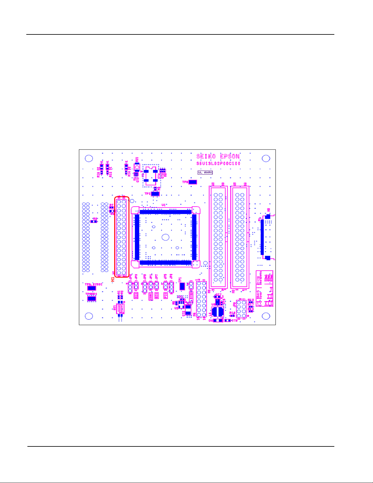
All S1D13L02 host interface pins are available on connector H1 which allows the S5U13L02P00C100 Evaluation
Board to be connected to a variety of development platforms. For detailed S1D13L02 pin mapping, refer to the
S1D13L02 Hardware Functional Specification, document number XB0AA001.
The following figure shows the location of host bus connector H1. H1 is not mounted. H1 connector is optional.
There is allocated space for the connector. If to use this allocated space , it is recommended to attach the 0.1 inch x
0.1 inch, 34-pin header (17 x 2).
Figure 4-2: Host Bus Connector Location (H1)
For the pinout of connector H1, see Section Chapter 6, “Schematic Diagrams” on page 20.
Technical Description
S5U13L02P00C100 Evaluation Board Seiko Epson Corporation 15
Rev. 1.1
4.4.2 Connecting to the Epson S5U13U00P00C100 USB Adapter Board
The S5U13L02P00C100 Bvaluation Board is designed to connect to a S5U13U00P00C100 USB Adapter Board.
The USB adapter board provides a simple connection to any computer via a USB 2.0 connection. The
S5U13L02P00C100 directly connects to the USB adapter board through connectors P1 and P2.
The USB adapter board also supplies the 3.3V power required by the S5U13L02P00C100. HIOVDD should be
selected for 3.3V and JP4 should be set to the 2-3 position.
When the S5U13L02P00C100 is connected to the S5U13U00P00C100 USB Adapter board, there are 2 LEDs on
the S5U13L02P00C100 which provide a quick visual status of the USB adapter. HB (D300)blinks to indicate that
the USB adapter board is active. ENUM (D301)turns on to indicate that the USB has been enumerated by the PC.
The following diagram shows the location of connectors P1 and P2. P1 and P2 are 2mm x 2mm, 40-pin headers
(20 x 2).
Figure 4-3: USB Adapter Connector Locations (P1 and P2)
For the pinout of connectors P1 and P2, see Section Chapter 6, “Schematic Diagrams” on page 20.
Note
A windows driver must be installed on the PC when the S5U13L02P00C100 is used with the S5U13U00P00C100
USB Adapter Board. The S1D13xxxUSB driver is available vdc.epson.com.

Technical Description
16 Seiko Epson Corporation S5U13L02P00C100 Evaluation Board
Rev. 1.1
4.5 LCD Panel Interface
The LCD interface signals are available on connectors H2, H3 and H5.
For S1D13L02 LCD interface pin mapping, refer to the S1D13L02 Hardware Functional Specification, document
number XB0A-A-001.
Connectors H2and H3 are 0.1” x 0.1”, 40-pin headers (20 x 2). Connector H5 is 0.5mm pitch, 40-pin FPC connector.
The following diagram shows the location of connectors H2, H3,and H5.
Note
Connector H2 and H3 are not mounted. H2 and
Figure 4-4: LCD Panel Connectors Location (H2, H3, H4)
For the pinout of connectors H2, H3,H4 and H5, see Section Chapter 6, “Schematic Diagrams” on page 20.

Technical Description
S5U13L02P00C100 Evaluation Board Seiko Epson Corporation 17
Rev. 1.1
4.6 GPIO Connections
The S1D13L02 LCD controllerhas 24 GPIO pins. The GPIO[23:8] pins have dual functions and are selectable
between a LCD output or GPIO function. They are powered from PIOVDD. For S1D13L02 LCD interface pin
mapping, refer to the S1D13L02 Hardware Functional Specification, document number
XB0A-A-001.
The GPIO[7:0] pins only function as GPIOs and are powered from GIOVDD. All the GPIO pins are available on
the H3 and H4 connectors. Note that connector H4 is not populated on the S5U13L02P00C100 Evaluation Board.
Connector H3 is a 0.1” x 0.1”, 40-pin header and connector H4 is a 0.1” x 0.1”, 16-pin header (8 x 2). The following
figure shows the location of the connector H3 and H4.
Note
Connector H3 and H4 are not mounted. There is only allocated sapce for the connectors. H3 and
Figure 4-5: GPIO Connector Location (H3, H4)
For the pinout of connector H3 and H4, see Section Chapter 6, “Schematic Diagrams” on page 20.
Parts List
18 Seiko Epson Corporation S5U13L02P00C100 Evaluation Board
Rev. 1.1
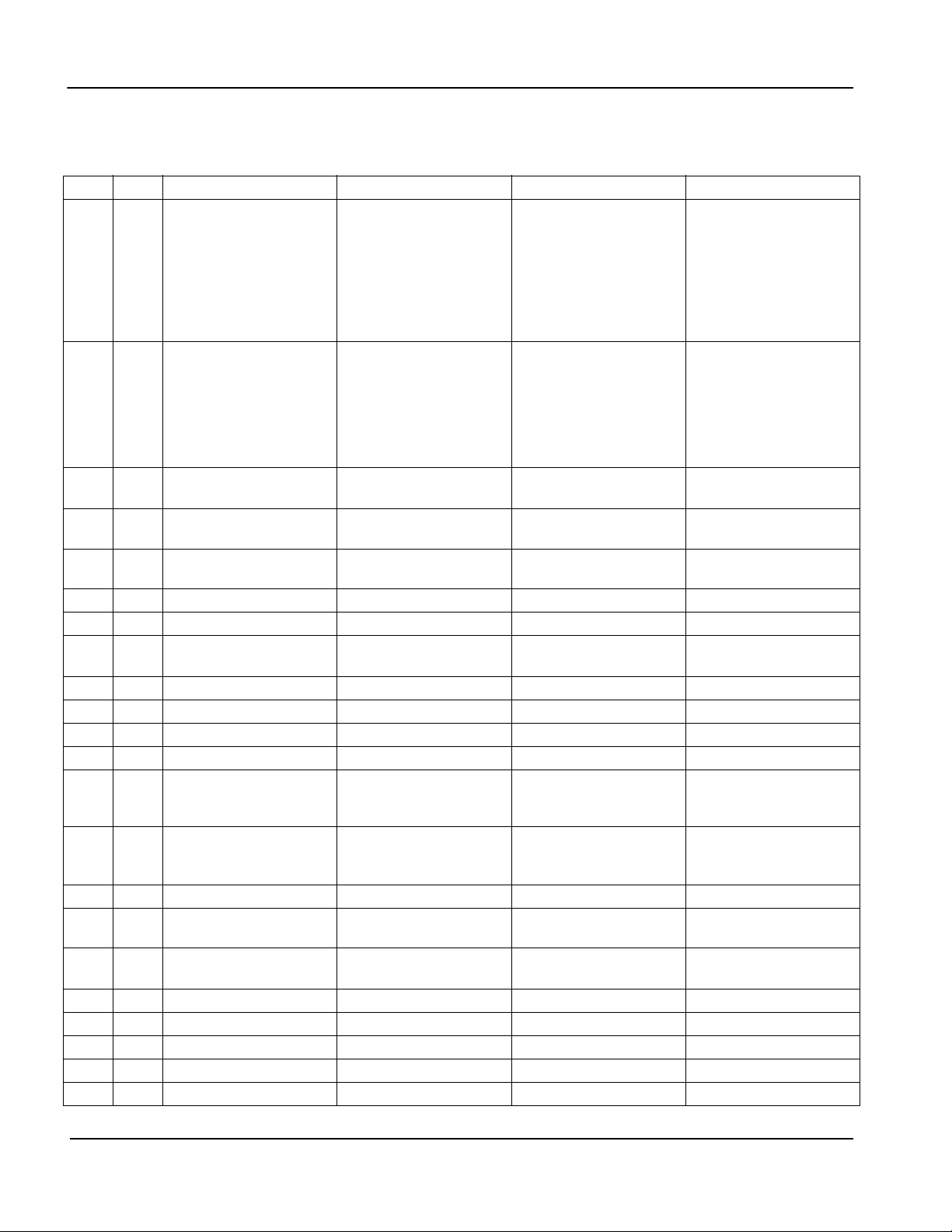
Chapter 5 Parts List
Table 5-1: S5U13L02P00C100 Parts List
Item Qty Reference Part Description Manufacturer Part No
138
C1, C2, C3, C4, C5, C6,
C7, C8, C9, C10, C11,
C12, C13, C27, C30, C31,
C32, C33, C34, C35, C36,
C37, C46, C47, C48, C49,
C50, C51, C52, C53, C54,
C55, C66, C67, C70, C71,
C73,C78
0.1uF C0402 Yageo America
04022F104Z7B20D
234
C14, C15, C16, C17, C18,
C19, C20, C21, C22, C23,
C24, C25, C26, C38, C39,
C40, C41, C42, C43, C44,
C45, C56, C57, C58, C59,
C60, C61, C62, C63, C64,
C65, C68, C69, C74
0.01uF C0402 Kemet
C0402C103K4RACTU
3 1 C28 1nF C0402 Yageo America
04022R102K9B20D
4 1 C29 10uF C0805 Panasonic - ECG
ECJ-CV50J106M
5 1 C72 4.7uF 10V T CAPACITOR TANT 4.7UF
10V 10% SMD C3528 Kemet T494B475K010AT
6 1 C77
7 1 C79 1uF 35V
8 3 D1, D2, D3 LED GREEN LED0603 ROHM
SML-310VTT86
9 1 D4 MBR0540 CSR04 TOSHIBA CRS04
10 0H1 Host Connector not mounted Samtec TSW-117-07-G-D
11 0H2, H3 LCD Connector not mounted Samtec TST-120-01-G-D
12 0H4 GPIO Connector not mounted Samtec TSW-108-07-G-D
13 5JP1, JP2, JP3, JP5, JP7
CONN HEADER VERT
2POS .100 TIN or
GENERIC SIP2
14 3JP4, JP6, JP8
CONN HEADER VERT
3POS .100 TIN or
GENERIC SIP3
15 1JP9 LCD backlight Connector Pin Header 2.54mm 4x2 67997-108HLF
16 2L1, L2 Ferrite FERRITE 200MA 938
OHMS 0603 SMD R0603 Steward HZ0603B751R-10
17 1L3 22uH Fixed inductor TDK VLCF5020T-
220MR75-1
18 2P1, P2 HEADER_20X2 HDR2X20/2MM 3M 151240-8422-RB
19 3R1, R2, R19 10k R0402
20 2R3, R6 0R0603
21 1R4 150k 1% R0402
22 3R5, R7, R8 0R0402

Parts List
S5U13L02P00C100 Evaluation Board Seiko Epson Corporation 19
Rev. 1.1
23 1R9 33 1% R0402
24 3R12, R13, R14 330 R0402
25 3R16, R17, R18 56k R0402
26 12
SH1, SH2, SH3, SH4,
SH5, SH6, SH7, SH8,
SH9, SH10, SH11, SH12
.100 in. Jumper Shunt JUMPER SHORTING TIN Sullins Electronics Corp.
STC02SYAN
27 1SW1 SW2_DIPSW2 SWITCH DIP HALF PITCH
2POS DIPSW2 CTS Corp 218-2LPST
28 1SW2 ALPS SKRKAEE010
29 2TPGND1, TP3.3VDD1 TP_SMT
PC TEST POINT
MINIATURE SMT
TP_1206
Keystone 5015
30 1U1 S1D13L02 LCD controller Epson
31 1U2 TPS76915DBVT IC 1.5V 100MA LDO REG
SOT-23-5
Texas Instruments
TPS76915DBVT
32 1U3 TPS61161ADRVT Texas Instruments
TPS61161ADRVT
33 1Y1 4M OSC OSC 4.0000MHz 3.3V
50ppm SMD EPSON SG-636
Table 5-1: S5U13L02P00C100 Parts List (Continued)
Item Qty Reference Part Description Manufacturer Part No
Schematic Diagrams
20 Seiko Epson Corporation S5U13L02P00C100 Evaluation Board
Rev. 1.1
Chapter 6 Schematic Diagrams
Figure 6-1: S5U13L02P00C100 Schematics (1 of 3)
' '
& &
% %
$ $
Note:
R3 and R4 are connected togather, but they
are not connected to HIOVDD net on the PCB.
An external wire is used to connect R3 and
R4 to HIOVDD net. This should be corrected.
Note:
R3 and R4 are connected togather, but they
are not connected to HIOVDD net on the PCB.
An external wire is used to connect R3 and
R4 to HIOVDD net. This should be corrected.
'RF!
+RVWFRQQHFWRUV9SRZHUFORFNUHVHW
%
7K UVGD\)HEU DU\
7LWOH
6L]H 'RF PHQW1 PEHU 5HY
'DWH 6KHHW RI
:5
'%
'%
5'
'%
'%
'%
'%
'%
'%
'%
'%
,17
&6
'%
'%
'%
'%
'%
'%
$%
+($57%($7 (180(5$7('
+($57%($7 (180(5$7('
'%
'%
'%
'%
&6
'%
'%
,17
'%
'%
'%
'%
'%
'%
'%
'%
:5
'%
'%
$%
5'
$%
$%
$%
$%
&6
'%>@
5'
:5
5(6(7
9287
,17
$%
&/.,
5(6(7
$%
$%
9''
9''
+,29''
+,29''B,1
9''
9''
9''
+,29''
9''
<
026&
2(
287*1'
9''
739''
73B607
&
)
5
N
+
&
)97
5
73
6:
6.5.$((
5
&
)
3
+($'(5B;
73*1'
73B607
'
60/977
$.
&
)
5
5
'
60/977
$.
5
5
5
&
)
73
5
5
+
+RVW&RQQHFWRUQRPR QW!
3
+($'(5B;
'
60/977
$.
73
8
736'%97
9LQ
*1'
(1
9R W
1&)%
Table of contents
Other Seiko Epson Motherboard manuals


Popular Motherboard manuals by other brands


Fujitsu Siemens Computers
Fujitsu Siemens Computers D1381 Technical manual

LITETRONICS
LITETRONICS SCR053 Operation instructions

SOYO
SOYO SY-6BA+100 user manual

HopeRF
HopeRF RF50 Demo manual

Texas Instruments
Texas Instruments AFE4500EVM user guide

NXP Semiconductors
NXP Semiconductors FREESCALE MC13192 Reference manual


