Arrow CYC5000 User manual

CYC5000
User Guide
Please read the legal disclaimer at the end of this document.
Revision 1.0

CYC5000 User Guide www.arrow.com
Page | 2 March 2023
Table of Contents
Table of Figures.......................................................................................................................................... 4
CYC5000 IoT / Maker Board ............................................................................................... 5
1.1 About Arrow CYC5000 Board .............................................................................................................................5
1.2 Useful Links ..............................................................................................................................................................5
1.3 Getting Help.............................................................................................................................................................6
Introduction to the CYC5000 Board................................................................................. 7
2.1 Layout and Components ................................................................................................................................... 7
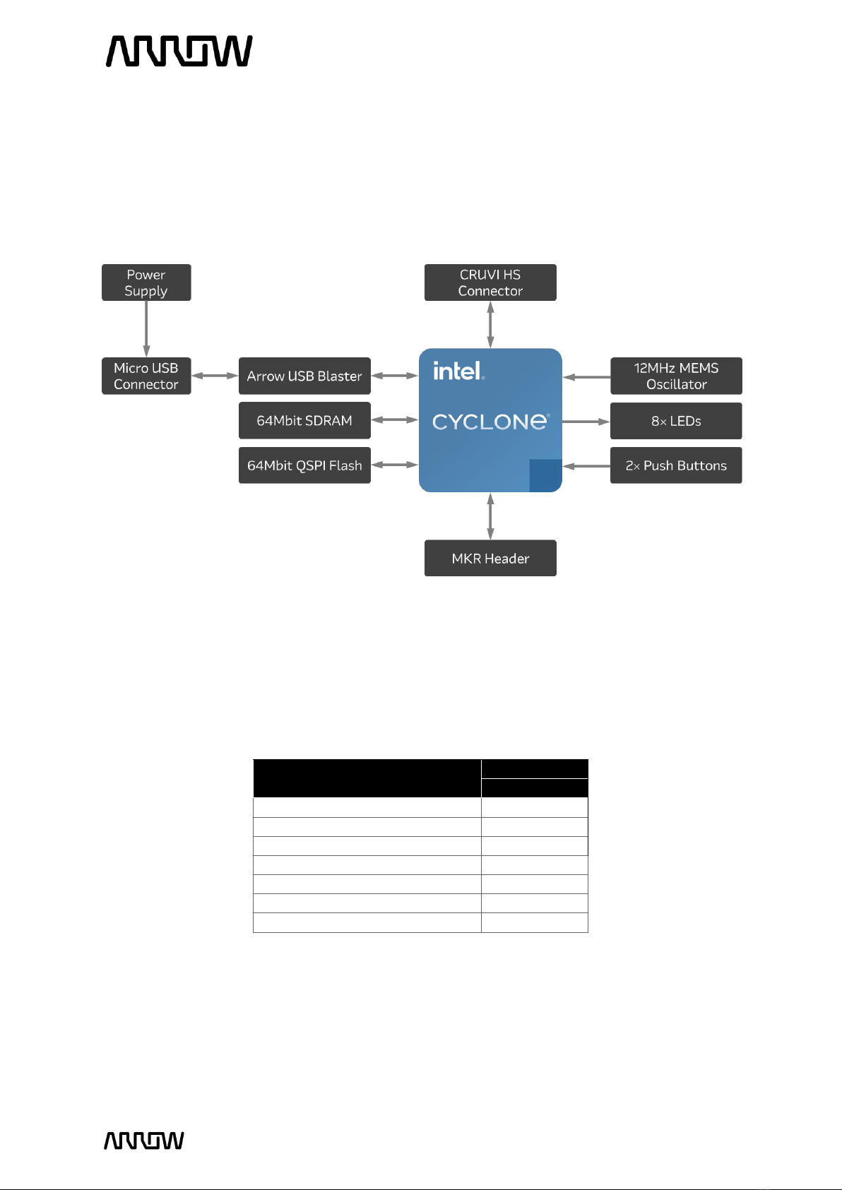
2.2 Block Diagram.........................................................................................................................................................8
Connections and Peripherals of the CYC5000 Board ................................................. 10
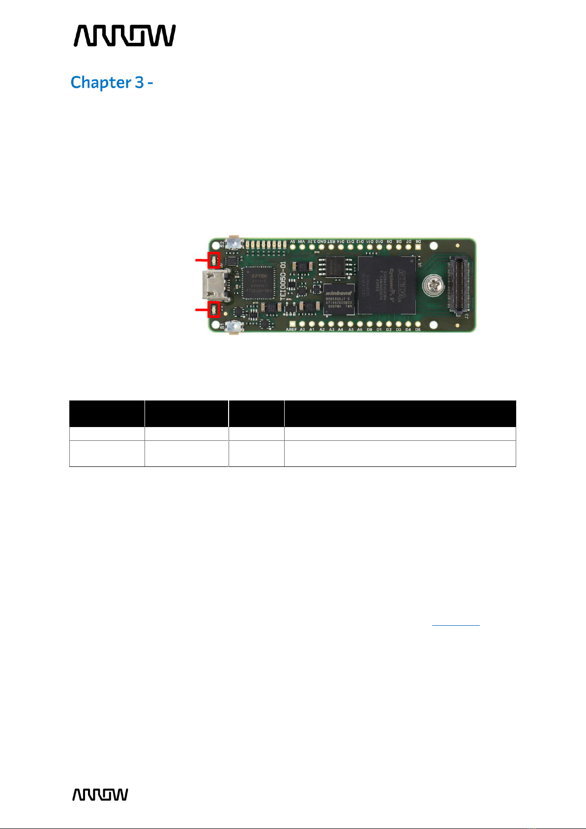
3.1 Board Status Elements.....................................................................................................................................10
3.2 Clock Circuitry ......................................................................................................................................................10
3.3 Peripherals Connected to the FPGA ..........................................................................................................11
3.3.1 Communication and Configuration...................................................................................................11
3.3.2 QSPI Configuration Flash Memory ...................................................................................................13
3.3.3 SDRAM Memory.........................................................................................................................................14
3.3.4 CRUVI HS Connector ...............................................................................................................................16
3.3.5 Arduino Header ..........................................................................................................................................18
3.3.6 LEDs .................................................................................................................................................................19
3.3.7 Push Buttons ..............................................................................................................................................20
3.3.8 Power Tree....................................................................................................................................................21
Software and Driver Installation..................................................................................... 23
4.1 Installing Quartus Prime Software............................................................................................................23
4.2 Installing Arrow USB Programmer2..........................................................................................................25
4.3 License ..................................................................................................................................................................... 27
New Project with CYC5000 ..............................................................................................29
5.1 Creating a new Blinky Project with CYC5000 .....................................................................................29
5.2 Building a Blinky Project with CYC5000................................................................................................33
5.2.1 Block Diagram............................................................................................................................................33
5.2.2 Components of the Design .................................................................................................................34
5.2.3 Catalog IP .....................................................................................................................................................34
5.2.4 Create and Configure PLL ....................................................................................................................34
5.2.5 Create and Configure the Counter..................................................................................................36
5.2.6 Create and Configure the Multiplexer...........................................................................................39
5.2.7 Adding the Components to the Schematic..................................................................................41
5.2.8 Connecting the Components .............................................................................................................43

CYC5000 User Guide www.arrow.com
Page | 3 March 2023
5.2.9 Add inputs, outputs to the schematic ...........................................................................................46
5.2.10 Analysis and Synthesis ..........................................................................................................................49
5.2.11 Adding Timing Constraints..................................................................................................................49
5.2.12 Pinning Assignments ...............................................................................................................................51
5.2.13 Compiling the Design .............................................................................................................................54
5.2.14 Reading the Compilation Report......................................................................................................55
Configuring the CYC5000................................................................................................. 57
6.1 Configure the FPGA in JTAG mode ........................................................................................................... 57
6.2 QSPI flash memory programming...............................................................................................................61
6.2.1 Programming File generation .............................................................................................................61
6.2.2 Device Programming ..............................................................................................................................64
6.3 Testing the Design .............................................................................................................................................66
Common Issues and Fixes.................................................................................................. 67
Appendix ..............................................................................................................................68
8.1 Revision History ..................................................................................................................................................68
8.2 Legal Disclaimer..................................................................................................................................................69

CYC5000 User Guide www.arrow.com
Page | 4 March 2023
Table of Figures
Figure 1 –CYC5000 Board (top view) ..............................................................................................................................7
Figure 2 –CYC5000 Block Diagram.................................................................................................................................8
Figure 3 –Position of Indication LEDs...........................................................................................................................10
Figure 4 –CYC5000 Clock Tree ........................................................................................................................................11
Figure 5 –FTDI Connections ..............................................................................................................................................12
Figure 6 –JTAG Connections.............................................................................................................................................13
Figure 7 –Configuration Flash Connections ..............................................................................................................14
Figure 8 –SDRAM Connections........................................................................................................................................14
Figure 9 –CRUVI HS Connections ...................................................................................................................................16
Figure 10 - Arduino Header Connections.....................................................................................................................18
Figure 11 –LED Connections..............................................................................................................................................20
Figure 12 –Button Connections........................................................................................................................................21
Figure 13 –Power Tree Connections ............................................................................................................................. 22

CYC5000 User Guide www.arrow.com
Page | 5 March 2023
CYC5000 IoT / Maker Board
1.1 About Arrow CYC5000 Board
The CYC5000 is a customizable IoT / Maker Board ready for evaluation, development, and/or use
in a product. The board is based on Cyclone V FPGA, which is optimized to simultaneously
accommodate the shrinking power consumption, cost, and time-to-market requirements,
furthermore, increasing bandwidth requirements for a wide spectrum of general logic and DSP
applications. The ready-to-use hard intellectual property (IP) blocks in the core FPGA fabric, such
as variable precision digital signal processing (DSP) blocks, and multiport memory controllers
consume less power and free up more logic resources, which provides sufficient resources to
implement other functions such as Nios II 32-bit microcontroller IP or various interface controls.
The CYC5000 is equipped with an Arrow USB Programmer2, SDRAM, flash memory, CRUVI HS
and ARDUINO MKR connectors making it a fully featured plug-and-play solution without any
additional costs.
The CYC5000 board contains all the tools needed to use the board in conjunction with a
computer that runs a 64-bit Linux / Microsoft Windows 10 operating system or later.
1.2 Useful Links
A set of useful links that can be used to get relevant information about the CYC5000 board or
the Cyclone V FPGA.
•CYC5000 at Arrow Shop
•CYC5000 at Trenz Electronic Shop
•Intel Cyclone V Webpage
•CYC5000 Wiki Page

CYC5000 User Guide www.arrow.com
Page | 7 March 2023
Introduction to the CYC5000 Board
2.1 Layout and Components
Figure 1 shows the top view of the board. It depicts the layout of the board and indicates the
location of the various connectors and key components.
The following features are available on the CYC5000 board:
•Intel Cyclone V 5CEBA2U15C8N device
•Arrow USB Programmer2 on-board for programming; JTAG Mode
•64Mbit SDRAM up to 166MHz
•64Mbit QSPI Configuration flash memory
•CRUVI HS Connector
•USB-to-JTAG
•GPIO-FTDI
•Arduino MKR Header
•12MHz MEMS Oscillator
•8red user LEDs
•2board indicaton LEDs
•2user push buttons
Figure 1 –CYC5000 Board (top view)

CYC5000 User Guide www.arrow.com
Page | 8 March 2023
2.2 Block Diagram
Figure 2 represents the block diagram of the board. All the connections are established through
the Cyclone V FPGA device to provide maximum flexibility for users. Users can configure the
FPGA to implement any system design.
FPGA Device
•Intel Cyclone V 5CEBA2U15C8N device.
Features of the FPGA on the CYC5000 Board:
Resources
Device
5CEBA2
Logic Elements (kLE)
25
Adaptive Logic Module (ALM)
9,430
M10K Memory (Kb)
1,760
Variable-precision DSP Block
25
18 18 Multiplier
50
PLLs
4
I/O
176
Memory Devices
•64Mbit external SDRAM memory
•64Mbit external QSPI Flash memory
Figure 2 –CYC5000 Block Diagram

CYC5000 User Guide www.arrow.com
Page | 9 March 2023
Configuration and Debug
•On-board Arrow USB Programmer2 (micro-USB type B connector) –JTAG mode
Connectors & Headers
•CRUVI HS Connector
•Arduino MKR compatible Header
Buttons and Indicators
•2Side-Buttons
•8red user LEDs
•2board status LEDs
Power
•Recommended external supply voltage range: +5.0 V (nominal)
•Recommended I/O signal voltage range: 0 to +3.3 V

CYC5000 User Guide www.arrow.com
Page | 10 March 2023
Connections and Peripherals of the CYC5000
Board
3.1 Board Status Elements
In addition to the 8 user LEDs that the FPGA can control, there are 2 additional board-specific
status LEDs that can indicate the status of the board.
Board
Reference
LED Name
Colour
Description
D1
3.3V
Green
On when 3.3V power is active
D10
CONF_DONE
Red
Off when configuration data was loaded to
Cyclone V device without error
3.2 Clock Circuitry
The external clock of the system can be seen in Figure 4. The default clock (CLK12M) is at 12MHz
and is connected and driving the FPGA’s user logic and the Arrow USB Programmer2. There is an
optional clock input from CRUVI HS Connector, where you can add another preferred clock
source to the FPGA (REFCLK). Both clock signals drive the internal PLLs of the FPGA.
For more information on clocks and PLLs of the Cyclone V, please refer to this document.
Figure 3 –Position of Indication LEDs

CYC5000 User Guide www.arrow.com
Page | 11 March 2023
Board
Reference
FPGA Pin No.
Pin Func.
Description
I/O Std
CLK12M
PIN_F14
Input
12MHz clock input
3.3 V
REFCLK
PIN_G14
Input
Optional clock input
3.3 V
3.3 Peripherals Connected to the FPGA
3.3.1 Communication and Configuration
The CYC5000 board uses a single chip to perform configuration of the device and communication
over USB.
3.3.1.1 USB Communication
The FTDI chip converts signals from USB 2.0 to a variety of standard serial and parallel interfaces.
Channel A of FTDI chip is used in MPPSE mode for JTAG. Channel B is routed to FPGA and is
usable for other standard interfaces.
Figure 4 –CYC5000 Clock Tree

CYC5000 User Guide www.arrow.com
Page | 12 March 2023
Board
Reference
FPGA Pin No.
Pin Func.
Description
I/O Std
BDBUS0
PIN_E18
Bidir
D[0] of bidirectional data bus
3.3 V
BDBUS1
PIN_F16
Bidir
D[1] of bidirectional data bus
3.3 V
BDBUS2
PIN_H17
Bidir
D[2] of bidirectional data bus
3.3 V
BDBUS3
PIN_H16
Bidir
D[3] of bidirectional data bus
3.3 V
BDBUS4
PIN_J16
Bidir
D[4] of bidirectional data bus
3.3 V
BDBUS5
PIN_G15
Bidir
D[5] of bidirectional data bus
3.3 V
BDBUS6
PIN_J14
Bidir
D[6] of bidirectional data bus
3.3 V
BDBUS7
PIN_L15
Bidir
D[7] of bidirectional data bus
3.3 V
BCBUS0
PIN_G13
Bidir
D[0] of bidirectional data bus
3.3 V
BCBUS1
PIN_H13
Bidir
D[1] of bidirectional data bus
3.3 V
BCBUS2
PIN_J15
Bidir
D[2] of bidirectional data bus
3.3 V
BCBUS3
PIN_J13
Bidir
D[3] of bidirectional data bus
3.3 V
BCBUS4
PIN_K16
Bidir
D[4] of bidirectional data bus
3.3 V
BCBUS5
PIN_K18
Bidir
D[5] of bidirectional data bus
3.3 V
BCBUS6
PIN_K17
Bidir
D[6] of bidirectional data bus
3.3 V
BCBUS7
PIN_L16
Bidir
D[7] of bidirectional data bus
3.3 V
Figure 5 –FTDI Connections

CYC5000 User Guide www.arrow.com
Page | 13 March 2023
3.3.1.2 JTAG Chain Configuration
There are two types of configuration methods supported by CYC5000:
1. JTAG Configuration: configuration using JTAG ports. JTAG configuration scheme allows you
to directly configure the device core through JTAG pins (TDI, TDO, TMS and TCK pins). The
Quartus Prime software automatically generates a .sof that can be downloaded to the
Cyclone V with a download cable through the Quartus Prime Programmer. This function is
only available via the On-board Arrow USB Programmer2.
2. Configuration from QSPI flash: configuration using external flash. Before configuration, you
need to program the configuration data .jic into the configuration flash memory which
provides non-volatile storage for the bit stream. The information is retained within flash
memory even if the CYC5000 is turned off. When the board is powered on, the configuration
data in the flash memory is automatically loaded into the Cyclone V FPGA.
Board
Reference
FPGA Pin No.
Pin Func.
Description
I/O Std
TCK
PIN_L6
Input
Test Interface Clock
3.3 V
TDI
PIN_N6
Input
Test Data In
3.3 V
TDO
PIN_P5
Output
Test Data Out
3.3 V
TMS
PIN_P6
Input
Test Mode Select
3.3 V
For detailed information about how to configure the Cyclone V, please refer to Chapter 6.
3.3.2 QSPI Configuration Flash Memory
The CYC5000 board is integrated with a 64MBit of QSPI flash memory that can be used for user
data and programming non-volatile storage. The configuration bitstream is downloaded into the
configuration device which automatically loads the configuration data into the Cyclone V when
the board is powered on. Device memory capacity not consumed storing configuration data can
be used as general-purpose non-volatile memory, which with its operation of up to 133MHz is
perfect for program and data storage. Several interfaces available with Nios II embedded
Figure 6 –JTAG Connections

CYC5000 User Guide www.arrow.com
Page | 14 March 2023
processors allow you to access the serial configuration device as a memory module connected
to your embedded system.
Board
Reference
FPGA Pin No.
Pin Func.
Description
I/O Std
AS_NCS
PIN_P3
Output
Chip Select
3.3 V
AS_DCLK
PIN_K6
Output
Clock
3.3 V
AS_DATA0
PIN_V1
Bidir
Data [0]
3.3 V
AS_DATA1
PIN_U2
Bidir
Data [1]
3.3 V
AS_DATA2
PIN_U3
Bidir
Data [2]
3.3 V
AS_DATA3
PIN_M5
Bidir
Data [3]
3.3 V
3.3.3 SDRAM Memory
The CYC5000 board supports single-chip SDRAM with 64Mbit density which can operate up to
166 MHz clock frequency. Below are the connections and pinning of the SDRAM used in the
CYC5000.
Figure 7 –Configuration Flash Connections
Figure 8 –SDRAM Connections

CYC5000 User Guide www.arrow.com
Page | 15 March 2023
Board
Reference
FPGA Pin No.
Pin Func.
Description
I/O Std
A0
PIN_R13
Output
SDRAM Address [0]
3.3 V
A1
PIN_U12
Output
SDRAM Address [1]
3.3 V
A2
PIN_V12
Output
SDRAM Address [2]
3.3 V
A3
PIN_V13
Output
SDRAM Address [3]
3.3 V
A4
PIN_V15
Output
SDRAM Address [4]
3.3 V
A5
PIN_V16
Output
SDRAM Address [5]
3.3 V
A6
PIN_T16
Output
SDRAM Address [6]
3.3 V
A7
PIN_U15
Output
SDRAM Address [7]
3.3 V
A8
PIN_P14
Output
SDRAM Address [8]
3.3 V
A9
PIN_T15
Output
SDRAM Address [9]
3.3 V
A10
PIN_M13
Output
SDRAM Address [10]
3.3 V
A11
PIN_P15
Output
SDRAM Address [11]
3.3 V
A12
PIN_N16
Output
SDRAM Address [12]
3.3 V
A13
PIN_R16
Output
SDRAM Address [13]
3.3 V
BA0
PIN_T12
Output
SDRAM Bank Address [0]
3.3 V
BA1
PIN_N13
Output
SDRAM Bank Address [1]
3.3 V
RAS
PIN_P13
Output
SDRAM Row Address Strobe
3.3 V
CAS
PIN_M14
Output
SDRAM Column Address Strobe
3.3 V
WE
PIN_N12
Output
SDRAM Write Enable
3.3 V
CS
PIN_L13
Output
SDRAM Chip Select
3.3 V
CLK
PIN_P16
Output
SDRAM Input Clock
3.3 V
CKE
PIN_T14
Output
SDRAM Clock Enable
3.3 V
DQ0
PIN_U4
Bidir
SDRAM Data [0]
3.3 V
DQ1
PIN_T4
Bidir
SDRAM Data [1]
3.3 V
DQ2
PIN_V6
Bidir
SDRAM Data [2]
3.3 V
DQ3
PIN_U5
Bidir
SDRAM Data [3]
3.3 V
DQ4
PIN_V7
Bidir
SDRAM Data [4]
3.3 V
DQ5
PIN_T5
Bidir
SDRAM Data [5]
3.3 V
DQ6
PIN_V8
Bidir
SDRAM Data [6]
3.3 V
DQ7
PIN_U8
Bidir
SDRAM Data [7]
3.3 V
DQ8
PIN_P10
Bidir
SDRAM Data [8]
3.3 V
DQ9
PIN_P9
Bidir
SDRAM Data [9]
3.3 V
DQ10
PIN_T11
Bidir
SDRAM Data [10]
3.3 V
DQ11
PIN_R9
Bidir
SDRAM Data [11]
3.3 V
DQ12
PIN_R11
Bidir
SDRAM Data [12]
3.3 V
DQ13
PIN_T9
Bidir
SDRAM Data [13]
3.3 V
DQ14
PIN_V10
Bidir
SDRAM Data [14]
3.3 V
DQ15
PIN_U9
Bidir
SDRAM Data [15]
3.3 V
DQM0
PIN_U13
Output
SDRAM Lower Data Mask
3.3 V
DQM1
PIN_U14
Output
SDRAM Upper Data Mask
3.3 V

CYC5000 User Guide www.arrow.com
Page | 16 March 2023
3.3.4 CRUVI HS Connector
The CYC5000 board has one CRUVI HS connector. CRUVI HS is an open ecosystem which makes
it possible to add a big variety of interfaces to the system, that can require high-speed signalling
as well as low-speed device interface support.
The voltage level of High-Speed interfaces can be selected between 1.8V and 3.3V which ensures
that these I/Os are compatible with the high-speed LVDS standard as well as the lower-speed
GPIOs.
The CYC5000 board provides +5V and +3.3V power to the mezzanine card through the CRUVI HS
connector.
For custom add-on cards with CRUVI HS interface, the recommended counterpart is
ST4-30-1.50-L-D from Samtec.
Below is the connection diagram and pinning information.
Board
Reference
FPGA Pin
No.
CRUVI HS
No.
Pin
Func.
Description
I/O Std
A0_P
PIN_A12
14
Output
High-Speed Differential
Transmitter A[0]_p
1.8 V /
3.3 V
A0_N
PIN_B12
16
Output
High-Speed Differential
Transmitter A[0]_n
1.8 V /
3.3 V
A1_P
PIN_A11
20
Output
High-Speed Differential
Transmitter A[1]_p
1.8 V /
3.3 V
A1_N
PIN_A10
22
Output
High-Speed Differential
Transmitter A[1]_n
1.8 V /
3.3 V
A2_P
PIN_A14
26
Output
High-Speed Differential
Transmitter A[2]_p
1.8 V /
3.3 V
Figure 9 –CRUVI HS Connections

CYC5000 User Guide www.arrow.com
Page | 17 March 2023
Board
Reference
FPGA Pin
No.
CRUVI HS
No
Pin
Func.
Description
I/O Std
A2_N
PIN_A15
28
Output
High-Speed Differential
Transmitter A[2]_n
1.8 V /
3.3 V
A3_P
PIN_A16
32
Output
High-Speed Differential
Transmitter A[3]_p
1.8 V /
3.3 V
A3_N
PIN_A17
34
Output
High-Speed Differential
Transmitter A[3]_n
1.8 V /
3.3 V
A4_P
PIN_F9
38
Input
High-Speed Differential Receiver
A[4]_p
1.8 V /
3.3 V
A4_N
PIN_F10
40
Input
High-Speed Differential Receiver
A[4]_n
1.8 V /
3.3 V
A5_P
PIN_B7
44
Input
High-Speed Differential Receiver
A[5]_p
1.8 V /
3.3 V
A5_N
PIN_B8
46
Input
High-Speed Differential Receiver
A[5]_n
1.8 V /
3.3 V
B0_P
PIN_B17
15
Output
High-Speed Differential
Transmitter B[0]_p
1.8 V /
3.3 V
B0_N
PIN_B18
17
Output
High-Speed Differential
Transmitter B[0]_n
1.8 V /
3.3 V
B1_P
PIN_A7
21
Output
High-Speed Differential
Transmitter B[1]_p
1.8 V /
3.3 V
B1_N
PIN_A6
23
Output
High-Speed Differential
Transmitter B[1]_n
1.8 V /
3.3 V
B2_P
PIN_C13
37
Input
High-Speed Differential Receiver
B[2]_p
1.8 V /
3.3 V
B2_N
PIN_C12
29
Input
High-Speed Differential Receiver
B[2]_n
1.8 V /
3.3 V
B3_P
PIN_E8
33
Input
High-Speed Differential Receiver
B[3]_p
1.8 V /
3.3 V
B3_N
PIN_F7
35
Input
High-Speed Differential Receiver
B[3]_n
1.8 V /
3.3 V
B4_P
PIN_G6
39
Input
High-Speed Differential Receiver
B[4]_p
1.8 V /
3.3 V
B4_N
PIN_F6
41
Input
High-Speed Differential Receiver
B[4]_n
1.8 V /
3.3 V
B5_P
PIN_B4
45
Input
High-Speed Differential Receiver
B[5]_p
1.8 V /
3.3 V
B5_N
PIN_B5
47
Input
High-Speed Differential Receiver
B[5]_n
1.8 V /
3.3 V
HSI
PIN_D16
10
Bidir
Serial In or High-Speed Differential
Transmitter A[6]_p
1.8 V /
3.3 V
HSMIO
PIN_C16
2
Bidir
Serial Data I/O or High-Speed
Differential Transmitter A[6]_n
1.8 V /
3.3 V
HSO
PIN_B14
6
Output
Serial Out or High-Speed
Differential Transmitter A[7]_p
1.8 V /
3.3 V
HSRST
PIN_B15
8
Output
Serial Reset or High-Speed
Differential Transmitter A[7]_n
1.8 V /
3.3 V
SMB_ALERT
PIN_G17
3
Input
SMBus interrupt signal
3.3 V
SMB_SDA
PIN_H18
5
Bidir
SMBus Data Line
3.3 V
SMB_SCL
PIN_F17
7
Output
SMBus Data Clock Line
3.3 V

CYC5000 User Guide www.arrow.com
Page | 18 March 2023
Board
Reference
FPGA Pin
No.
CRUVI HS
No
Pin
Func.
Description
I/O Std
SDI
PIN_F4
51
Input
Master Input Slave Output
3.3 V
SDO
PIN_J3
53
Output
Master Output Slave Input
3.3 V
SEL
PIN_E3
55
Output
Chip Select
3.3 V
MODE
PIN_J4
57
Bidir
Mode pin, User IO
3.3 V
SCK
PIN_E2
59
Output
Clock
3.3 V
REFCLK
PIN_G14
11
Input
Clock Input
3.3 V
5V
-
60
PWR
5V power to the connector
-
3.3V
-
4, 9
PWR
3.3V power to the connector
-
ADJ
-
36
PWR
HS IO Bank voltage
-
GND
-
12, 13, 18,
19, 24, 25,
30, 31, 36,
37, 42, 43,
48, 49, 54
PWR
Ground to the connector
-
n.c.
-
1, 50, 52,
56, 58
-
Not connected
-
VSEL
PIN_N10
-
Output
HS IO Bank voltage select:
- VSEL = ‘0’; ADJ = 1.8V
- VSEL = ‘1’; ADJ = 3.3V
3.3 V
3.3.5 Arduino Header
The CYC5000 board offers connectivity to classic Arduino MKR compatible shields that could
also alternatively be used as GPIOs. The MKR connectors offer up to 23 digital I/Os.
Figure 10 - Arduino Header Connections

CYC5000 User Guide www.arrow.com
Page | 19 March 2023
Board
Reference
FPGA Pin
No.
Arduino
Header
Pin
Func.
Description
I/O Std
AREF
PIN_V17
J1 / 1
Bidir
Input reference voltage or GPIO
3.3 V
AIN0
PIN_U17
J1 / 2
Bidir
GPIO [0]
3.3 V
AIN1
PIN_T17
J1 / 3
Bidir
GPIO [1]
3.3 V
AIN2
PIN_U18
J1 / 4
Bidir
GPIO [2]
3.3 V
AIN3
PIN_R17
J1 / 5
Bidir
GPIO [3]
3.3 V
AIN4
PIN_R18
J1 / 6
Bidir
GPIO [4]
3.3 V
AIN5
PIN_P18
J1 / 7
Bidir
GPIO [5]
3.3 V
AIN6
PIN_N17
J1 / 8
Bidir
GPIO [6]
3.3 V
D0
PIN_N18
J1 / 9
Bidir
Digital I/O [0]
3.3 V
D1
PIN_M18
J1 / 10
Bidir
Digital I/O [1]
3.3 V
D2
PIN_J18
J1 / 11
Bidir
Digital I/O [2]
3.3 V
D3
PIN_G18
J1 / 12
Bidir
Digital I/O [3]
3.3 V
D4
PIN_D18
J1 / 13
Bidir
Digital I/O [4]
3.3 V
D5
PIN_C18
J1 / 14
Bidir
Digital I/O [5]
3.3 V
D6
PIN_D1
J2 / 1
Bidir
Digital I/O [6]
3.3 V
D7
PIN_E1
J2 / 2
Bidir
Digital I/O [7]
3.3 V
D8
PIN_F1
J2 / 3
Bidir
Digital I/O [8]
3.3 V
D9
PIN_J1
J2 / 4
Bidir
Digital I/O [9]
3.3 V
D10
PIN_L2
J2 / 5
Bidir
Digital I/O [10]
3.3 V
D11
PIN_N2
J2 / 6
Bidir
Digital I/O [11]*
3.3V
D12
PIN_R1
J2 / 7
Bidir
Digital I/O [12]*
3.3 V
D13
PIN_R2
J2 / 8
Bidir
Digital I/O [13]
3.3 V
D14
PIN_T1
J2 / 9
Bidir
Digital I/O [14]
3.3 V
D11_R
PIN_M2
J2 / 6
Bidir
Digital I/O [11] with resistor*
3.3 V
D12_R
PIN_P1
J2 / 7
Bidir
Digital I/O [12] with resistor*
3.3 V
Reset
PIN_H4
J2 / 10
Bidir
System reset of the board,
controlled by the S1 user button
3.3 V
GND
-
J2 / 11
PWR
Ground of the connector
-
3.3V
-
J2 / 12
PWR
3.3V power to the connector
-
VIN
-
J2 / 13
PWR
User power into to the
CYC5000 Board
-
5V
-
J2 / 14
PWR
5V power to the connector
-
*Can only choose one, hence same name pinning
3.3.6 LEDs
There are eight red user-controllable LEDs connected to the FPGA. Each LED is driven directly
and individually by the Cyclone V FPGA, driving its associated pin to a high logic level for on or
low logic level for off.

CYC5000 User Guide www.arrow.com
Page | 20 March 2023
Board
Reference
FPGA Pin No.
Pin Func.
I/O Std
LED1
PIN_P4
Output
3.3 V
LED2
PIN_M4
Output
3.3 V
LED3
PIN_M3
Output
3.3 V
LED4
PIN_N3
Output
3.3 V
LED5
PIN_V2
Output
3.3 V
LED6
PIN_T2
Output
3.3 V
LED7
PIN_L1
Output
3.3 V
LED8
PIN_K1
Output
3.3 V
3.3.7 Push Buttons
The board has two push buttons connected to the FPGA. Push buttons drive their associated pins
low logic level when pressed and high logic level when released.
Figure 11 –LED Connections
Table of contents
Other Arrow Motherboard manuals

Arrow
Arrow einfochips eragon 660 User manual

Arrow
Arrow BeMicro CV A9 Operating and maintenance manual

Arrow
Arrow MAX1000 User manual

Arrow
Arrow CYC1000 User manual

Arrow
Arrow verical LINEAR TECHNOLOGY DC1762A-A Quick setup guide

Arrow
Arrow SD 600eval Instructions for use

Arrow
Arrow verical RENESAS YSTREAM-IT-RZ-V2 User manual

Arrow
Arrow DC333A User manual

Arrow
Arrow verical CYPRESS S6SBP201A1AVA1001 User manual

Arrow
Arrow Everest-CortexM1-SFP+Loop-Demo User manual